Äîêóìåíòàöèÿ è îïèñàíèÿ www.docs.chipfind.ru

ICSI reserves the right to make changes to its products at any time without notice in order to improve design and supply the best possible product. We assume no responsibility for any errors
which may appear in this publication. © Copyright 2000, Integrated Circuit Solution Inc.
FEATURES
Single 3.3V (± 0.3V) power supply
High speed clock cycle time -7: 133MHz<3-3-3>,
-8: 100MHz<2-2-2>
Fully synchronous operation referenced to clock
rising edge
Possible to assert random column access in
every cycle
Quad internal banks contorlled by A12 & A13
(Bank Select)
Byte control by LDQM and UDQM for
IS42S16400
Programmable Wrap sequence (Sequential /
Interleave)
Programmable burst length (1, 2, 4, 8 and full
page)
Programmable /CAS latency (2 and 3)
Automatic precharge and controlled precharge
CBR (Auto) refresh and self refresh
X8, X16 organization
LVTTL compatible inputs and outputs
4,096 refresh cycles / 64ms
Burst termination by Burst stop and Precharge
command
Package 400mil 54-pin TSOP-2
DESCRIPTION
The IS42S8800 and IS42S16400 are high-speed 67,
108,864-bit synchronous dynamic random-access
moeories, organized as 2,097,152 x 8 x 4 and 1,048,
576 x 16 x 4 (word x bit x bank), respectively.
The synchronous DRAMs achieved high-speed data
transfer using the pipeline architecture and clock
frequency up to 133MHz for -7. All input and outputs
are synchronized with the postive edge of the clock.
The synchronous DRAMs are compatible with Low
Voltage TTL (LVTTL).These products are pack-aged
in 54-pin TSOP-2.
IS42S8800/IS42S8800L
IS42S16400/IS42S16400L
2(1)M Words x 8(16) Bits x 4 Banks (64-MBIT)
SYNCHRONOUS DYNAMIC RAM
Integrated Circuit Solution Inc.
1
DR007-0A
IS42S8800/IS42S8800L
IS42S16400/IS42S16400L
2
Integrated Circuit Solution Inc.
DR007-0A
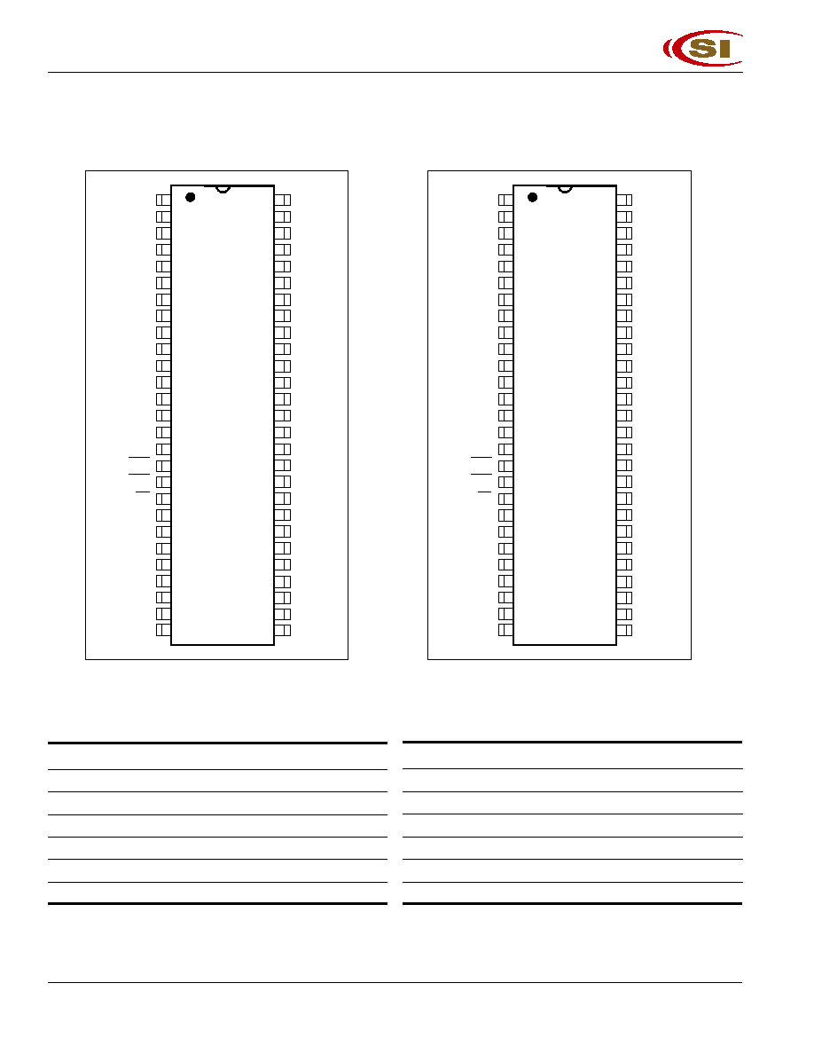
PIN CONFIGURATIONS
54-Pin TSOP-2 (IS42S8800)
DQM
DQ Mask Enable
A0-11
Address Input
BA0,1
Bank Address
V
DD
Power Supply
V
DDQ
Power Supply for DQ
V
SS
Ground
V
SSQ
Ground for DQ
PIN DESCRIPTIONS
CLK
Master Clock
CKE
Clock Enable
CS
Chip Select
RAS
Row Address Strobe
CAS
Column Address Strobe
WE
Write Enable
DQ0 ~ DQ15
Data I/O
54-Pin TSOP-2 (IS42S16400)
1
2
3
4
5
6
7
8
9
10
11
12
13
14
15
16
17
18
19
20
21
22
23
24
25
26
27
54
53
52
51
50
49
48
47
46
45
44
43
42
41
40
39
38
37
36
35
34
33
32
31
30
29
28
VDD
DQ0
VDDQ
NC
DQ1
VSSQ
NC
DQ2
VDDQ
NC
DQ3
VSSQ
NC
VDD
NC
WE
CAS
RAS
CS
BA0
BA1
A10
A0
A1
A2
A3
VDD
VSS
DQ7
VSSQ
NC
DQ6
VDDQ
NC
DQ5
VSSQ
NC
DQ4
VDDQ
NC
VSS
NC
DQM
CLK
CKE
NC
A11
A9
A8
A7
A6
A5
A4
VSS
1
2
3
4
5
6
7
8
9
10
11
12
13
14
15
16
17
18
19
20
21
22
23
24
25
26
27
54
53
52
51
50
49
48
47
46
45
44
43
42
41
40
39
38
37
36
35
34
33
32
31
30
29
28
VDD
DQ0
VDDQ
DQ1
DQ2
VSSQ
DQ3
DQ4
VDDQ
DQ5
DQ6
VSSQ
DQ7
VDD
LDQM
WE
CAS
RAS
CS
BA0
BA1
A10
A0
A1
A2
A3
VDD
VSS
DQ15
VSSQ
DQ14
DQ13
VDDQ
DQ12
DQ11
VSSQ
DQ10
DQ9
VDDQ
DQ8
VSS
NC
DQM
CLK
CKE
NC
A11
A9
A8
A7
A6
A5
A4
VSS
IS42S8800/IS42S8800L
IS42S16400/IS42S16400L
Integrated Circuit Solution Inc.
3
DR007-0A
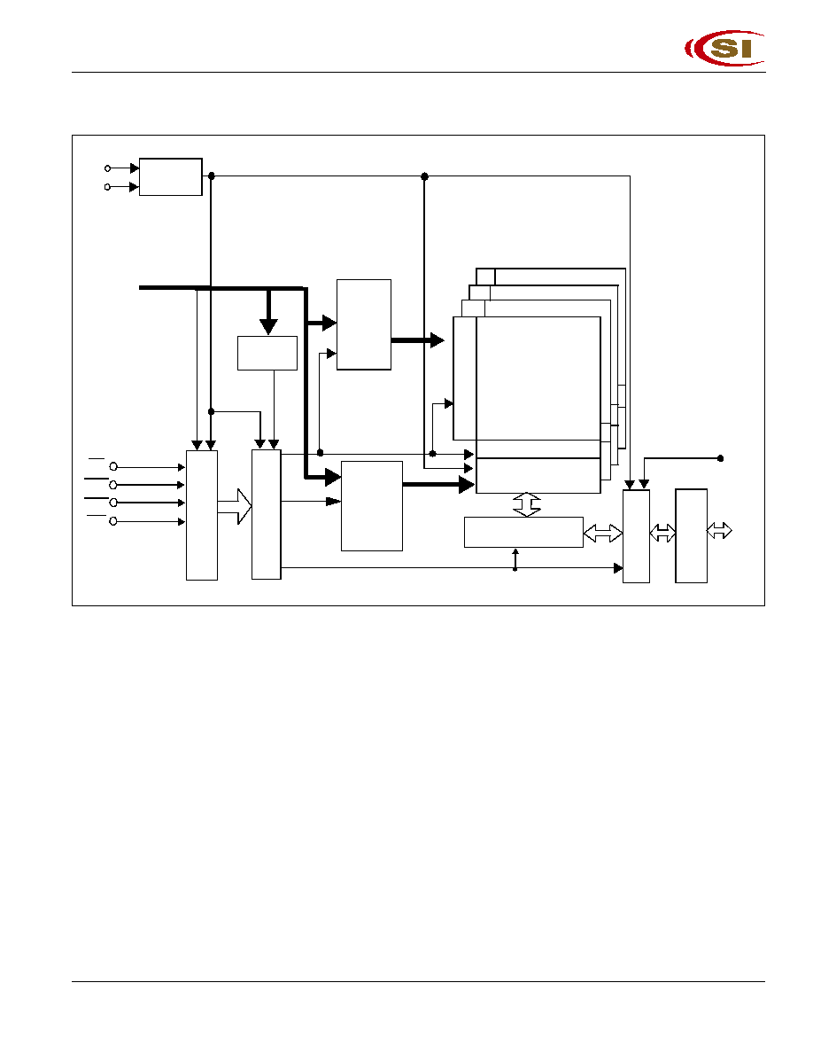
FUNCTIONAL BLOCK DIAGRAM
CLK
CKE
Clock
Generator
CS
RAS
Mode
Register
Column
Address
Buffer
&
Burst
Counter
CAS
WE
C
o
mm
and D
e
c
ode
r
C
ont
r
o
l
Lo
gic
Address
Row
Address
Buffer
&
Refresh
Counter
Bank B
Bank A
Sense Amplifier
Column Decoder &
Latch Circuit
R
o
w
D
e
c
oder
Data Control Circuit
DQ
DQM
La
tc
h
C
i
r
c
ui
t
In
put
&
O
u
t
p
ut
Bu
f
f
e
r
Bank C
Bank D
IS42S8800/IS42S8800L
IS42S16400/IS42S16400L
4
Integrated Circuit Solution Inc.
DR007-0A
PIN FUNCTIONS
Symbol
Type
Function (In Detail)
CLK
Input Pin
Maste Clock: Other inputs signals are referenecd to the CLK rising edge
CKE
Input Pin
Clock Enable: CKE HIGH activates, and CKE LOW deactivates internal
clock signals,device input buffers and output drivers. Deactivating the clock
provides PRECHARGE POWER-DOWN and SELF REFRESH operation
(all banks idle), or ACTIVE POWER-DOWN (row ACTIVE in any bank).
CS
Input Pin
Chip Select: +5 enables (registered LOW) and disables (registered HIGH)
the com-mand decoder. All commands are masked when +5 is registered
HIGH. +5 provides for external bank selection on systems with multiple
banks. +5 is considered part of the command code.
RAS, CAS, WE
Input Pin
Command Inputs:
RAS
,
CAS
and
WE
(along with +5) define the command
being entered.
A0-A11
Input Pin
Address Inputs: Provide the row address for ACTIVE commands, and the
column address and AUTO PRECHARGE bit for READ/WRITE
commands, to select one loca-tion out of the memory array in the respec-
tive bank. The row address is specified by A0-A11. The column address is
specified by A0-A8 (IS42S8800) / A0-A7 (IS42S16400)
BA0,BA1
Input Pin
Bank Address Inputs: BA0 and BA1 define to which bank an ACTIVE,
READ, WRITE or PRECHARGE command is being applied.
DQM, UDQM ,LDQM
Input Pin
Address Inputs: Provide the row address for ACTIVE commands (row
address A0-A10), and the column address and AUTO PRECHARGE bit for
READ/WRITE com-mands (column address A0-A7 with A10 defining
AUTO PRECHARGE), to select one location out of the memory array in the
respective bank.
DQ0 to DQ15
I/O Pin
I
Data Input / Output: Data bus.
V
DD
,
V
SS
Power Supply Pin
Power Supply for the memory array and peripheral circuitry.
V
DDQ
,
V
SSQ
Power Supply Pin
Power Supply are supplied to the output buffers only.
IS42S8800/IS42S8800L
IS42S16400/IS42S16400L
Integrated Circuit Solution Inc.
5
DR007-0A
ABSOLUTE MAXIMUM RATINGS
(1)
Symbol
Parameters
Rating
Unit
V
,,
Supply Voltage (with respect to V
SS
)
0.5 to +4.6
V
V
,,3
Supply Voltage for Output (with respect to V
SSQ
)
0.5 to +4.6
V
V
I
Input Voltage
(with respect to V
SS
)
0.5 to V
DD
+0.5
V
V
O
Output Voltage
(with respect to V
SSQ
)
1.0 to V
DDQ
+0.5
V
I
O
Short circuit output current
50
mA
P
D
Power Dissipation (
T
A
= 25 °C)
1
W
T
OPT
Operating Temperature
0 to +70
°C
T
STG
Storage Temperature
65 to +150
°C
Notes:
1. Exposing the device to stress above those listed in Absolute Maximum Ratings could cause permanent
damage. The device is not meant to be operated under conditions outside the limits described in the
operational section of this specification. Exposure to Absolute Maximum Rating conditions for extended
periods may affect device reliability.
DC RECOMMENDED OPERATING CONDITIONS
(
At T
A
= 0 to +70°C unless otherwise noted)
Symbol
Parameter
Min.
Typ.
Max.
Unit
V
DD
Supply Voltage
3.0
3.3
3.6
V
V
DDQ
Supply Voltage for DQ
0
0
0
V
V
SS
Ground
3.0
3.3
3.6
V
V
SSQ
Ground for DQ
0
0
0
V
V
IH
High Level Input Voltage (all Inputs)
2.0
V
DD
+ 0.3
V
V
IL
Low Level Input Voltage (all Inputs)
-0.3
+0.8
V
CAPACITANCE CHARACTERISTICS
(At T
A
= 0 ~ 70°C, V
DD
= V
DDQ
= 3.3 ± 0.3V, V
SS
= V
SSQ
= 0V , unless otherwise note@)
Symbol
Parameter
Min.
Max.
Unit
C
IN
Input Capacitance, address & control pin
2.5
3.8
pF
C
CLK
I
nput Capacitance, CLK pin
2.5
3.5
pF
CI/O
Data Input/Output Capacitance
4.0
6.5
pF