Äîêóìåíòàöèÿ è îïèñàíèÿ www.docs.chipfind.ru

HT9320 Series
22-Memory Tone/Pulse Dialer
1
July 21, 1999
Features
·
Universal specification
·
Operating voltag0e: 2.0V~5.5V
·
Low standby current
·
Lowmemoryretentioncurrent:0.1mA(typ.)
·
Tone/pulse switchable
·
Interface with LCD driver
·
32 digits for redialing
·
32 digits for the SA memory dialing
·
One-key redialing
·
Pause and P®T key for PBX
·
3.58MHz crystal or ceramic resonator
·
Hand-free control
·
Hold-line control
·
Pause, P®T can be saved for redialing
·
On-hook store function
·
Keytone function
·
Lock function
·
Resistor options
-
M/B ratio
-
Flash function and flash time
-
Pause and P®T duration
-
Pulse number
-
Inter-digit pause time for 10pps
·
Memory number: 22 memories
General Description
The HT9320 series tone/pulse dialers are
CMOS LSI for telecommunication systems.
They are designed to meet various dialing spec-
ifications through resistor option matrix.
The HT9320 series are offered in six different
versions. The different functions of the six ver-
sions are listed in the selection table. The
HT9320A, HT9320H versions provide the
on-hook store function; the HT9320B version
provides the LCD interface function; the
HT9320K version provides the keytone func-
tion; the HT9320L version provides both the
LCD interface function and IDD lock function.
The six versions also supply the hold-line and
hand-free functions, which are suitable for feature
phone applications.
HT9320 series provide SA, Redial and 20
one-touch/two-touch memory dialing. If the
keyboard includes M1~M20 keys it can be used
as one-touch memory dialing. Otherwise, it
works as two-touch (PAGE®M1~M10) or
three-touch(A®PAGE®0~9) memory dialing
for speed dialing in either pulse or tone mode.
Patent Number: 64097, 86474, 113235(R.O.C.), 5424740(U.S.A.)
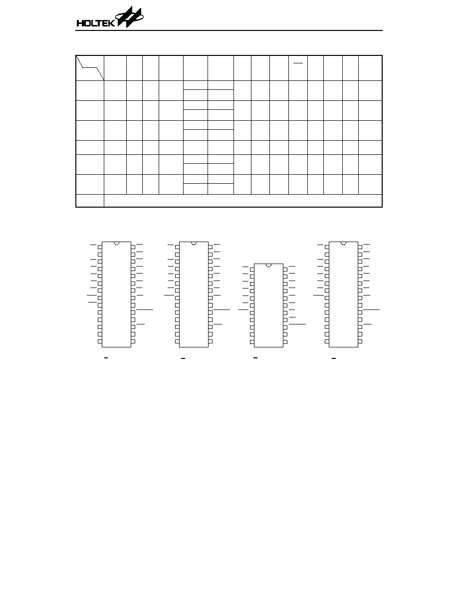
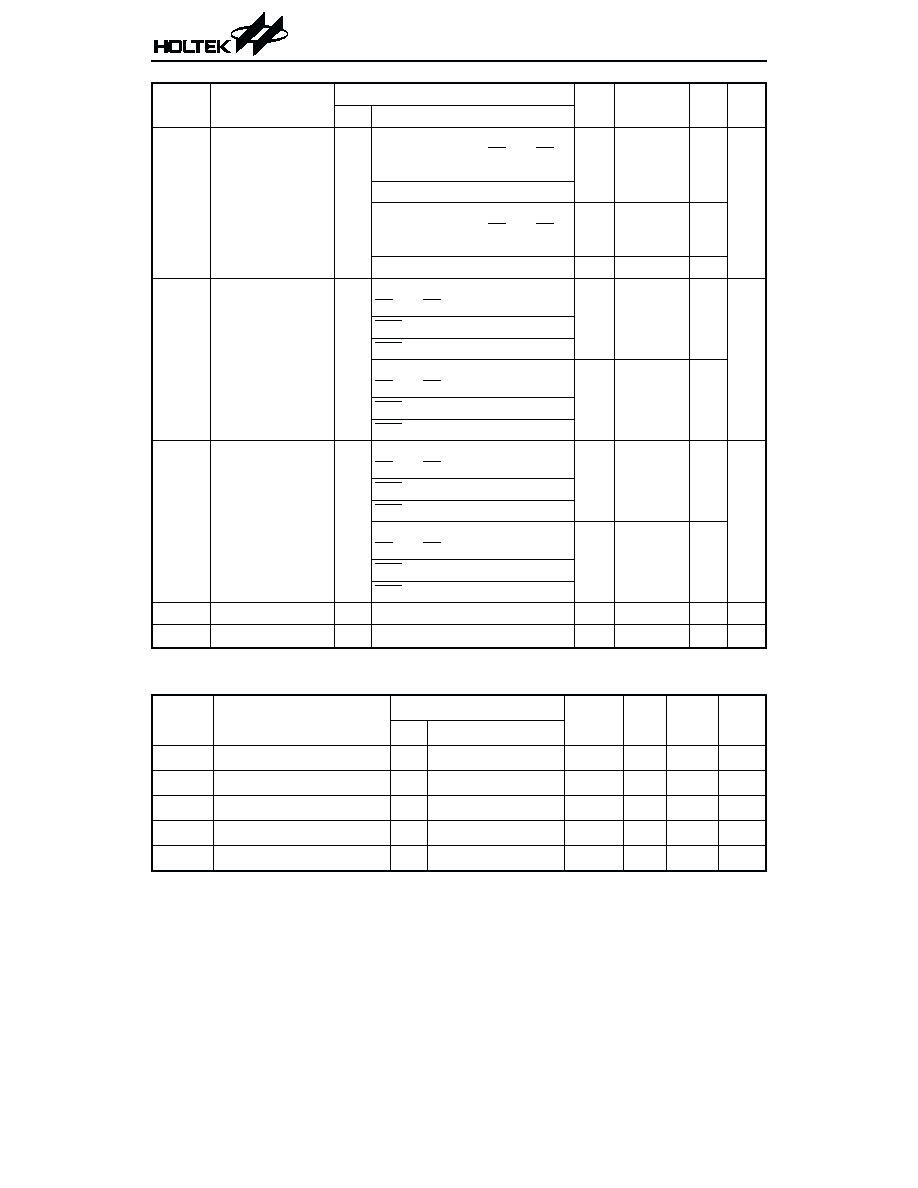
Selection Table
Function
Memory
Dialing
Hold-
Line
Hand-
Free
LCD
Interface
Flash
Function
Flash
Time
(ms)
Pulse
No.
Tone
Dura-
tion
(ms)
Inter-
Tone-
Pause
(ms)
M/B
Pin
IDD
Lock
Key-
Tone
Output
On-
Hook
Store
Package
Part No.
HT9320A
SA, R
M1~M20
Ö
Ö
¾
Control
600
N,
N+1
10-N
82.5
85.5
Ö
¾
¾
Ö
28 DIP
Digit
600/300/98
HT9320B
SA, R
M1~M20
Ö
Ö
Ö
Control
600
N,
N+1
10-N
82.5
85.5
¾
¾
¾
¾
28 DIP
Digit
600/300/98
HT9320C
SA, R
M1~M20
¾
¾
¾
Control
600
N,
N+1
10-N
82.5
85.5
¾
¾
¾
¾
22SKDIP
Digit
600/300/98
HT9320H
SA, R
M1~M20
Ö
Ö
¾
Digit
600/100
N
82.5
82.5
Ö
¾
¾
Ö
28 DIP
HT9320K
SA, R
M1~M20
Ö
Ö
¾
Control
600
N,
N+1
10-N
82.5
85.5
¾
¾
Ö
¾
28 DIP
Digit
600/300/98
HT9320L
SA, R
M1~M20
Ö
Ö
Ö
Control
600
N,
N+1
10-N
82.5
85.5
¾
Ö
¾
¾
28 DIP
Digit
600/300/98
HT9320L-X The same as HT9320L, but the voltage polarity of the row group and the column group are reversed.
Pin Assignment
HT9320
2
July 21, 1999
2 8
2 7
2 6
2 5
2 4
2 3
2 2
2 1
2 0
1 9
1 8
1 7
1 6
1 5
1
2
3
4
5
6
7
8
9
1 0
1 1
1 2
1 3
1 4
C 7
C 6
C 5
C 4
C 3
C 2
C 1
P O
H F O
X M U T E
D T M F
H D I
H D O
V S S
2 8
2 7
2 6
2 5
2 4
2 3
2 2
2 1
2 0
1 9
1 8
1 7
1 6
1 5
1
2
3
4
5
6
7
8
9
1 0
1 1
1 2
1 3
1 4
C 7
C 6
C 5
C 4
C 3
C 2
C 1
P O
H F O
X M U T E
D T M F
H D I
H D O
V S S
C 8
D O U T
R 1
R 2
R 3
R 4
R 5
H K S
C L O C K
H F I
M O D E
X 1
X 2
V D D
2 8
2 7
2 6
2 5
2 4
2 3
2 2
2 1
2 0
1 9
1 8
1 7
1 6
1 5
1
2
3
4
5
6
7
8
9
1 0
1 1
1 2
1 3
1 4
C 7
C 6
C 5
C 4
C 3
C 2
C 1
P O
H F O
X M U T E
D T M F
H D I
H D O
V S S
C 8
K T
R 1
R 2
R 3
R 4
R 5
H K S
N C
H F I
M O D E
X 1
X 2
V D D
C 8
H S T
R 1
R 2
R 3
R 4
R 5
H K S
M / B
H F I
M O D E
X 1
X 2
V D D
2 2
2 1
2 0
1 9
1 8
1 7
1 6
1 5
1 4
1 3
1 2
1
2
3
4
5
6
7
8
9
1 0
1 1
C 8
R 1
R 2
R 3
R 4
R 5
H K S
M O D E
X 1
X 2
V D D
C 7
C 6
C 5
C 4
C 3
C 2
C 1
P O
X M U T E
D T M F
V S S
H T 9 3 2 0 A / H
2 8 D I P
H T 9 3 2 0 B / L / L - X
2 8 D I P
H T 9 3 2 0 C
2 2 S K D I P
H T 9 3 2 0 K
2 8 D I P
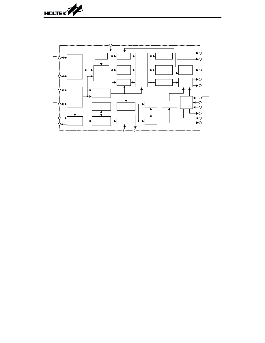
Block Diagram
HT9320
3
July 21, 1999
M / B
C 1
R 1
P O
H K S
H D I
K e y
C o l u m n
F S M
K e y
F u n c t i o n
E n c o d e r
E n c o d e r
C o n t r o l
W R M
C o u n t e r
A D D R L
K e y R o w
S R A M
D e b o u n c e
D i v i d e r
C l o c k
G e n e r a t o r
M / B
F l a s h
T i m e r
C h e c k
T o n e
E n c o d e r
C o n v e r t e r
M o d e I n
H D / H F
T o n e
O u t
P u l s e
O u t
X 1
X 2
D T M F
H F I
M O D E
H F O
H D O
D O U T
C L O C K
X M U T E
C 8
R 5
H S T
K e y t o n e
C i r c u i t
K T
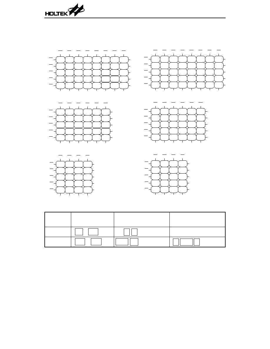
Keyboard Information
HT9320A/B/C/K/L
HT9320H
Memory dialing vs. keyboard form table
Dialing
Output
One-Touch
Memory Keyboard
Two-Touch
Memory Keyboard
Three-Touch
Memory Keyboard
M1~M10
M1 ~ M10
A
a (a=1~9, 0)
M11~M20
M11 ~ M20
PAGE Ma (Ma=M1~M10)
A PAGE a (a=1~9, 0)
HT9320
4
July 21, 1999
C 1
C 2
C 3
C 4
C 5
C 6
R 1
R 2
R 3
R 4
R 5
C 1
C 2
C 3
C 4
C 5
C 7
C 8
C 6
R 1
R 2
R 3
R 4
R 5
· O n e - t o u c h m e m o r y k e y b o a r d
· T w o - t o u c h m e m o r y k e y b o a r d
· T h r e e - t o u c h m e m o r y k e y b o a r d
R 1
R 2
R 3
R 4
R 5
C 1
C 2
C 3
C 4
P
2
5
8
0
M 1 6
M 1 7
M 1 8
M 1 9
M 2 0
M 6
M 7
M 8
M 9
M 1 0
M 1 1
M 1 2
M 1 3
M 1 4
M 1 5
M 1
M 2
M 3
M 4
M 5
3
6
9
#
S A
1
4
7
* / T
M 6 /
M 7 /
M 8 /
M 9 /
M 1 0 /
M 1 6
M 1 7
M 1 8
M 1 9
M 2 0
M 1 1
M 1 2
M 1 3
M 1 4
M 1 5
M 1 /
M 2 /
M 3 /
M 4 /
M 5 /
P
2
5
8
0
P A G E
3
6
9
#
S A
1
4
7
* / T
F
A
S T
R
F
S T
R
F
S T
R
P
2
5
8
0
P A G E
3
6
9
#
S A
1
4
7
* / T
C 1
C 2
C 3
C 4
C 5
C 6
R 1
R 2
R 3
R 4
R 5
C 1
C 2
C 3
C 4
C 5
C 7
C 8
C 6
R 1
R 2
R 3
R 4
R 5
· O n e - t o u c h m e m o r y k e y b o a r d
· T w o - t o u c h m e m o r y k e y b o a r d
· T h r e e - t o u c h m e m o r y k e y b o a r d
R 1
R 2
R 3
R 4
R 5
C 1
C 2
C 3
C 4
2
5
8
0
M 1 6
M 1 7
M 1 8
M 1 9
M 2 0
M 6
M 7
M 8
M 9
M 1 0
M 1 1
M 1 2
M 1 3
M 1 4
M 1 5
M 1
M 2
M 3
M 4
M 5
3
6
9
#
S A
1
4
7
*
M 6 /
M 7 /
M 8 /
M 9 /
M 1 0 /
M 1 6
M 1 7
M 1 8
M 1 9
M 2 0
M 1 1
M 1 2
M 1 3
M 1 4
M 1 5
M 1 /
M 2 /
M 3 /
M 4 /
M 5 /
2
5
8
0
P A G E
3
6
9
#
S A
1
4
7
*
P ® T
F
A
S T
R / P
2
5
8
0
P A G E
3
6
9
#
S A
1
4
7
*
P ® T
F
A
S T
R / P
P ® T
F
S T
R / P
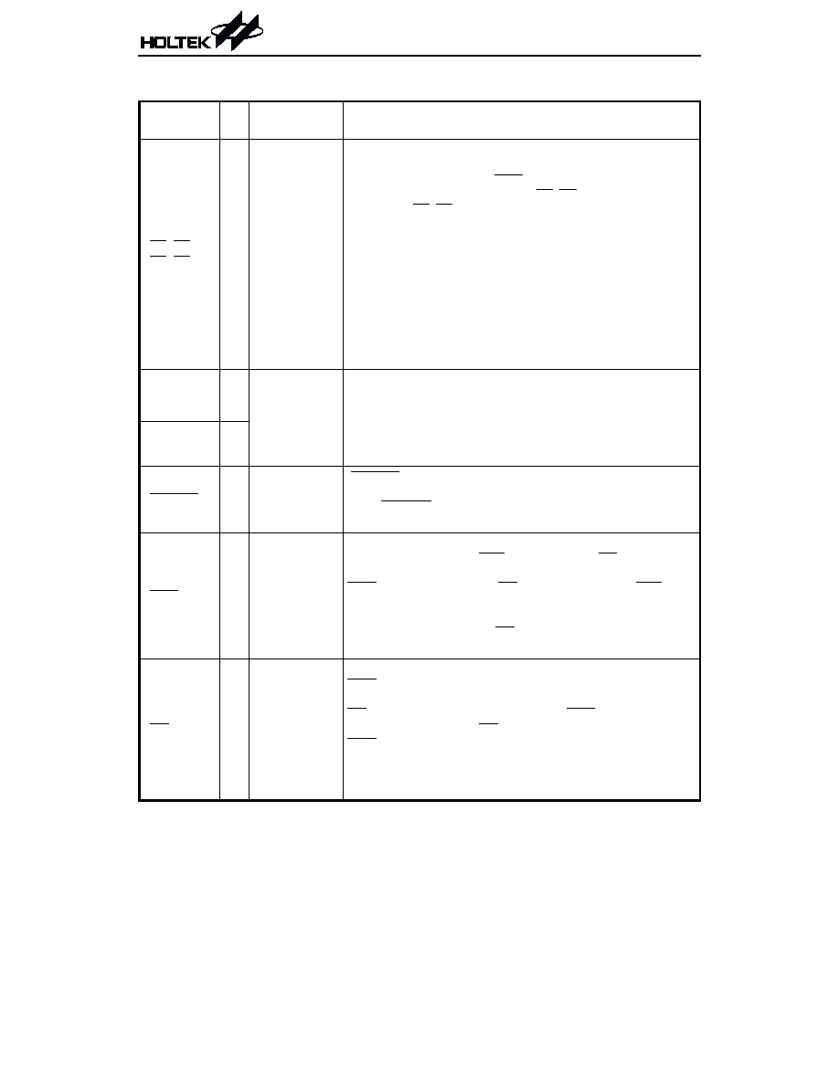
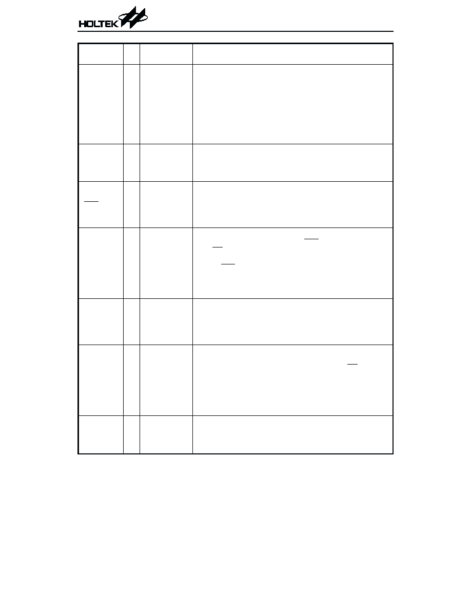
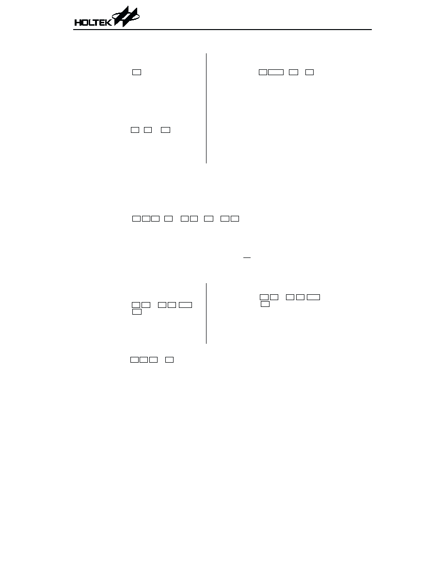
Pin Description
Pin Name I/O
Internal
Connection
Description
C1~C8
R1~R5
I/O
CMOS
IN/OUT
These pins form a 5´8 keyboard matrix which can perform
keyboard input detection and dialing specification setting
functions. When on-hook (HKS=high) all the pins are set high.
While off-hook the column group (C1~C8) remains low and the
row group (R1~R5) is set high for key input detection.
For the HT9320L-X, the column group remains high and the
row group is set low for key input detection.
An inexpensive single contact 5´8 keyboard can be used as an
input device. Pressing a key connects a single column to a sin-
gle row, and actuates the system oscillator that results in a di-
aling signal output. If more than two keys are pressed at the
same time, no response occurs. The key-in debounce time is
20ms. Refer to the keyboard information for keyboard ar-
rangement and to the functional description for dialing speci-
fication selection.
X1
I
OSCILLATOR
The system oscillator consists of an inverter, a bias resistor
and the necessary load capacitor on chip. Connecting a stan-
dard 3.579545MHz crystal or ceramic resonator to the X1 and
X2 terminals can implement the oscillator function. The oscil-
lator is turned off in the standby mode, and is actuated when-
ever a keyboard entry is detected.
X2
O
XMUTE
O
NMOS OUT
XMUTE is an NMOS open drain structure pulled to VSS dur-
ing dialing signal transmission. Otherwise, it is an open cir-
cuit. XMUTE is used to mute the speech circuit when
transmitting the dial signal.
HKS
I
CMOS IN
This pin is used to monitor the status of the hook-switch and its
combination with HFI/HDI can control the PO pin output to
makeorbreaktheline.
HKS=VDD:On-hookstate(PO=low).ExceptforHFI/HDI
(hand-free/hold-lineco ntrolinput),other
functionsarealldisabled.
HKS=VSS:Off-hookstate(PO=high).The chipisinthestand-
bymodeandreadytoreceivethekeyinput.
PO
O
CMOS OUT
This pin is a CMOS output structure which by receiving the
HKS and HFO/HDO signals, control the dialer to connect or
disconnect the telephone line.
PO outputs a low to break line when HKS is high (on-hook)
and HFO/HDO is low. PO outputs a high to make line when
HKS is low (off-hook) or HFO is high or HDO is high.
During the off-hook state, this pin also outputs the dialing
pulse train in pulse mode dialing. While in the tone mode, this
pin is always high.
HT9320
5
July 21, 1999
Pin Name I/O
Internal
Connection
Description
MODE
I/O
CMOS
IN/OUT
This is a three-state input/output pin, used for dialing mode
selection, either Tone mode or Pulse mode, 10pps/20pps
MODE=VDD: Pulse mode, 10pps
MODE=OPEN: Pulse mode, 20pps
MODE=VSS: Tone mode
During the pulse mode dialing, switching this pin to the tone
mode changes the subsequent digit entry to the tone mode.
When the chips are in tone mode, switching to the pulse mode
will also be recognized.
DTMF
O
CMOS OUT
This pin is active only when the chip transmits tone dialing
signals. Otherwise, it always outputs a low. The pin outputs
tone signals to drive the external transmitter amplifier cir-
cuit. The load resistor should not be less than 5kW.
HDI
I
CMOS IN
Pull-high
This pin is a schmitt trigger input structure. Active low. Ap-
plying a negative going pulse to this pin can toggle the HDO out-
put once.
An external RC network is recommended for input
debouncing. The pull-high resistance is 200kW typ.
HDO
O
CMOS OUT
The HDO is a CMOS output structure. Its output is toggle- con-
trolled by a negative transition on HDI. When HDO is toggled
high, PO keeps high to hold the line. The hold function can be re-
leased by setting HFO high or by an on-off hook operation or by
another HDI input. The HDO pin can directly drive the HT3810
series melody generator to produce a hold-line background mel-
ody. Refer to the functional description for the hold-line func-
tion.
HFI
I
CMOS IN
Pull-low
This pin is a schmitt trigger input structure. Active high. Ap-
plying a positive going pulse to HFI can toggle the HFO once
and hence control the hand-free function.
An external RC network is recommended for input
debouncing. The pull-low resistance of HFI is 200kW typ.
HFO
O
CMOS OUT
The HFO is a CMOS output structure. Its output is toggle-
controlled by a positive transition on the HFI pin. When HFO
is high, the hand-free function is enabled and PO outputs a
high to connect the line.
The hand-free function can be released by an on-off-hook oper-
ation or by another HFI input or by setting HDO high. Refer to
the functional description for the hand-free function opera-
tion.
DOUT
O
NMOS OUT
NMOS open drain output pin. It outputs the BCD code of the
dialing digits to the LCD driver chip (HT16XX series) or mC for
dialing number display. Refer to the functional description for
the detailed timing.
HT9320
6
July 21, 1999
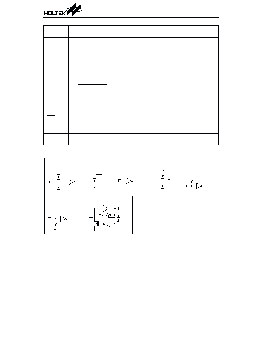
Pin Name I/O
Internal
Connection
Description
CLOCK
O
NMOS OUT
NMOS open drain output. When dialing, it outputs a series of
pulse trains for DOUT data synchronization. DOUT data is
valid at the falling edge of clock.
VDD
I
¾
Positive power supply, 2.0V~5.5V for normal operation
VSS
I
¾
Negative power supply
HST
I
CMOS IN
Pull-low
(HT9320A)
On-hook store enable input
HST=VDD: On-hook store (HT9320A/H)
HST=Floating: Off-hook store (HT9320A)
HST=VSS: Off-hook store (HT9320H)
The Pull-low resistance is 200kW typ.
CMOS IN
(HT9320H)
M/B
I
CMOS IN
Pull-high
(HT9320A)
Make/Break ratio selection
M/B=VSS: 33.3/66.6 (HT9320A)
M/B=Floating: 40/60 (HT9320A)
M/B=VDD: 33.3/66.6 (HT9320H)
M/B=VSS: 40/60 (HT9320H)
The pull-high resistance is 200kW typ.
CMOS IN
(HT9320H)
KT
O
CMOS OUT
Keytone output pin. Outputs a 1.2kHz tone carrier for 34ms
each time a key is pressed in the pulse mode.
Approximate internal connection circuits
HT9320
7
July 21, 1999
N M O S O U T
V D D
C M O S I N / O U T
C M O S O U T
C M O S I N
P u l l - l o w
C M O S I N
P u l l - h i g h
C M O S I N
O S C I L L A T O R
X 1
X 2
E N
1 0 M
2 0 p F
1 0 p F
V D D
Absolute Maximum Ratings
Supply Voltage ................................-0.3V to 6V
Storage Temperature ................-50°C to 125°C
Input Voltage .................. V
SS
-0.3 to V
DD
+0.3V
Operating Temperature .............-20°C to 75°C
Note: These are stress ratings only. Stresses exceeding the range specified under ²Absolute Maxi-
mum Ratings² may cause substantial damage to the device. Functional operation of this device
at other conditions beyond those listed in the specification is not implied and prolonged expo-
sure to extreme conditions may affect device reliability.
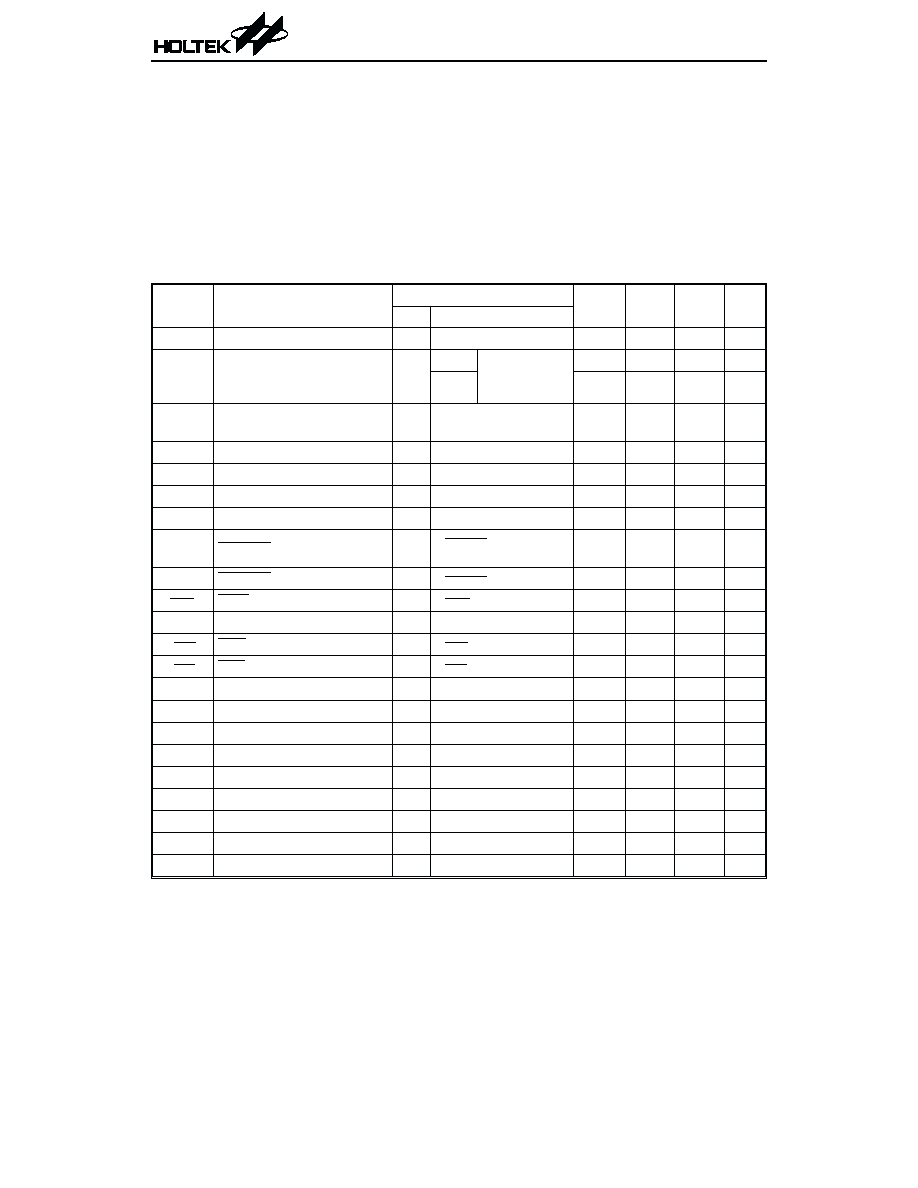
Electrical Characteristics
f
OSC
=3.5795MHz, Ta=25°C
Symbol
Parameter
Test Conditions
Min.
Typ.
Max. Unit
V
DD
Conditions
V
DD
Operating Voltage
¾
¾
2
¾
5.5
V
I
DD
Operating Current
2.5V
Pulse Off-hook
Keypad entry
No load
¾
0.2
1
mA
Tone
¾
0.6
2
mA
I
STB
Standby Current
1V On-hook, no load
No entry
¾
¾
1
mA
V
R
Memory Retention Voltage
¾
¾
1
¾
5.5
V
I
R
Memory Retention Current 1V On-hook
¾
0.1
0.2
mA
V
IL
Input Low Voltage
¾
¾
V
SS
¾
0.2V
DD
V
V
IH
Input High Voltage
¾
¾
0.8V
DD
¾
V
DD
V
I
XMO
XMUTE Leakage Current
¾
V
XMUTE
=12V
No entry
¾
¾
1
mA
I
OLXM
XMUTE Sink Current
2.5V V
XMUTE
=0.5V
1
¾
¾
mA
I
HKS
HKS Pin Input Current
2.5V V
HKS
=2.5V
¾
¾
0.1
mA
R
HFI
HFI Pull-low Resistance
2.5V V
HFI
=2.5V
¾
200
¾
kW
R
HDI
HDI Pull-high Resistance
2.5V V
HDI
=0V
¾
200
¾
kW
R
M/B
M/B Pull-high Resistance
2.5V V
M/B
=0V
¾
200
¾
kW
R
HST
HST Pull-low Resistance
2.5V V
HST
=2.5V
¾
200
¾
kW
I
OH1
Keypad Pin Source Current 2.5V V
OH
=0V
-4
¾
-40
mA
I
OL1
Keypad Pin Sink Current
2.5V V
OL
=2.5V
200
400
¾
mA
I
OH2
HFO Pin Source Current
2.5V V
OH
=2V
-1
¾
¾
mA
I
OL2
HFO Pin Sink Current
2.5V V
OL
=0.5V
1
¾
¾
mA
I
OH3
HDO Pin Source Current
2.5V V
OH
=2V
-1
¾
¾
mA
I
OL3
HDO Pin Sink Current
2.5V V
OL
=0.5V
1
¾
¾
mA
I
OH4
KT Pin Source Current
2.5V V
OH
=2V
-1
¾
¾
mA
I
OL4
KT Pin Sink Current
2.5V V
OL
=0.5V
1
¾
¾
mA
HT9320
8
July 21, 1999
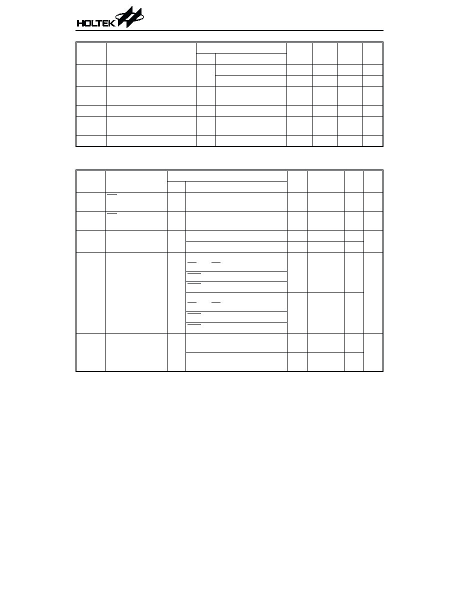
Symbol
Parameter
Test Conditions
Min.
Typ.
Max. Unit
V
DD
Conditions
T
FP
Pause Time After Flash
¾
Control key
¾
0.2
¾
s
Digit key
¾
1
¾
s
T
RP
Pause Time for One-key
Redialing
¾
One-key redialing
¾
1
¾
s
T
DB
Key-in Debounce Time
¾
¾
¾
20
¾
ms
T
BRK
Break Time for One-key
Redialing
¾
One-key redialing
¾
1.2
¾
s
f
OSC
System Frequency
¾
Crystal=3.5795MHz 3.5759 3.5795 3.5831 MHz
Pulse Mode Electrical Characteristics
f
OSC
=3.5795MHz, Ta=25°C
Symbol
Parameter
Test Conditions
Min.
Typ.
Max. Unit
V
DD
Conditions
I
POH
PO Output Source
Current
2.5V V
OH
=2V
-0.2
¾
¾
mA
I
POL
PO Output Sink
Current
2.5V V
OL
=0.5V
0.2
0.6
¾
mA
PR
Pulse Rate
¾
MODE pin is connected to V
DD
¾
10
¾
pps
MODE pin is opened
¾
20
¾
M/B
Make/Break Ratio
¾
A resistor is linked between
R2 and C1 (HT9320B/C/K/L)
¾
33:66
¾
%
M/B=VSS (HT9320A)
M/B=VDD (HT9320H)
No resistor is linked between
R2 and C1 (HT9320B/C/K/L)
¾
40:60
¾
M/B=Floating (HT9320A)
M/B=VSS (HT9320H)
T
PDP
Pre-digit-pause
Time
¾
M/B ratio=40:60
¾
40 (10pps)
20 (20pps)
¾
ms
M/B ratio=33:66
¾
33 (10pps)
17 (20pps)
¾
HT9320
9
July 21, 1999
Symbol
Parameter
Test Conditions
Min.
Typ.
Max. Unit
V
DD
Conditions
T
IDP
Inter-digit-pause
Time
¾
Pulse rate=10pps. No resistor
is linked between R1 and C5
(HT9320A/B/C/K)
¾
800
¾
ms
Pulse rate=10pps (HT9320H/L)
Pulse rate=10pps. A resistor
is linked between R1 and C5
(HT9320A/B/C/K)
¾
400
¾
Pulse rate=20pps
¾
500
¾
T
M
Pulse Make
Duration
¾
A resistor is linked between
R2 and C1 (HT9320B/C/K/L)
¾
33 (10pps)
17 (20pps)
¾
ms
M/B=VSS (HT9320A)
M/B=VDD (HT9320H)
No resistor is linked between
R2 and C1 (HT9320B/C/K/L)
¾
40 (10pps)
20 (20pps)
¾
M/B=Floating (HT9320A)
M/B=VSS (HT9320H)
T
B
pulse Break
Duration
¾
A resistor is linked between
R2 and C1 (HT9320B/C/K/L)
¾
66 (10pps)
33 (20pps)
¾
ms
M/B=VSS (HT9320A)
M/B=VDD (HT9320H)
No resistor is linked between
R2 and C1 (HT9320B/C/K/L)
¾
60 (10pps)
30 (20pps)
¾
M/B=Floating (HT9320A)
M/B=VSS (HT9320H)
T
KT
Keytone Duration
¾ Pulse mode (HT9320K)
¾
34
¾
ms
F
KTC
Keytone Carrier
¾ Pulse mode (HT9320K)
¾
1.2
¾
kHz
Tone Mode Electrical Characteristics
f
OSC
=3.5795MHz, Ta=25°C
Symbol
Parameter
Test Conditions
Min.
Typ. Max. Unit
V
DD
Conditions
V
TDC
DTMF Output DC Level
¾
¾
0.45V
DD
¾
0.7V
DD
V
I
TOL
DTMF Sink Current
2.5V V
DTMF
=0.5V
0.1
¾
¾
mA
V
TAC
DTMF Output AC Level
¾ Row group, R
L
=5kW
0.12
0.155 0.18
Vrms
R
L
DTMF Output Load
2.5V THD£-23dB
5
¾
¾
kW
A
CR
Column Pre-emphasis
2.5V Row group=0dB
1
2
3
dB
HT9320
10
July 21, 1999
Symbol
Parameter
Test Conditions
Min.
Typ. Max. Unit
V
DD
Conditions
THD
Tone Signal Distortion
2.5V R
L
=5kW
¾
-30
-23
dB
T
TMIN
Minimum Tone Duration
¾ Auto-redial
¾
82.5
¾
ms
T
ITPM
Minimum Inter-tone Pause
¾ Auto-redial
¾
85.5
¾
ms
THD (Distortion) (dB) = 20 log ( V1
V2
Vn / Vi
Vh
2
2
2
2
2
+
+
+
K
)
Vi, Vh: Row group and column group signals
V1, V2, ... Vn: Harmonic signals (BW=300Hz~3500Hz)
HT9320
11
July 21, 1999
Functional Description
Keyboard matrix
C1~C8 and R1~R5 form a keyboard matrix. To-
gether with a standard 5´8 keyboard, the key-
board matrix is used for dialing entries. In
addition, the keyboard matrix also provides resis-
tor options for different dialing specification se-
lections. The keyboard arrangement for the
HT9320 series are shown in the Keyboard In-
formation.
Tone frequency
Tone
Name
Output
Frequency (Hz)
% Error
Specified Actual
R2
697
699
+0.29%
R3
770
766
-0.52%
R4
852
847
-0.59%
R5
941
948
+0.74%
C1
1209
1215
+0.50%
C2
1336
1332
-0.30%
C3
1477
1472
-0.34%
Note:%Errordoesnotcontainthecrystalfrequency
drift
Dialing specification selection
Various dialing specifications can be selected by
adding resistors across keyboard matrix pins.
The allowable option resistor connections are
shown on the table.
All the resistors are 330kW. The resistor option
functions and the default specifications (with-
outoptionresistors)arelistedbelow(HT9320A/
B/C/K/L).
Option
Resistor
Option
Function
Default
(No Resistor)
R
K12
(HT9320B/
C/K/L)
Ratio Selection
40:60
R
K13
Flash Function
/Time Selection
Flash= control
function
Flash time=
600ms
R
K14
R
K21
Pause & P®T
Duration
Selection
T
P
= 3.6s
T
P®T
= 3.6s
R
K31
Pulse Number
Selection
N
R
K41
R
K51
(HT9320A
/B/C/K)
Inter-digit-
Pause Time for
10pps
800ms
R 1
R 2
R 3
R 4
K 2 1
R
C 1
C 2
C 3
C 4
C 5
C 6
C 7
K 3 1
R
K 4 1
R
K 5 1
R
K 6 1
R
K 7 1
R
K 1 2
R
K 1 3
R
K 1 4
R
HT9320
12
July 21, 1999
Option
Resistor
Option
Function
Default
(No Resistor)
R
K51
R
K61
R
K71
(HT9320L)
International
Direct Dialing
Lock Selection
Normal dialing
(unlock)
M/B ratio selection table
·
HT9320A
M/B Pin
M/B Ratio (%)
VSS
33.3:66.6
Floating
40:60
·
HT9320B/C/K/L
R
K12
M/B Ratio (%)
No
40:60
Yes
33.3:66.6
·
HT9320H
M/B Pin
M/B Ratio (%)
VDD
33.3:66.6
VSS
40:60
Flash function/time (duration) selection table
·
HT9320A/B/C/K/L
R
K13
R
K14
Flash
Function
Flash
Time (T
F
)
No
No
Control
600ms
No
Yes
Digit
600ms
Yes
No
Digit
98ms
Yes
Yes
Digit
300ms
·
HT9320H
M/B Pin
Flash
Function
Flash Time
(T
F
)
VSS
Digit
600ms
VDD
Digit
100ms
Pause and P®T duration selection table
·
HT9320A/B/C/K/L
R
K21
T
P
(sec)
T
P®T
(sec)
No
3.6
3.6
Yes
2
1
·
HT9320H
T
P
(sec)
T
P®T
(sec)
3.6
3.6
Pulse number selection table
·
HT9320A/B/C/K/L
R
K31
R
K41
Pulse
Number
No
No
N
No
Yes
N+1
Yes
No
10-N
Yes
Yes
¾
·
HT9320H
Pulse Number
N
Inter-digit-pause time for 10pps
·
HT9320A/B/C/K
R
K51
Inter-digit pause time
No
800ms
Yes
400ms
·
HT9320H/L
Inter-digit pause time
800ms
HT9320
13
July 21, 1999
Pulse number table
Keypad
Output Pulse Number
Digit Key
N
10-N
N+1
1
1
9
2
2
2
8
3
3
3
7
4
4
4
6
5
5
5
5
6
6
6
4
7
7
7
3
8
8
8
2
9
9
9
1
10
0
10
10
1
*/T
P®T
P®T
P®T
#
Ignored
Ignored
Ignored
DOUT BCD code
When dialing, the corresponding 4-bit BCD
codes are serially presented on DOUT from
MSB to LSB. The data of DOUT is valid at the
falling edge of the CLOCK pin. The following
table lists the BCD codes corresponding to the
keyboard input.
Key-In BCD Code Key-In BCD Code
1
0001
8
1000
2
0010
9
1001
3
0011
0
1010
4
0100
*/T
1101
5
0101
#
1100
6
0110
F
1011
7
0111
P
1110
On hook store (HT9320A/H)
When the external power supply (2V~5.5V) is
used and the HST pin is connected to VDD, the
user can store dialing numbers to the memories
(M1~M20) during on-hook state.
On/Off hook store selection table
HST Pin
Hook Store Mode
VDD (HT9320A/H)
On-hook store
Floating (HT9320A)
Off-hook store
VSS (HT9320H)
Off-hook store
Lock function (HT932L)
This function aims to detect lock dialing num-
bers to prevent from an unauthorized long dis-
tance call. The dialing output of this chip is
disabled if the first input key after on-off hook is
the lock number when the lock function is en-
abled.
International direct dialing lock (IDD lock) se-
lection table
R
K51
R
K61
R
K71
Lock Function
No
No
No Normal dialing without
lock function
No
No
Yes To lock 0
No
Yes
¾
To lock 0, 9
Yes
¾
¾
IDD lock operation by the
telephone keyboard.
(See keyboard operation)
Note: ²¾² stands for ²don¢t care²
Hand-free function operation
·
Hand-free function execution
When HFO is low, a rising edge triggers the
HFI, enabling the Hand-free function (HFO
becomes high).
·
Reset Hand-free function
When HFO is high, the Hand-free function is
enabled and can be reset by:
¨
Off-hook
¨
Applying a rising edge to HFI
¨
Changing the HDO pin from low to high
HT9320
14
July 21, 1999
·
Hand-free function table
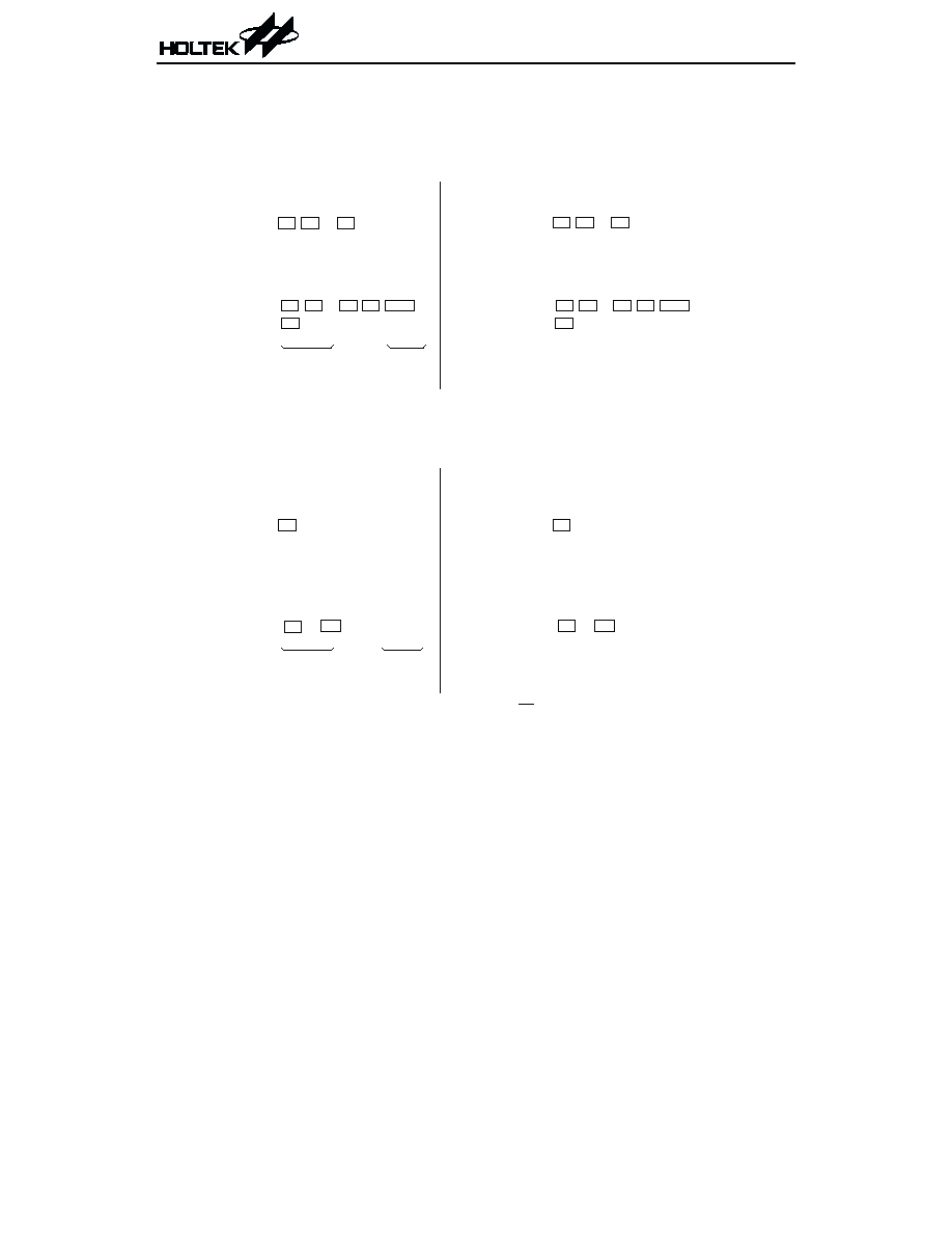
Hold-line function operation
·
Hold-line function execution
When HDO is low, a falling edge triggers the
HDI, enabling the Hold-line function (HDO
becomes high). The XMUTE remains low
when HDO is high.
·
Reset Hold-line function
When HDO is high, the Hold-line function is
enabled and can be reset by:
¨
Off-hook
¨
Applying a falling edge to HDI
¨
Changing the HFO pin from low to high
·
Hold-line function table
Key definition
·
0,1,2,3,4,5,6,7,8,9 keys
These are dialing number input keys for both
the pulse mode and the tone mode operations.
·
*/T
This key executes the P®T function and wait
a T
P®T
duration in the pulse mode. On the
other hand, the */T key executes the * func-
tion in the tone mode.
·
* (HT9320H)
The * key executes the * tone output function
in the tone mode. No response in the pulse
mode.
·
P®T
The key executes the P®T function in the
pulse mode. No response in the tone mode.
·
#
This is a dialing signal key for the tone mode
only, no response in the pulse mode.
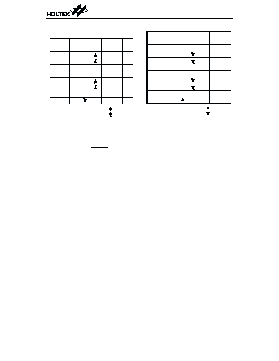
C u r r e n t S t a t e
I n p u t
N e x t S t a t e
H K S
H
H
H
H
L
L
L
L
X
H F O
L
L
H
X
L
L
H
X
X
H D O
X
X
X
L
X
X
L
X
L
H F I
L
L
L
L
L
H K S
A n
A n
A n
L
A n
A n
A n
H
A n
H F O
L
H
L
L
L
H
L
A n
L
H D O
A n
L
A n
L
A n
L
A n
A n
H
H D I
H
H
H
H
H
H
H
H
H :
L :
L o g i c H I G H
L o g i c L O W
X :
A n :
D o n ' t c a r e
U n c h a n g e d
:
:
R i s i n g e d g e
F a l l i n g e d g e
C u r r e n t S t a t e
I n p u t
N e x t S t a t e
H K S
H
H
H
H
L
L
L
L
X
H D O
L
L
H
X
L
L
H
X
X
H F O
X
X
L
X
X
X
L
X
L
H D I
H
H
H
H
H
H K S
A n
A n
A n
L
A n
A n
A n
H
A n
H D O
L
H
L
L
L
H
L
A n
L
H F O
A n
L
A n
L
A n
L
A n
A n
H
H F I
L
L
L
L
L
L
L
L
H :
L :
L o g i c H I G H
L o g i c L O W
X :
A n :
D o n ' t c a r e
U n c h a n g e d
:
:
R i s i n g e d g e
F a l l i n g e d g e

HT9320
15
July 21, 1999
·
SA
Pressing this key can save the preceding dial-
ing telephone numbers. The saved number is
redialed if it is pressed again. SAwill also redial
the saved number if it is the first key pressed at
the off-hook state. During the dialing signal
transmission, the SA key is inhibited.
·
F
The flash key can be selected as a digit or as a
control key by the option resistors R
K13
& R
K14.
Pressing the flash key will force the PO pin to
be ²low² for the T
F
duration and is then fol-
lowed by T
FP
(sec). T
F
can also be selected by
R
K13
, R
K14
.
·
P
Pause key. The execution of this key can
pause the output for the T
P
duration. T
P
can
be selected by R
K21
.
·
R
Redial key. Executes redialing as well as
one-key redial function.
·
R/P
Redial and pause function key. If it is pressed
as the first key after off-hook, this key exe-
cutes the redial function. Otherwise, it works
as the pause key.
·
ST
Store key. The execution of this key actuates
the store memory function with (or without)
dialing output. During the dialing signal
transmission, the ST key is inhibited.
·
A
Auto key. When this key is pressed before
pressing any one of the digital keys (0~9) it
executes the two-touch/ three-touch memory
dialing function.
·
PAGE
M11~M20 are represented by pressing the
PAGE key an.d the digital keys (0~9) or
M1~M10. That is to say, A PAGE digit key
(0~9) or PAGE®M1~M10 executes M11~M20
memorydialing.
·
M1~M20
One-touch memory dialing for speed-dialing
in either pulse or tone mode.
Keyboard operation
The following operations are described under an on-off-hook or on-hook condition with the hand-free active
condition.
HT9320
16
July 21, 1999
- P u l s e m o d e
( a ) w i t h o u t * / T
D i a l i n g o u t p u t : D 1 D 2 . . . D n
R M : D 1 D 2 . . . D n
S A M : U n c h a n g e d
( b ) w i t h * / T
D i a l i n g o u t p u t : D 1 D 2 . . . D n T
P ® T
D n + 1 . . . D m
R M : D 1 D 2 . . . D n * / T D n + 1 . . . D m
S A M : U n c h a n g e d
T o n e
P u l s e
K e y b o a r d i n p u t : D 1 D 2 . . . D n * / T D n + 1 . . .
· N o r m a l d i a l i n g
D m
( a ) w i t h o u t * / T
D i a l i n g o u t p u t : D 1 D 2 . . . D n
R M : D 1 D 2 . . . D n
S A M : U n c h a n g e d
( b ) w i t h * / T
D i a l i n g o u t p u t : D 1 D 2 . . . D n * D n + 1 . . . D m
R M : D 1 D 2 . . . D n * D n + 1 . . . D m
S A M : U n c h a n g e d
- T o n e m o d e
K e y b o a r d i n p u t : D 1 D 2 . . . D n
( a ) w i t h o u t * / T , P ® T
D i a l i n g o u t p u t : D 1 D 2 . . . D n
R M : U n c h a n g e d
S A M : U n c h a n g e d
R M c o n t e n t : D 1 D 2 . . . D n
( b ) w i t h * / T
D i a l i n g o u t p u t : D 1 D 2 . . . D n T
P ® T
D n + 1 . . . D m
R M : U n c h a n g e d
S A M : U n c h a n g e d
R M c o n t e n t : D 1 D 2 . . . D n * / T D n + 1 . . . D m
D i a l i n g o u t p u t : D 1 D 2 . . . D n
R M : U n c h a n g e d
S A M : U n c h a n g e d
R M c o n t e n t : D 1 D 2 . . . D n
( b ) w i t h * / T
D i a l i n g o u t p u t : D 1 D 2 . . . D n * D n + 1 . . . D m
R M : U n c h a n g e d
S A M : U n c h a n g e d
R M c o n t e n t : D 1 D 2 . . . D n * / T D n + 1 . . . D m
- P u l s e m o d e
- T o n e m o d e
K e y b o a r d i n p u t : R
( a ) w i t h o u t * / T , P ® T
K e y b o a r d i n p u t : R
P u l s e
T o n e
· R e d i a l
N o t e : T h e m a x i m u m c a p a c i t y o f t h e R M m e m o r y i s 3 2 d i g i t s . W h e n m o r e t h a n 3 2 d i g i t s a r e e n t e r e d , t h e s i g n a l i s
t r a n s m i t t e d b u t t h e r e d i a l f u n c t i o n i s i n h i b i t e d .
K e y b o a r d i n p u t : D 1 D 2 . . . D n * / T D n + 1 . . .
D m
K e y b o a r d i n p u t : D 1 D 2 . . . D n
K e y b o a r d i n p u t : [ R o r R / P ]
K e y b o a r d i n p u t : [ R o r R / P ]
N o t e : I f t h e d i a l i n g n u m b e r e x c e e d s 3 2 d i g i t s , r e d i a l i n g i s i n h i b i t e d a n d P O = V D D
HT9320
17
July 21, 1999
K e y b o a r d i n p u t : D 1 D 2 . . . D n * / T D n + 1 . . .
D m
R
K e y b o a r d i n p u t : D 1 D 2 . . . D n * / T D n + 1 . . .
D m S A
( a ) w i t h o u t * / T
D i a l i n g o u t p u t : D 1 D 2 . . . D n T
B R K
T
R P
R M : D 1 D 2 . . . D n
S A M : U n c h a n g e d
( b ) w i t h * / T
R M : D 1 D 2 . . . D n * / T D n + 1 . . . D m
S A M : U n c h a n g e d
( a ) w i t h o u t * / T
R M : D 1 D 2 . . . D n
S A M : U n c h a n g e d
( b ) w i t h * / T
- T o n e m o d e
- P u l s e m o d e
P u l s e
T
B R K
T
R P
D 1 D 2 . . . D n T
P T
P u l s e
D i a l i n g o u t p u t : D 1 D 2 . . . D n * D n + 1 . . . D m
R M : D 1 D 2 . . . D n * D n + 1 . . . D m
S A M : U n c h a n g e d
T
B R K
T
R P
D 1 D 2 . . . D n * D n + 1
. . . D m
P u l s e
T o n e
D i a l i n g o u t p u t : D 1 D 2 . . . D n T
P ® T
D n + 1 . . . D m
T o n e
· O n e - k e y r e d i a l
K e y b o a r d i n p u t : D 1 D 2 . . . D n R
K e y b o a r d i n p u t : D 1 D 2 . . . D n R
( a ) w i t h o u t * / T
D i a l i n g o u t p u t : D 1 D 2 . . . D n
R M : D 1 D 2 . . . D n
S A M : D 1 D 2 . . . D n
( b ) w i t h * / T
R M : D 1 D 2 . . . D n * / T D n + 1 . . . D m
S A M : D 1 D 2 . . . D n * / T D n + 1 . . . D m
( a ) w i t h o u t * / T
D i a l i n g o u t p u t : D 1 D 2 . . . D n
R M : D 1 D 2 . . . D n
S A M : D 1 D 2 . . . D n
( b ) w i t h * / T
D i a l i n g o u t p u t : D 1 D 2 . . . D n * D n + 1 . . . D m
R M : D 1 D 2 . . . D n * D n + 1 . . . D m
S A M : D 1 D 2 . . . D n * D n + 1 . . . D m
- P u l s e m o d e
- T o n e m o d e
K e y b o a r d i n p u t : D 1 D 2 . . . D n S A
D i a l i n g o u t p u t : D 1 D 2 . . . D n T
P ® T
D n + 1 . . . D m
T o n e
P u l s e
· S A c o p y
K e y b o a r d i n p u t : D 1 D 2 . . . D n S A
D i a l i n g o u t p u t : D 1 D 2 . . . D n T
P
D n + 1 . . . D m
R M : D 1 D 2 . . . D n P D n + 1 . . . D m
S A M : U n c h a n g e d
· P a u s e
D 1 D 2 . . . D n
P u l s e
D i a l i n g o u t p u t : D 1 D 2 . . . D n T
B R K
T
R P
D 1 D 2
. . . D n
D n + 1 . . . D m
K e y b o a r d i n p u t : D 1 D 2 . . . D n * / T D n + 1 . . .
D m S A
N o t e : T h e m a x i m u m c a p a c i t y o f t h e R M m e m o r y i s 3 2 d i g i t s . W h e n m o r e t h a n 3 2 d i g i t s p l u s t h e " S A " k e y
a r e e n t e r e d , t h e S A V E f u n c t i o n w i l l n o t b e e x e c u t e d , a n d a l l t h e e x i s t i n g d a t a i n t h e s a v e m e m o r y
w i l l n o t b e c h a n g e d .
K e y b o a r d i n p u t : D 1 D 2 . . . D n * / T D n + 1 . . .
D m
R
K e y b o a r d i n p u t : D 1 D 2 . . . D n [ P o r R / P ] D n + 1 . . . D m
N o t e : I f t h e d i a l i n g n u m b e r e x c e e d s 3 2 d i g i t s , r e d i a l i n g i s i n h i b i t e d a n d P O = V D D
HT9320
18
July 21, 1999
( a ) w i t h o u t * / T
D i a l i n g o u t p u t : D 1 D 2 . . . D n
R M : U n c h a n g e d
S A M : U n c h a n g e d
( b ) w i t h * / T
R M : U n c h a n g e d
S A M : U n c h a n g e d
( a ) w i t h o u t * / T
D i a l i n g o u t p u t : D 1 D 2 . . . D n
R M : U n c h a n g e d
S A M : U n c h a n g e d
( b ) w i t h * / T
D i a l i n g o u t p u t : D 1 D 2 . . . D n * D n + 1 . . . D m
R M : U n c h a n g e d
S A M : U n c h a n g e d
S A M c o n t e n t : D 1 D 2 . . . D n
S A M c o n t e n t : D 1 D 2 . . . D n * / T D n + 1 . . . D m
S A M c o n t e n t : D 1 D 2 . . . D n
S A M c o n t e n t : D 1 D 2 . . . D n * D n + 1 . . . D m
- P u l s e m o d e
- T o n e m o d e
D i a l i n g o u t p u t : D 1 D 2 . . . D n T
P ® T
D n + 1 . . . D m
T o n e
P u l s e
· S A d i a l i n g
K e y b o a r d i n p u t : S A
K e y b o a r d i n p u t : S A
K e y b o a r d i n p u t : S A
K e y b o a r d i n p u t : S A
D i a l i n g o u t p u t :
M a : D 1 D 2 . . . D n
R M : D 1 D 2 . . . D n
- O n e - t o u c h m e m o r y s t o r e w i t h o u t d i a l i n g o u t p u t
S A M : U n c h a n g e d
D i a l i n g o u t p u t : D 1 D 2 . . . D n
M a : D 1 D 2 . . . D n
R M : D 1 D 2 . . . D n
- O n e - t o u c h m e m o r y s t o r e w i t h d i a l i n g o u t p u t
S A M : U n c h a n g e d
K e y b o a r d i n p u t : D 1 D 2 . . . D n S T S T M a
D i a l i n g o u t p u t :
M a : D 1 D 2 . . . D n ( a = b + 1 0 , M 1 0 = M 0 )
R M : D 1 D 2 . . . D n
T h r e e - t o u c h m e m o r y s t o r e w i t h o u t d i a l i n g o u t p u t
( M 1 1 ~ M 2 0 )
S A M : U n c h a n g e d
D i a l i n g o u t p u t :
M b : D 1 D 2 . . . D n
R M : D 1 D 2 . . . D n
S A M : U n c h a n g e d
D i a l i n g o u t p u t : D 1 D 2 . . . D n
M b : D 1 D 2 . . . D n
R M : D 1 D 2 . . . D n
S A M : U n c h a n g e d
· M e m o r y s t o r e
K e y b o a r d i n p u t : S T D 1 D 2 . . . D n S T M a
D i a l i n g o u t p u t : D 1 D 2 . . . D n
M a : D 1 D 2 . . . D n ( a = b + 1 0 , M 1 0 = M 0 )
R M : D 1 D 2 . . . D n
- T h r e e - t o u c h m e m o r y s t o r e w i t h d i a l i n g o u t p u t
( M 1 1 ~ M 2 0 )
S A M : U n c h a n g e d
- T w o - t o u c h m e m o r y s t o r e w i t h d i a l i n g o u t p u t
( M 1 ~ M 1 0 )
N o t e : I f t h e d i a l i n g n u m b e r e x c e e d s 3 2 d i g i t s , t h e m e m o r y s t o r e i s i n h i b i t e d .
H o w e v e r , i f t h e d i a l i n g n u m b e r i s n o t m o r e t h a n 3 2 d i g i t s t h e m e m o r y w i l l s t o r e a m a x . o f 1 6 d i g i t s .
M a = M 1 ~ M 2 0 , M b = M 1 ~ M 1 0 , a = 1 ~ 2 0 , b = 1 ~ 9 , 0
M a : D 1 D 2 . . . D n ( a = b + 1 0 , M 1 0 = M 0 )
K e y b o a r d i n p u t : S T D 1 D 2 . . . D n S T
[ b o r M b ]
K e y b o a r d i n p u t : S T D 1 D 2 . . . D n S T
P A G E [ b o r M b ]
( M 1 1 ~ M 2 0 )
- T w o - t o u c h m e m o r y s t o r e w i t h o u t d i a l i n g o u t p u t
( M 1 ~ M 1 0 )
M a : D 1 D 2 . . . D n ( a = b + 1 0 , M 1 0 = M 0 )
[ b o r M b ]
P A G E [ b o r M b ]
( M 1 1 ~ M 2 0 )
K e y b o a r d i n p u t : S T D 1 D 2 . . . D n S T
P A G E [ b o r M b ]
P A G E [ b o r M b ]
K e y b o a r d i n p u t : D 1 D 2 . . . D n S T S T
K e y b o a r d i n p u t : D 1 D 2 . . . D n S T S T
K e y b o a r d i n p u t : D 1 D 2 . . . D n S T S T
HT9320
19
July 21, 1999
R M : D 1 D 2 . . . D n
S A M : U n c h a n g e d
F l a s h a s a d i g i t a l k e y
K e y b o a r d i n p u t : D 1 D 2 . . . D n F D n + 1 . . .
D m
D i a l i n g o u t p u t : D 1 D 2 D 3 D 1 D 2 . . . D n D n + 1 . . . D m
M 1 / M 2 : U n c h a n g e d
R M : D 1 D 2 D 3 D 1 D 2 . . . D n D n + 1 . . . D m
M 2 c o n t e n t : D n + 1 . . . D m
M 1 c o n t e n t : D 1 D 2 . . . D n
S A M : U n c h a n g e d
K e y b o a r d i n p u t : D 1 D 2 D 3 [ M 1 o r A 1 ] [ M 2 o r A 2 ]
D i a l i n g o u t p u t : D 1 D 2 . . . D n
M a : U n c h a n g e d
R M : D 1 D 2 . . . D n
- O n e - t o u c h m e m o r y d i a l i n g ( M 1 ~ M 2 0 )
S A M : U n c h a n g e d
M a c o n t e n t : D 1 D 2 . . . D n
K e y b o a r d i n p u t : M a
D i a l i n g o u t p u t : D 1 D 2 . . . D n
M b : U n c h a n g e d
R M : D 1 D 2 . . . D n
- T w o - t o u c h m e m o r y d i a l i n g ( M 1 ~ M 1 0 )
S A M : U n c h a n g e d
M b c o n t e n t : D 1 D 2 . . . D n
K e y b o a r d i n p u t : A [ b o r M b ]
D i a l i n g o u t p u t : D 1 D 2 . . . D n
M a : U n c h a n g e d ( a = b + 1 0 , M 1 0 = M 0 )
R M : D 1 D 2 . . . D n
- T h r e e - t o u c h m e m o r y d i a l i n g ( M 1 1 ~ M 2 0 )
S A M : U n c h a n g e d
M 1 1 c o n t e n t : D 1 D 2 . . . D n
K e y b o a r d i n p u t : A P A G E [ M b o r b ]
- F l a s h a s a c o n t r o l k e y
( a ) T h e i n t e r v e n i e n t k e y
R M : U n c h a n g e d
S A M : U n c h a n g e d
D i a l i n g o u t p u t : T
F
T
F P
D 1 D 2 D n
K e y b o a r d i n p u t : F D 1 D 2 . . . D n
( b ) T h e f i r s t k e y
· F l a s h
· C h a i n d i a l i n g
· M e m o r y d i a l i n g
D i a l i n g o u t p u t : D 1 D 2 . . . D n T
F
T
F P
D n + 1 . . .
D m
R M : D n + 1 . . . D m
S A M : U n c h a n g e d
K e y b o a r d i n p u t : D 1 D 2 . . . D n F D n + 1 . . .
D m
D i a l i n g o u t p u t : D 1 D 2 . . . D n T
F
T
F P
D n + 1 . . .
D m
N o t e : T
F
: b r e a k a f l a s h t i m e
N o t e : a = 1 ~ 2 0 , M a = M 1 ~ M 2 0
M b = M 1 ~ M 1 0 , b = 1 ~ 9 , 0
N o t e : I f t h e d i a l i n g n u m b e r e x c e e d s 3 2 d i g i t s , r e d i a l i n g i s i n h i b i t e d a n d P O = V D D
HT9320
20
July 21, 1999
D 1 ~ D 1 2 = 0 ~ 9
D m D m + 1 D m + 2 = 0 ~ 9
D l . . . D n = 0 ~ 9 , * , #
N o t e :
R M : R e d i a l m e m o r y
S A M : S a v e d i a l i n g m e m o r y
D 1 D 2 . . . D n : 0 ~ 9
D n + 1 . . . D m : 0 ~ 9 , * , #
D m + 1 . . . D I : 0 ~ 9 , * , #
D I + 1 . . . D K : 0 ~ 9 , * , #
· N o t e :
P e r s o n a l / L o c k N o . 1 / L o c k N o . 2 i n p u t o p e r a t i o n
S t o r e s P e r s o n a l C o d e : S T D 1 D 2 D 3 S T * 0
S t o r e s L o c k N o . 1 : S T D 4 D 5 D 6 S T * 1
S t o r e s L o c k N o . 2 : S T D 7 D 8 D 9 S T * 2
C h a n g e s P e r s o n a l C o d e : S T D 1 D 2 D 3 S T # S T D 4 D 5 D 6 S T * 0
( O l d p e r s o n a l c o d e )
( N e w p e r s o n a l c o d e )
C h a n g e s L o c k N o . 1 : S T D 1 D 2 D 3 S T # S T D 4 D 5 D 6 S T * 1
( P e r s o n a l c o d e )
( L o c k N o . 1 )
C h a n g e s L o c k N o . 2 : S T D 1 D 2 D 3 S T # S T D 7 D 8 D 9 S T * 2
( L o c k N o . 2 )
C h a n g e s P e r s o n a l C o d e , L o c k N o . 1 a n d L o c k N o . 2 a t o n e t i m e
( P e r s o n a l c o d e )
S T D 1 D 2 D 3 S T # S T D 4 D 5 D 6 S T * 0 ( c o n t i n u e d )
( O l d p e r s o n a l c o d e )
( N e w p e r s o n a l c o d e )
( L o c k N o . 1 )
( L o c k N o . 2 )
- P e r s o n a l / L o c k N o . 1 / L o c k N o . 2 c a n c e l o p e r a t i o n
S T D 7 D 8 D 9 S T * 1 S T D 1 0 D 1 1 D 1 2 S T * 2
C a n c e l s P e r s o n a l c o d e : S T D 1 D 2 D 3 S T # S T # 0
C a n c e l s L o c k N o . 1 : S T D 1 D 2 D 3 S T # S T # 1
C a n c e l s L o c k N o . 2 : S T D 1 D 2 D 3 S T # S T # 2
- T e m p o r a r y r e l e a s e b o t h o f t h e l o c k n u m b e r s ( L o c k N o . 1 , L o c k N o . 2 ) :
S T D 1 D 2 D 3 S T # D m D m + 1 D m + 2 D l . . . D n
( P e r s o n a l c o d e )
( a ) P e r s o n a l c o d e d o e s n ' t e x i s t
( b ) P e r s o n a l c o d e e x i s t
· I D D l o c k o p e r a t i o n b y t h e k e y b o a r d ( 2 l o c k n u m b e r s , 3 d i g i t s / n u m b e r a t m a x i m u m )
( A 3 3 0 k W r e s i s t o r i s c o n n e c t e d b e t w e e n C 5 a n d R 1 )
Timing Diagrams
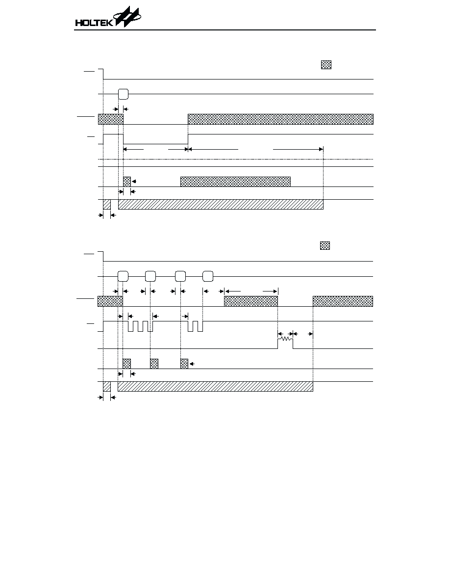
Normal dialing
·
Pulse mode
·
Tone mode
HT9320
21
July 21, 1999
P O
H K S
K E Y I N
T
D B
T
P D P
T
M
T
M
T
B
T
I D P
- T
M
T
P D P
T
I D P
H i g h I m p e d a n c e
X M U T E
R
D 2
D 1
T
D B
T
M
T
I D P
- T
M
T
D B
D T M F
K T
X 2
T
K T
T
K T
T
K T
T
I D P
- T
M
1 . 2 k H z c a r r i e r
2 0 m s
2 0 m s
X 2
D T M F
H i g h I m p e d a n c e
T
D B
T
I T P M
T
I T P M
T
T M I N
K E Y I N
R
D 1
T
I T P M
T
I T P M
K T
T
D B
T
D B
D 2
P O
H K S
X M U T E
2 0 m s
2 0 m s
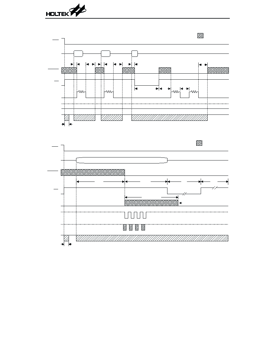
Dialing with Pause key
·
Pulse mode
·
Tone mode
HT9320
22
July 21, 1999
K E Y I N
X 2
T
I D P
T
D B
H i g h I m p e d a n c e
D 3
D 2
D 1
T
I D P
T
M
T
P
+ T
P D P
P
T
I D P
- T
M
D T M F
K T
T
K T
T
K T
T
D B
T
D B
T
D B
1 . 2 k H z c a r r i e r
P O
H K S
X M U T E
T
P D P
2 0 m s
X 2
D T M F
H i g h I m p e d a n c e
T
D B
T
I T P M
K E Y I N
D 3
D 2
T
T M I N
T
I T P M
P
T
P
T
I T P M
D 1
K T
P O
H K S
X M U T E
2 0 m s
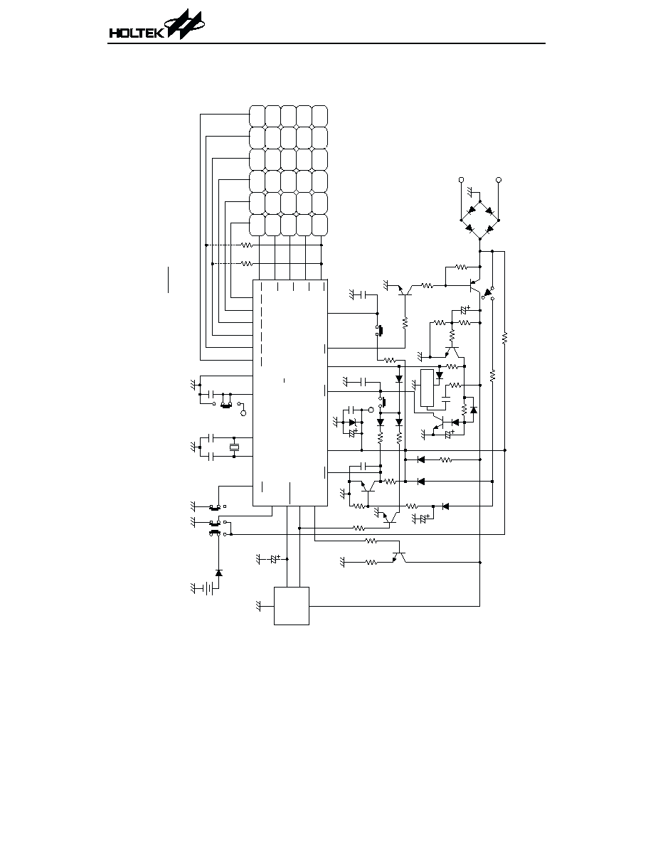
Flash key operation
Pulse ® Tone operation
HT9320
23
July 21, 1999
K E Y I N
X 2
T
F P
T
F
H i g h I m p e d a n c e
T
D B
2 0 m s
D T M F
K T
T
K T
1 . 2 k H z c a r r i e r
P O
H K S
X M U T E
F
K E Y I N
X 2
D T M F
H i g h I m p e d a n c e
T
P D P
T
I D P
+ T
P D P
T
T M I N
T
D B
T
I T P M
T
I D P
T
P
®
T
D 1
2 0 m s
D 2
D 3
* / T
K T
T
D B
T
D B
T
K T
1 . 2 k H z c a r r i e r
P O
H K S
X M U T E
One key redial operation
CLOCK & DOUT operating
HT9320
24
July 21, 1999
T
R P
( 1 s e c )
T
B R K
( 1 . 2 s e c s )
T
I T P M
T
I T P M
H i g h I m p e d a n c e
T
I T P M
T
I T P M
K E Y I N
X 2
D T M F
D 1
D 2
R
K T
T
D B
T
D B
T
D B
P O
H K S
X M U T E
2 0 m s
N o t e : D 1 = D 3 = 3
D 2 = 2
F
C L O C K
= 2 . 4 k H z
D a t a
T
P D P
T
D B
T
B
T
M
H i g h I m p e d a n c e
X 2
D 1
C L O C K
D O U T
K T
T
K T
( 3 4 m s )
1 . 2 k H z C a r r i e r
K E Y I N
P O
H K S
X M U T E
2 0 m s
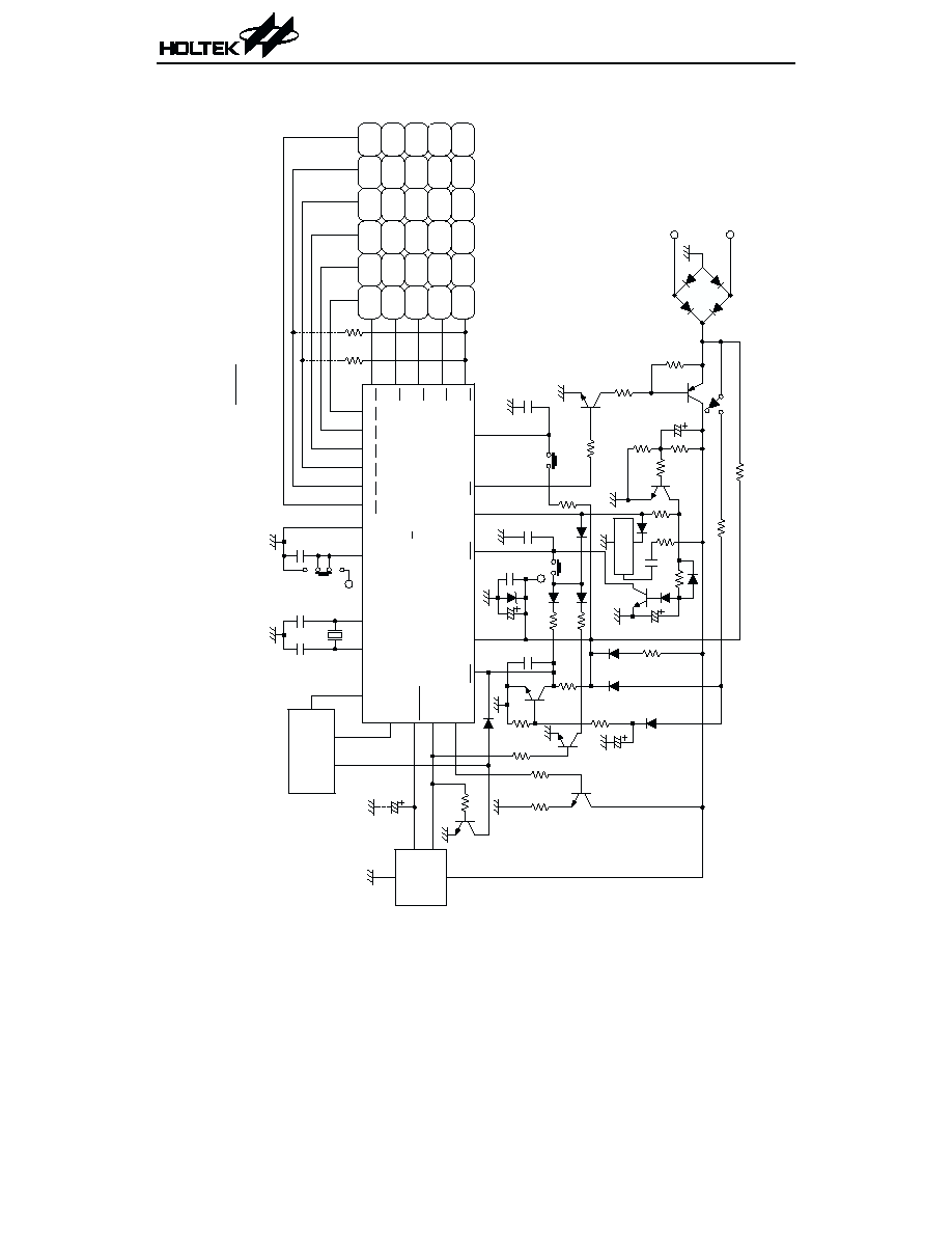
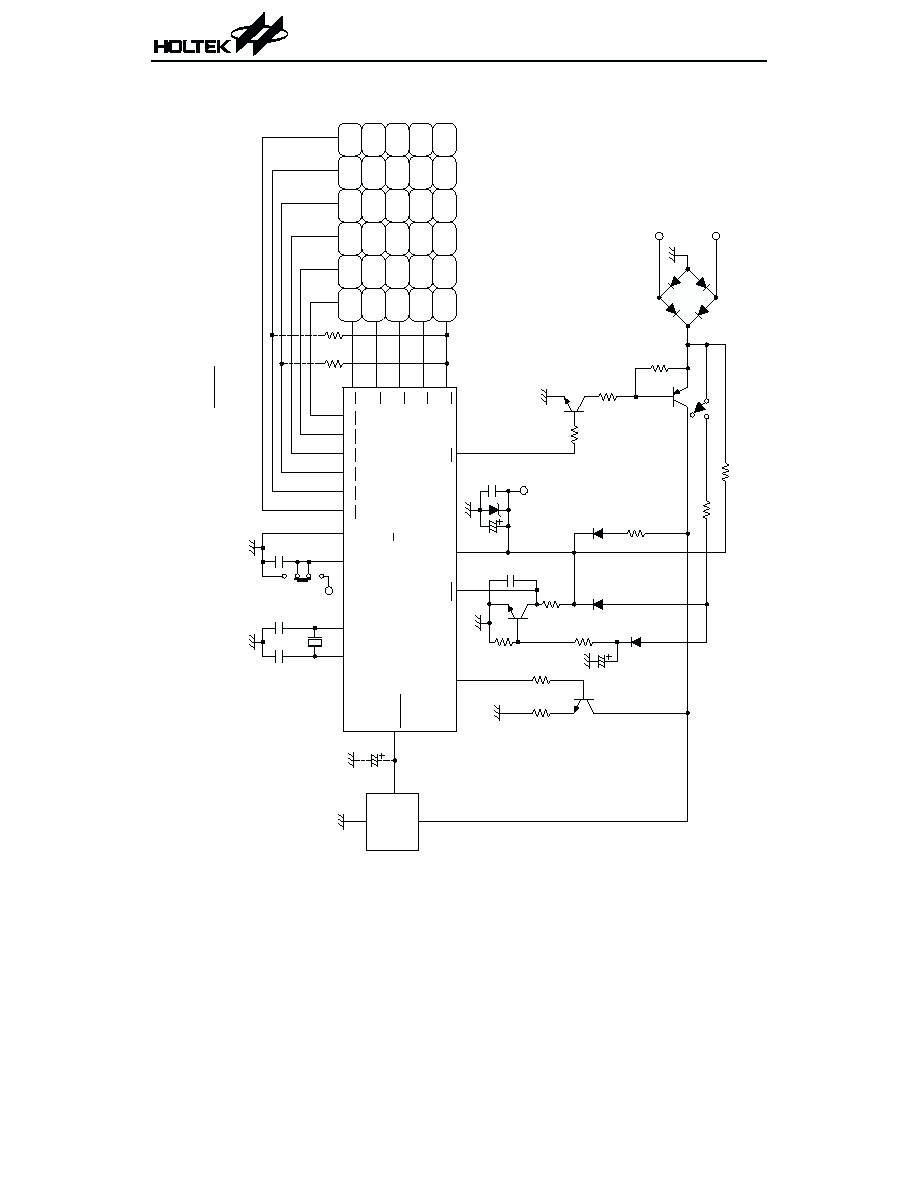
Application Circuits
Application circuit 1
HT9320
25
July 21, 1999
R1
R2
R3
R4
R5
PO
HDI
HK
S
27
26
25
24
23
22
VS
S
M
O
D
E
X
1
X
2
15
11
VD
D
10p
ps
20pp
s
To
n
e
12
13
3.
58
M
H
z
r
e
s
onat
or
VD
D
HF
I
H
DO
150
W
8
14
5.
1
V
Ho
l
d
1N
4148
1N
4148
1N
4148
17
16
21
10
1N
4148
x
4
1
m
F
16V
1N
4148
H
andf
r
e
e
A4
2
10
m
F
50V
A9
2
22M
W
Ti
p
Ri
n
g
1A
b
r
i
d
g
e
Rk
Rk
P
2
5
8
0
SA
1
4
7
*/
T
3
6
9
#
F
A
ST
R
PA
G
E
H
T
38
1X
X
10pF
3
4
5
6
7
C6
C5
C4
C3
C2
C1
1
m
F
DT
M
F
HF
O
*
R
k
i
s
f
o
r
t
he
di
al
i
n
g
s
i
gnal
opt
i
o
n
(
R
e
f
e
r
to
th
e
fu
n
c
ti
o
n
a
l
d
e
s
c
r
i
p
ti
o
n
)
*
U
n
s
p
ec
i
f
i
ed
t
r
ans
i
s
t
o
r
s
a
r
e
o
f
8050
t
ype
*
A
1
m
F
c
apac
i
t
or
b
et
w
e
en
X
M
U
T
E
a
nd
V
S
S
(
G
N
D
)
i
s
r
e
c
o
m
m
ended
*
T
h
e
H
T
381X
X
(
H
T
3810
s
e
r
i
es
)
pr
ov
i
des
a
m
el
ody
dur
i
n
g
t
h
e
hol
d
per
i
o
d
9
2
HS
T
1N
4148
3~
5V
33/
6
6
40/
6
0
O
n
-
hook
st
o
r
e
O
f
f
-
hoo
k
st
o
r
e
M6
/
M7
/
M8
/
M9
/
M
10/
M1
6
M1
7
M1
8
M1
9
M2
0
M1
/
M2
/
M3
/
M4
/
M5
/
M1
1
M1
2
M1
3
M1
4
M1
5
18
20
19
M/
B
XM
U
T
E
SP
EE
C
H
NE
T
W
O
R
K
VD
D
39pF
39pF
1
m
F
1.
5k
W
47k
W
100k
W
270k
W
220k
W
0.
1
m
F
100
m
F
2.
2k
W
22k
W
22k
W
100k
W
220k
W
0.
1
m
F
1
m
F
0.
1
m
F
330k
W
4.
7k
W
220k
W
33k
W
10k
W
47k
W
100k
W
0.
02
m
F
3.
3k
W
100k
W
O
f
f
-
hoo
k
O
n
-
hook
H
T
9320A
28
D
I
P
Application circuit 2
HT9320
26
July 21, 1999
XM
U
T
E
R1
R2
R3
R4
R5
PO
HDI
HK
S
27
26
25
24
23
22
VS
S
M
O
D
E
X
1
X
2
C
L
O
C
K
15
11
VD
D
10p
ps
20pp
s
To
n
e
12
13
3.
58
M
H
z
r
e
s
onat
or
9
2
VD
D
HF
I
HDO
150
W
8
14
5.
1
V
Ho
l
d
1N
4148
1N
4148
1N
4148
17
16
21
10
1N
4148
x
4
1
m
F
16V
1N
4148
H
andf
r
e
e
A4
2
10
m
F
50V
A9
2
22M
W
Ti
p
Ri
n
g
1A
b
r
i
d
g
e
Rk
Rk
P
2
5
8
0
SA
1
4
7
*/
T
3
6
9
#
F
A
ST
R
PA
G
E
H
T
38
1X
X
10pF
HT
1
6
X
X
L
CD
DRI
V
E
R
(
s
ee
H
T
16X
X
dat
a)
3
4
5
6
7
1N
4148
C6
C5
C4
C3
C2
C1
DT
M
F
HF
O
DO
UT
*
R
k
i
s
f
o
r
t
he
di
al
i
n
g
s
i
gnal
opt
i
o
n
(
R
e
f
e
r
to
th
e
fu
n
c
ti
o
n
a
l
d
e
s
c
r
i
p
ti
o
n
)
*
U
n
s
p
ec
i
f
i
ed
t
r
ans
i
s
t
o
r
s
a
r
e
o
f
8050
t
ype
*
A
1
m
F
c
apac
i
t
or
b
et
w
e
en
X
M
U
T
E
a
nd
V
S
S
(
G
N
D
)
i
s
r
e
c
o
m
m
ended
*
T
h
e
H
T
381X
X
(
H
T
3810
s
e
r
i
es
)
pr
ov
i
des
a
m
el
ody
dur
i
n
g
t
h
e
hol
d
per
i
o
d
M6
/
M7
/
M8
/
M9
/
M
10/
M1
6
M1
7
M1
8
M1
9
M2
0
M1
/
M2
/
M3
/
M4
/
M5
/
M1
1
M1
2
M1
3
M1
4
M1
5
SP
EE
C
H
NE
T
W
O
R
K
18
20
19
VD
D
1
m
F
39pF
39pF
1
m
F
47k
W
47k
W
1.
5k
W
100k
W
270k
W
220k
W
0.
1
m
F
100
m
F
2.
2k
W
22k
W
22k
W
0.
1
m
F
1
m
F
100k
W
220k
W
0.
1
m
F
10k
W
220k
W
4.
7k
W 330k
W
33k
W
100k
W
47k
W
0.
02
m
F
3.
3k
W
100k
W
O
f
f
-
hoo
k
O
n
-
hook
H
T
9320B
/
L
28
D
I
P
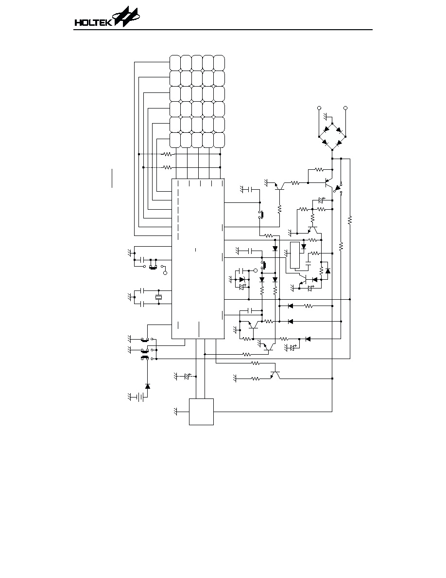
Application circuit 3
HT9320
27
July 21, 1999
XM
U
T
E
R1
R2
R3
R4
R5
PO
HK
S
21
20
19
18
17
16
VS
S
M
O
D
E
X
1
X
2
12
8
VD
D
10p
ps
20pp
s
To
n
e
91
0
3.
58
M
H
z
r
e
s
onat
or
VD
D
150
W
7
11
5.
1
V
1N
4148
1N
4148
15
A4
2
A9
2
22M
W
Ti
p
Ri
n
g
1A
b
r
i
d
g
e
Rk
Rk
P
2
5
8
0
SA
1
4
7
*/
T
3
6
9
#
F
A
ST
R
PA
G
E
10pF
2
3
4
5
6
C6
C5
C4
C3
C2
C1
DT
M
F
*
R
k
i
s
f
o
r
t
he
di
al
i
n
g
s
i
gnal
opt
i
o
n
(
R
e
f
e
r
to
th
e
fu
n
c
ti
o
n
a
l
d
e
s
c
r
i
p
ti
o
n
)
*
U
n
s
p
ec
i
f
i
ed
t
r
ans
i
s
t
o
r
s
a
r
e
o
f
8050
t
ype
*
A
1
m
F
c
apac
i
t
or
b
et
w
e
en
X
M
U
T
E
a
nd
V
S
S
(
G
N
D
)
i
s
r
e
c
o
m
m
ended
M6
/
M7
/
M8
/
M9
/
M
10/
M1
6
M1
7
M1
8
M1
9
M2
0
M1
/
M2
/
M3
/
M4
/
M5
/
M1
1
M1
2
M1
3
M1
4
M1
5
SP
EE
C
H
NE
T
W
O
R
K
13
14
VD
D
1N
4148
1
m
F
39pF
39pF
1
m
F
1.
5k
W
100k
W
220k
W
270k
W
0.
1
m
F
100k
W
2.
2k
W
0.
1
m
F
100
m
F
100k
W
3.
3k
W
47k
W
O
f
f
-
hoo
k
O
n
-
hook
H
T
9320C
22
S
K
D
I
P
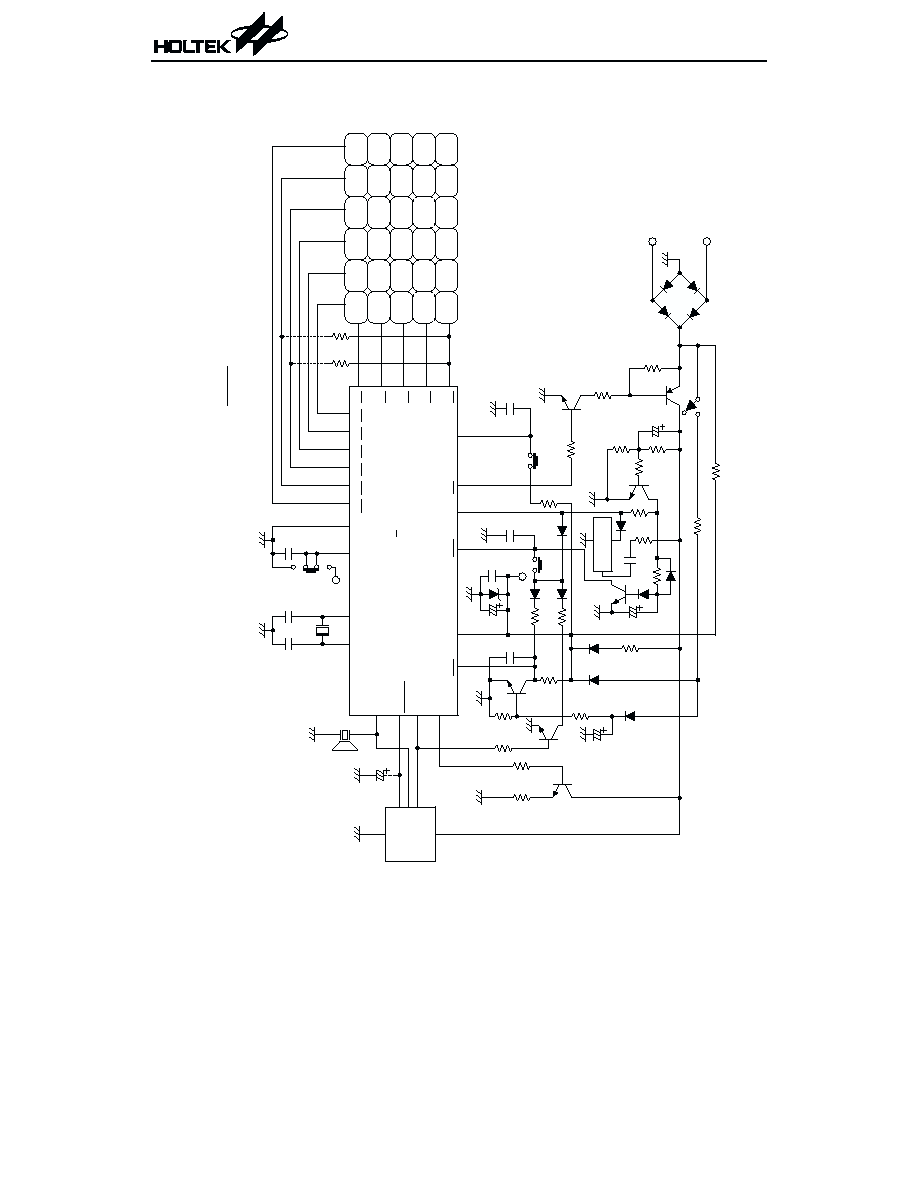
Application circuit 4
HT9320
28
July 21, 1999
XM
U
T
E
R1
R2
R3
R4
R5
PO
HDI
HK
S
27
26
25
24
23
22
VS
S
M
O
D
E
X
1
X
2
15
11
VD
D
10p
ps
20pp
s
To
n
e
12
13
3.
58
M
H
z
r
e
s
onat
or
9
2
VD
D
HF
I
H
DO
150
W
8
14
5.
1
V
Ho
l
d
1N
4148
1N
4148
1N
4148
17
16
21
10
1N
4148
x
4
1
m
F
16V
1N
4148
H
andf
r
e
e
A4
2
10
m
F
50V
A9
2
22M
W
Ti
p
Ri
n
g
1A
b
r
i
d
g
e
Rk
Rk
2
5
8
0
SA
1
4
7
*
3
6
9
#
P
®
T
F
A
ST
R/
P
PA
G
E
H
T
38
1X
X
10pF
3
4
5
6
7
H
ook
o
f
f
H
ook
o
n
C6
C5
C4
C3
C2
C1
DT
M
F
HF
O
HS
T
*
R
k
i
s
f
o
r
t
he
di
al
i
n
g
s
i
gnal
opt
i
o
n
(
R
e
f
e
r
to
th
e
fu
n
c
ti
o
n
a
l
d
e
s
c
r
i
p
ti
o
n
)
*
U
n
s
p
ec
i
f
i
ed
t
r
ans
i
s
t
o
r
s
a
r
e
o
f
8050
t
ype
*
A
1
m
F
c
apac
i
t
or
b
et
w
e
en
X
M
U
T
E
a
nd
V
S
S
(
G
N
D
)
i
s
r
e
c
o
m
m
ended
*
T
h
e
H
T
381X
X
(
H
T
3810
s
e
r
i
es
)
pr
ov
i
des
a
m
el
ody
dur
i
n
g
t
h
e
hol
d
per
i
o
d
1N
4148
3~
5V
40/
60
33/
66
O
n
-
hook
st
o
r
e
O
f
f
-
hoo
k
st
o
r
e
M/
B
18
20
19
SP
EE
C
H
NE
T
W
O
R
K
VD
D
M6
/
M7
/
M8
/
M9
/
M
10/
M1
6
M1
7
M1
8
M1
9
M2
0
M1
/
M2
/
M3
/
M4
/
M5
/
M1
1
M1
2
M1
3
M1
4
M1
5
1
m
F
39pF
39pF
1
m
F
1.
5k
W
47k
W
100k
W
270k
W
220k
W
2.
2k
W
0.
1
m
F
100
m
F
22k
W
22k
W
0.
1
m
F
1
m
F
10k
W
0.
1
m
F
100k
W
220k
W
4.
7k
W 330k
W
220k
W
100k
W
33k
W
47k
W
100k
W
0.
02
m
F
3.
3k
W
H
T
9320H
28
D
I
P
Application circuit 5
HT9320
29
July 21, 1999
XM
U
T
E
R1
R2
R3
R4
R5
PO
HDI
HK
S
27
26
25
24
23
22
VS
S
M
O
D
E
X
1
X
2
15
11
VD
D
10p
ps
20pp
s
To
n
e
12
13
3.
58
M
H
z
r
e
s
onat
or
2
VD
D
HF
I
HDO
150
W
8
14
5.
1
V
Ho
l
d
1N
4148
1N
4148
1N
4148
17
16
21
10
1N
4148
x
4
1
m
F
16V
1N
4148
H
andf
r
e
e
A4
2
10
m
F
50V
A9
2
22M
W
Ti
p
Ri
n
g
1A
b
r
i
d
g
e
Rk
Rk
P
2
5
8
0
SA
1
4
7
*/
T
3
6
9
#
F
A
ST
R
PA
G
E
H
T
38
1X
X
10pF
3
4
5
6
7
C6
C5
C4
C3
C2
C1
DT
M
F
HF
O
KT
*
R
k
i
s
f
o
r
t
he
di
al
i
n
g
s
i
gnal
opt
i
o
n
(
R
e
f
e
r
to
th
e
fu
n
c
ti
o
n
a
l
d
e
s
c
r
i
p
ti
o
n
)
*
U
n
s
p
ec
i
f
i
ed
t
r
ans
i
s
t
o
r
s
a
r
e
o
f
8050
t
ype
*
A
1
m
F
c
apac
i
t
or
b
et
w
e
en
X
M
U
T
E
a
nd
V
S
S
(
G
N
D
)
i
s
r
e
c
o
m
m
ended
*
T
h
e
H
T
381X
X
(
H
T
3810
s
e
r
i
es
)
pr
ov
i
des
a
m
el
ody
dur
i
n
g
t
h
e
hol
d
per
i
o
d
B
u
zze
r
SP
EE
C
H
NE
T
W
O
R
K
VD
D
M6
/
M7
/
M8
/
M9
/
M
10/
M1
6
M1
7
M1
8
M1
9
M2
0
M1
/
M2
/
M3
/
M4
/
M5
/
M1
1
M1
2
M1
3
M1
4
M1
5
18
20
19
1
m
F
39pF
39pF
1
m
F
0.
1
m
F
100
m
F
1.
5k
W
47k
W
100k
W
270k
W
220k
W
2.
2k
W
22k
W
22k
W
0.
1
m
F
100k
W
220k
W
1m
F
0.
1m
F
330k
W
10k
W
4.
7k
W
220k
W
100k
W
47k
W
33k
W
0.
02
m
F
100k
W
3.
3k
W
O
f
f
-
hoo
k
O
n
-
hook
H
T
9320K
28
D
I
P

HT9320
30
July 21, 1999
Copyright ã 1999 by HOLTEK SEMICONDUCTOR INC.
The information appearing in this Data Sheet is believed to be accurate at the time of publication. However, Holtek
assumes no responsibility arising from the use of the specifications described. The applications mentioned herein are
used solely for the purpose of illustration and Holtek makes no warranty or representation that such applications
will be suitable without further modification, nor recommends the use of its products for application that may pres-
ent a risk to human life due to malfunction or otherwise. Holtek reserves the right to alter its products without prior
notification. For the most up-to-date information, please visit our web site at http://www.holtek.com.tw.
Holtek Semiconductor Inc. (Headquarters)
No.3 Creation Rd. II, Science-based Industrial Park, Hsinchu, Taiwan, R.O.C.
Tel: 886-3-563-1999
Fax: 886-3-563-1189
Holtek Semiconductor Inc. (Taipei Office)
5F, No.576, Sec.7 Chung Hsiao E. Rd., Taipei, Taiwan, R.O.C.
Tel: 886-2-2782-9635
Fax: 886-2-2782-9636
Fax: 886-2-2782-7128 (International sales hotline)
Holtek Microelectronics Enterprises Ltd.
RM.711, Tower 2, Cheung Sha Wan Plaza, 833 Cheung Sha Wan Rd., Kowloon, Hong Kong
Tel: 852-2-745-8288
Fax: 852-2-742-8657
Document Outline
- þÿ
- þÿ
- þÿ
- þÿ
- þÿ
- þÿ
- þÿ
- þÿ
- þÿ
- þÿ
- þÿ
- þÿ
- þÿ
- þÿ