Document Outline
- ■
- ■
- ■
- ■
- ■
- ■
- ■
- ■
- ■
- ■
- ■
- ■
- ■
- ■
- ■

HT36A0
8-Bit Music Synthesizer MCU
Block Diagram
Rev. 1.20
1
June 18, 2003
Features
À
Operating voltage: 3.6V~5.0V
À
Operating frequency: 3.58MHz~12MHz
(typ. 11.059MHz)
À
28 bidirectional I/O lines
À
Two 16-bit programmable timer/event counters with
overflow interrupts
À
Watchdog Timer
À
Built-in 8-bit MCU with 208
┤8 bits RAM
À
Built-in 64K
┤16-bit ROM for program/data shared
À
Digital output pins for external DAC
À
Single data format with 16 bits digital stereo audio
output
À
Two High D/A converter resolution: 16 bits
À
Polyphonic up to 16 notes
À
Independent pan and volume mix can be assigned to
each sound component
À
Sampling rate of 44.1kHz as 11.059MHz for system
frequency
À
Eight-level subroutine nesting
À
HALT function and wake-up feature to reduce power
consumption
À
Bit manipulation instructions
À
16-bit table read instructions
À
63 powerful instructions
À
All instructions in 1 or 2 machine cycles
À
48-pin SSOP package
General Description
The HT36A0 is an 8-bit high performance RISC-like
microcontroller specifically designed for music applica-
tions. It provides an 8-bit MCU and a 16 channel
wavetable synthesizer. The program ROM is composed
of both program control codes and wavetable voice
codes, and can be easily programmed.
The HT36A0 has a built-in 8-bit microprocessor which
programs the synthesizer to generate the melody by
setting the special register from 20H~2AH. A HALT fea-
ture is provided to reduce power consumption.
8 - B i t
M C U
6 4 K ┤ 1 6 - b i t
R O M
2 0 8 ┤ 8
R A M
M u l t i p l i e r / P h a s e
G e n e r a l
1 6 - B i t
D A C
P A 0 ~ P A 7
P B 0 ~ P B 7
P C 0 ~ P C 7
P D 0 ~ P D 3
O S C 1
O S C 2
R E S
1 6 - B i t
D A C
V D D
V S S
V D D A
R C H
L C H
P
D
3
/
D
C
L
K
P
D
2
/
L
O
A
D
P
D
1
/
D
O
U
T
P F 0 ~ 2
V S S A

Pin Assignment
Pad Assignment
Chip size: 120.5
┤ 124.4 (mil)
* The IC substrate should be connected to VSS in the PCB layout artwork.
HT36A0
Rev. 1.20
2
June 18, 2003
4 8
4 7
4 6
4 5
4 4
4 3
4 2
4 1
4 0
3 9
3 8
3 7
3 6
3 5
3 4
3 3
3 2
3 1
3 0
2 9
2 8
2 7
2 6
2 5
1
2
3
4
5
6
7
8
9
1 0
1 1
1 2
1 3
1 4
1 5
1 6
1 7
1 8
1 9
2 0
2 1
2 2
2 3
2 4
N C
O S C 1
V S S
V S S
V D D
N C
N C
P A 0
P A 1
P A 2
P A 3
P A 4
P A 5
P A 6
P A 7
P B 0
P B 1
N C
P B 2
P B 3
P B 4
P B 5
P B 6
N C
N C
O S C 2
V D D A
L C H
R C H
V S S A
N C
R E S
P D 3
P D 2
P D 1
P D 0
P C 7
P C 6
P C 5
P C 4
N C
N C
P C 3
P C 2
P C 1
P C 0
P B 7
N C
H T 3 6 A 0
4 8 S S O P - A
3 8 3 7 3 6
3 5
( 0 , 0 )
3 4 3 3
3 2
3 1
3 0
2 9
2 8
2 7
2 6
2 5
2 4
2 3
2 2
2 1
2 0
1 9
1 8
1 7
1 6
1 5
1 4
1 3
1 2
1 1
1 0
9
8
7
6
5
4
3
2
1
P A 0
P A 1
P A 2
P A 3
P A 4
P A 5
P A 6
P A 7
P B 0
P B 1
P
B
2
P
B
3
P
B
4
P
B
5
P
B
6
P
B
7
P
C
0
P
C
1
P
C
2
P
C
3
P C 4
P C 5
P C 6
P C 7
R E S
P D 3
P D 2
P D 1
P D 0
R
C
H
L
C
H
O
S
C
2
O
S
C
1
V
S
S
V
S
S
V
D
D
V
D
D
A
V
S
S
A

Pad Coordinates
Unit:
mm
Pad No.
X
Y
Pad No.
X
Y
1
-1365.58
1008.20
20
1273.90
-1415.28
2
-1365.58
748.60
21
1367.30
-1106.75
3
-1365.58
489.00
22
1367.30
-847.15
4
-1365.58
229.40
23
1367.30
-587.55
5
-1365.58
-30.2
24
1367.30
-327.95
6
-1365.58
-289.80
25
1367.30
-68.35
7
-1365.58
-549.40
26
1367.30
191.25
8
-1365.58
-809.00
27
1367.30
450.85
9
-1365.58
-1068.60
28
1367.30
710.45
10
-1365.58
-1328.20
29
1367.30
970.05
11
-1062.50
-1415.28
30
1172.575
1414.78
12
-802.90
-1415.28
31
965.075
1414.78
13
-543.30
-1415.28
32
705.475
1414.78
14
-283.70
-1415.28
33
497.925
1414.78
15
-24.10
-1415.28
34
349.436
1396.935
16
235.50
-1415.28
35
-328.416
1396.935
17
495.10
-1415.28
36
-481.370
1368.13
18
754.70
-1415.28
37
-611.375
1368.13
19
1014.30
-1415.28
38
-741.385
1368.13
Pad Description
Pad No.
Pad Name
I/O
Internal
Connection
Function
1~8
PA0~PA7
I/O
Pull-High
or None
Bidirectional 8-bit Input/Output port, wake-up by mask option
9~16
PB0~PB7
I/O
Pull-High
or None
Bidirectional 8-bit Input/Output port
17~24
PC0~PC7
I/O
Pull-High
or None
Bidirectional 8-bit Input/Output port
25
PD0
I/O
Pull-High
or None
Bidirectional 8-bit Input/Output port
26
PD1/DOUT
I/O
Pull-High
or None
Bidirectional 8-bit Input/Output port DAC data out
27
PD2/LOAD
I/O
Pull-High
or None
Bidirectional 8-bit Input/Output port DAC word clock
28
PD3/DCLK
I/O
Pull-High
or None
Bidirectional 8-bit Input/Output port DAC bit clock
29
RES
I
¥
Reset input, active low
30
VSSA
¥
¥
Negative power supply of DAC, ground
31
RCH
O
CMOS
R channel audio output
32
LCH
O
CMOS
L channel audio output
33
VDDA
¥
¥
DAC power supply
35
34
OSC1
OSC2
I
O
¥
OSC1 and OSC2 are connected to an RC network or a crystal (by
mask option) for the internal system clock. In the case of RC opera-
tion, OSC2 is the output terminal for 1/8 system clock. The system
clock may come from the crystal, the two pins cannot be floating.
36, 37
VSS
¥
¥
Negative power supply, ground
38
VDD
¥
¥
Positive power supply
HT36A0
Rev. 1.20
3
June 18, 2003

Absolute Maximum Ratings
Supply Voltage ...........................................
-0.3V to 6V
Storage Temperature ...........................
-50░C to 125░C
Input Voltage .............................V
SS
-0
.
3V to V
DD
+0.3V
Operating Temperature ..........................
-25░C to 70░C
Note: These are stress ratings only. Stresses exceeding the range specified under
▓Absolute Maximum Ratings▓ may
cause substantial damage to the device. Functional operation of this device at other conditions beyond those
listed in the specification is not implied and prolonged exposure to extreme conditions may affect device reliabil-
ity.
D.C. Characteristics
Ta=25
░C
Symbol
Parameter
Test Conditions
Min.
Typ.
Max.
Unit
V
DD
Conditions
V
DD
Operating Voltage
¥
¥
3.6
5
6
V
I
DD
Operating Current
5V
No load
f
OSC
=11.0592MHz
¥
8
16
mA
I
STB
Standby Current (WDT Disabled)
5V
No load
System HALT
¥
0
¥
mA
I
OL
I/O Ports Sink Current
5V
V
OL
=0.5V
9.7
16.2
¥
mA
I
OH
I/O Ports Source Current
5V
V
OH
=4.5V
-5.2
-8.7
¥
mA
R
PH
Pull-High Resistance of I/O Ports
5V
V
IL
=0V
11
22
44
k
W
V
IH1
Input High Voltage for I/O Ports
5V
¥
3.5
¥
5
V
V
IL1
Input Low Voltage for I/O Ports
5V
¥
0
¥
1.5
V
V
IH2
Input High Voltage (RES)
5V
¥
¥
4
¥
V
V
IL2
Input Low Voltage (RES)
5V
¥
¥
2.5
¥
V
A.C. Characteristics
Symbol
Parameter
Test Conditions
Min.
Typ.
Max.
Unit
V
DD
Conditions
MCU interface
f
OSC
System Frequency
5V
12MHz crystal
¥
12
¥
MHz
f
SYS
System Clock
5V
¥
4
¥
16
MHz
t
WDT
Watchdog Time-Out Period (RC)
¥
Without WDT prescaler
9
17
35
ms
t
RES
External Reset Low Pulse Width
¥
¥
1
¥
¥
ms
Symbol
Parameter
Figure
Min.
Typ.
Max.
Unit
DAC interface
f
BC
DCK Bit Clock Frequency
Fig 1
¥
f
SYS
/16
¥
MHz
t
CH
DCK Bit Clock H Level Time
Fig 1
600
¥
¥
ns
t
DOS
Data Output Setup Time
Fig 1
200
¥
¥
ns
t
DOH
Data Output Hold Time
Fig 1
200
¥
¥
ns
t
LCS
Load Clock Setup Time
Fig 1
200
¥
¥
ns
t
LCH
Load Clock Hold Time
Fig 1
200
¥
¥
ns
HT36A0
Rev. 1.20
4
June 18, 2003
Characteristics Curves
V vs F Characteristics Curve
HT36A0
Rev. 1.20
5
June 18, 2003
1 / f
B C
t
C H
V
O H
V
O L
t
D O H
t
D O S
V
O H
V
O L
L S B
V
O H
V
O L
t
L C H
t
L C S
L O A D
I I S
D C K
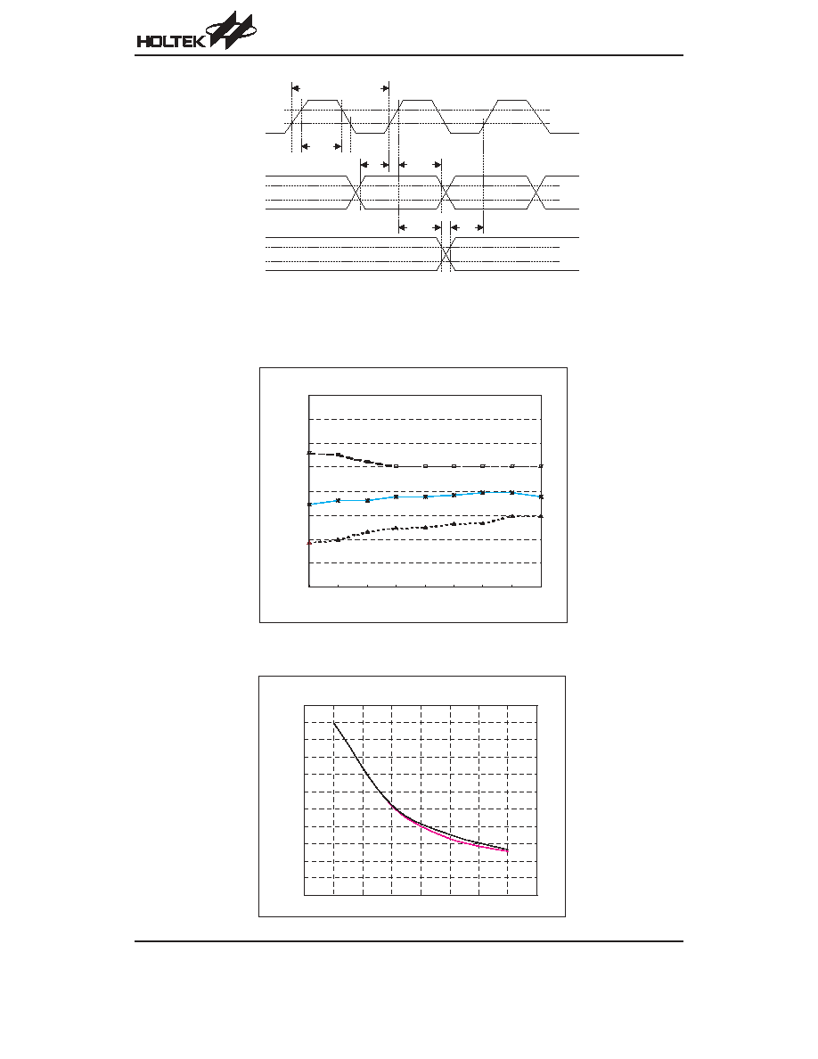
Fig 1. Audio output timing
9 . 0
9 . 5
1 0 . 0
1 0 . 5
1 1 . 0
1 1 . 5
1 2 . 0
1 2 . 5
1 3 . 0
3 . 1
3 . 4
3 . 7
4
4 . 3
4 . 6
4 . 9
5 . 2
5 . 5
V o l t a g e ( V )
F
r
e
q
u
e
n
c
y
(
M
H
z
)
R = 5 1 k W
R = 5 3 k W
H T 3 6 A 0 V v s F C h a r t
R = 4 9 k W
4
5
6
7
8
9
1 0
1 1
1 2
1 3
1 4
1 5
4 3
5 6
6 8
7 5
F
r
e
q
u
e
n
c
y
(
M
H
z
)
V 2 = 4 . 5 V
V 3 = 5 . 0 V
H T 3 6 A 0 R v s F C h a r t
k W

HT36A0
Rev. 1.20
6
June 18, 2003
Function Description
Execution Flow
The system clock for the HT36A0 is derived from either
a crystal or an RC oscillator. The oscillator frequency di-
vided by 2 is the system clock for the MCU and it is inter-
nally divided into four non-overlapping clocks. One
instruction cycle consists of four system clock cycles.
Instruction fetching and execution are pipelined in such
a way that a fetch takes one instruction cycle while de-
coding and execution takes the next instruction cycle.
However, the pipelining scheme causes each instruc-
tion to effectively execute in one cycle. If an instruction
changes the program counter, two cycles are required
to complete the instruction.
Program Counter
- PC
The 13-bit program counter (PC) controls the sequence
in which the instructions stored in program ROM are ex-
ecuted and its contents specify a maximum of 8192 ad-
dresses for each bank.
After accessing a program memory word to fetch an in-
struction code, the contents of the program counter are
incremented by one. The program counter then points
to the memory word containing the next instruction
code.
When executing a jump instruction, conditional skip ex-
ecution, loading PCL register, subroutine call, initial re-
set, internal interrupt, external interrupt or return from
subroutine, the PC manipulates the program transfer by
loading the address corresponding to each instruction.
The conditional skip is activated by instruction. Once the
condition is met, the next instruction, fetched during the
current instruction execution, is discarded and a dummy
cycle replaces it to retrieve the proper instruction. Other-
wise proceed with the next instruction.
The lower byte of the program counter (PCL) is a read-
able and writeable register (06H). Moving data into the
PCL performs a short jump. The destination will be
within 256 locations.
Once a control transfer takes place, an additional
dummy cycle is required.
Program ROM
HT36A0 provides 16 address lines WA[15:0] to read the
Program ROM which is up to 1M bits, and is commonly
used for the wavetable voice codes and the program
memory. It provides two address types, one type is for
program ROM, which is addressed by a bank pointer
PF2~0 and a 13-bit program counter PC 12~0; and the
T 1
T 2
T 3
T 4
T 1
T 2
T 3
T 4
T 1
T 2
T 3
T 4
F e t c h I N S T ( P C )
E x e c u t e I N S T ( P C - 1 )
F e t c h I N S T ( P C + 1 )
E x e c u t e I N S T ( P C )
F e t c h I N S T ( P C + 2 )
E x e c u t e I N S T ( P C + 1 )
P C
P C + 1
P C + 2
S y s t e m C l o c k o f M C U
( S y s t e m C l o c k / 2 )
P C
Execution flow
Mode
Program Counter
*12
*11
*10
*9
*8
*7
*6
*5
*4
*3
*2
*1
*0
Initial Reset
0
0
0
0
0
0
0
0
0
0
0
0
0
Timer/Event Counter 0 Overflow
0
0
0
0
0
0
0
0
0
1
0
0
0
Timer/Event Counter 1 Overflow
0
0
0
0
0
0
0
0
0
1
1
0
0
Skip
PC+2
Loading PCL
*12
*11
*10
*9
*8
@7
@6
@5
@4
@3
@2
@1
@0
Jump, Call Branch
#12
#11
#10
#9
#8
#7
#6
#5
#4
#3
#2
#1
#0
Return From Subroutine
S12
S11
S10
S9
S8
S7
S6
S5
S4
S3
S2
S1
S0
Program counter
Note:
*12~*0: Bits of Program Counter
@7~@0: Bits of PCL
#12~#0: Bits of Instruction Code
S12~S0: Bits of Stack Register
@7~@0: Bits of PCL

HT36A0
Rev. 1.20
7
June 18, 2003
other type is for wavetable code, which is addressed by
the start address ST15~0. On the program type,
WA15~0= PF2~0
┤ 2
13
+ PC12~0. On the wave table
ROM type, WA15~0=ST15~0
┤ 2
5
.
Program Memory
- ROM
The program memory is used to store the program in-
structions which are to be executed. It also contains
data, table, and interrupt entries, and is organized into
8192
┤16 bits, addressed by the bank pointer, program
counter and table pointer.
Certain locations in the program memory of each bank
are reserved for special usage:
À
Location 000H on bank0
This area is reserved for the initialization program. Af-
ter chip reset, the program always begins execution at
location 000H on bank0.
À
Location 008H
This area is reserved for the Timer/Event Counter 0 in-
terrupt service program on each bank. If timer interrupt
results from a timer/event counter 0 overflow, and if the
interrupt is enabled and the stack is not full, the program
begins execution at location 008H corresponding to its
bank.
À
Location 00CH
This area is reserved for the Timer/Event Counter 1
interrupt service program on each bank. If a timer in-
terrupt results from a Timer/Event Counter 1 overflow,
and if the interrupt is enabled and the stack is not full,
the program begins execution at location 00CH corre-
sponding to its bank.
À
Table location
Any location in the ROM space can be used as
look-up tables. The instructions TABRDC [m] (the cur-
rent page, 1 page=256 words) and TABRDL [m] (the
last page) transfer the contents of the lower-order
byte to the specified data memory, and the
higher-order byte to TBLH (08H). Only the destination
of the lower-order byte in the table is well-defined, the
higher-order byte of the table word are transferred to
the TBLH. The Table Higher-order byte register
(TBLH) is read only. The Table Pointer (TBLP) is a
read/write register (07H), which indicates the table lo-
cation. Before accessing the table, the location must
be placed in TBLP. The TBLH is read only and cannot
be restored. If the main routine and the ISR (Interrupt
Service Routine) both employ the table read instruc-
tion, the contents of the TBLH in the main routine are
likely to be changed by the table read instruction used
in the ISR. Errors can occur. In this case, using the ta-
ble read instruction in the main routine and the ISR si-
multaneously should be avoided. However, if the table
read instruction has to be applied in both the main rou-
tine and the ISR, the interrupt should be disabled prior
to the table read instruction. It will not be enabled until
the TBLH has been backed up. All table related in-
structions need 2 cycles to complete the operation.
These areas may function as normal program mem-
ory depending upon user requirements.
À
Bank pointer
The program memory is organized into 8 banks and
each bank into 8192
┤ 16 of bits program ROM.
PF[2~0] is used as the bank pointer only when PFC is
configured as output mode. PFC is the control register
for PF and is used to control the input/output configu-
ration. To function as an output, the corresponding bit
of the control register must be
▓0▓. After an instruction
has been executed to write data to the PF register to
select a different bank, note that the new bank will not
be selected immediately. It is not until the following in-
struction has completed execution that the bank will
be actually selected. It should be note that the PF reg-
ister has to be cleared before setting to output mode.
0 0 0 0 H
0 0 0 8 H
T i m e r / e v e n t C o u n t e r 0 i n t e r r u p t s u b r o u t i n e
P r o g r a m
R O M
1 6 b i t s
L o o k - u p t a b l e ( 2 5 6 w o r d s )
n 0 0 H
L o o k - u p t a b l e ( 2 5 6 w o r d s )
1 F F F H
N o t e : n r a n g e s f r o m 0 0 t o 1 F .
n F F H
T i m e r / e v e n t C o u n t e r 1 i n t e r r u p t s u b r o u t i n e
0 0 0 C H
D e v i c e i n i t i a l i z a t i o n p r o g r a m
Program memory for each bank
Instruction(s)
Table Location
*12
*11
*10
*9
*8
*7
*6
*5
*4
*3
*2
*1
*0
TABRDC [m]
P12
P11
P10
P9
P8
@7
@6
@5
@4
@3
@2
@1
@0
TABRDL [m]
1
1
1
1
1
@7
@6
@5
@4
@3
@2
@1
@0
Table location
Note:
*12~*0: Bits of table location
@7~@0: Bits of table pointer
P12~P8: Bits of current Program Counter

HT36A0
Rev. 1.20
8
June 18, 2003
Wavetable ROM
The ST[15~0] is used to defined the start address of
each sample on the wavetable and read the waveform
data from the location. HT36A0 provides 21 output ad-
dress lines from WA[16~0], the ST[15~0] is used to lo-
cate the major 16 bits i.e. WA[16:5] and the undefined
data from WA[4~0] is always set to 00000b. So the start
address of each sample have to be located at a multiple
of 32. Otherwise, the sample will not be read out cor-
rectly because it has a wrong starting code.
Stack Register
- Stack
This is a special part of the memory which is used to
save the contents of the program counter (PC) only. The
stack is organized into 8 levels and is neither part of the
data nor part of the program space, and is neither read-
able nor writeable. The activated level is indexed by the
stack pointer (SP) and is neither readable nor writeable.
At a subroutine call or interrupt acknowledgment, the
contents of the program counter are pushed onto the
stack. At the end of a subroutine or an interrupt routine,
signaled by a return instruction (RET or RETI), the pro-
gram counter is restored to its previous value from the
stack. After a chip reset, the SP will point to the top of the
stack.
If the stack is full and a non-masked interrupt takes
place, the interrupt request flag will be recorded but the
acknowledgment will be inhibited. When the stack
pointer is decremented (by RET or RETI), the interrupt
will be serviced. This feature prevents stack overflow al-
lowing the programmer to use the structure more easily.
In a similar case, if the stack is full and a CALL is subse-
quently executed, a stack overflow occurs and the first
entry will be lost (only the most recent eight return ad-
dress are stored).
Data Memory
- RAM
The data memory is designed with 256
┤ 8 bits. The data
memory is divided into three functional groups: special
function registers, wavetable function register, and gen-
eral purpose data memory (208
┤8). Most of them are
read/write, but some are read only.
The special function registers include the Indirect Ad-
dressing register 0 (00H), the Memory Pointer register 0
(MP0;01H), the Indirect Addressing register 1 (02H), the
Memory Pointer register 1 (MP1;03H), the Accumulator
(ACC;05H), the Program Counter Lower-byte register
(PCL;06H), the Table Pointer (TBLP;07H), the Table
Higher-order byte register (TBLH;08H), the Watchdog
Timer option Setting register (WDTS;09H), the Status
register (STATUS;0AH), the Interrupt Control register
(INTC;0BH), the Timer/event Counter 0 Higher-order
byte register (TMR0H;0CH), the Timer/event Counter 0
L o w e r - o r d e r b y t e r e g i s t e r ( T M R 0 L ; 0 D H ) , t h e
Timer/event Counter 0 Control register (TMR0C;0EH),
the Timer/ event Counter 1 Higher-order byte register
(TMR1H;0FH), the Timer/event Counter 1 Lower-order
byte register (TMR1L;10H), the Timer/event Counter 1
Control register (TMR1C;11H), the I/O registers
(PA;12H, PB;14H, PC;16H, PD;18H), the program ROM
bank select (PF;1CH)) and the I/O Control registers
(PAC;13H, PBC;15H, PCC;17H, PDC;19H), and the
S p e c i a l P u r p o s e
D A T A M E M O R Y
0 0 H
0 1 H
0 2 H
0 3 H
0 4 H
0 5 H
0 6 H
0 7 H
0 8 H
0 9 H
0 A H
0 B H
0 C H
0 D H
0 E H
0 F H
1 0 H
1 1 H
1 2 H
1 3 H
1 4 H
1 5 H
1 6 H
1 7 H
1 8 H
1 9 H
1 A H
1 B H
1 C H
1 D H
1 E H
1 F H
2 0 H
2 1 H
2 2 H
2 3 H
2 4 H
2 5 H
2 6 H
2 7 H
2 9 H
2 A H
2 B H
2 F H
G e n e r a l P u r p o s e
D A T A M E M O R Y
( 2 0 8 B y t e s )
F F H
: U n u s e d .
R e a d a s " 0 0 "
I n d i r e c t A d d r e s s i n g R e g i s t e r 0
M P 0
I n d i r e c t A d d r e s s i n g R e g i s t e r 1
M P 1
A C C
P C L
T B L P
T B L H
W D T S
S T A T U S
I N T C
T M R 0 H
T M R 0 L
T M R 0 C
T M R 1 H
T M R 1 L
T M R 1 C
P A
P A C
P B
P B C
P C
P C C
P D
P D C
P F
P F C
C h a n n e l n u m b e r s e l e c t
F r e q u e n c y n u m b e r h i g h b y t e
F r e q u e n c y n u m b e r l o w b y t e
S t a r t a d d r e s s h i g h b y t e
S t a r t a d d r e s s l o w b y t e
R e p e a t n u m b e r h i g h b y t e
R e p e a t n u m b e r l o w b y t e
C o n t r o l r e g i s t e r
L e f t v o l u m n c o n t r o l
R i g h t v o l u m c o n t r o l
2 8 H
3 0 H
W a v e t a b l e F u n c t i o n
R e g i s t e r
RAM mapping

HT36A0
Rev. 1.20
9
June 18, 2003
program ROM bank control register (PFC;1DH). The
wavetable function registers is defined between
20H~2AH. The remaining space before the 30H is re-
served for future expanded usage and reading these lo-
cations will return the result 00H. The general purpose
data memory, addressed from 30H to FFH, is used for
data and control information under instruction command.
All data memory areas can handle arithmetic, logic, in-
crement, decrement and rotate operations directly. Ex-
cept for some dedicated bits, each bit in the data
memory can be set and reset by the SET [m].i and CLR
[m].i instructions, respectively. They are also indirectly
accessible through Memory pointer registers
(MP0;01H, MP1;03H).
Indirect Addressing Register
Location 00H and 02H are indirect addressing registers
that are not physically implemented. Any read/write op-
eration of [00H] and [02H] access data memory pointed
to by MP0 (01H) and MP1 (03H) respectively. Reading
location 00H or 02H directly will return the result 00H.
And writing directly results in no operation.
The function of data movement between two indirect ad-
dressing registers, is not supported. The memory
pointer registers, MP0 and MP1, are 8-bit register which
can be used to access the data memory by combining
corresponding indirect addressing registers.
Accumulator
The accumulator closely relates to ALU operations. It is
mapped to location 05H of the data memory and it can
operate with immediate data. The data movement be-
tween two data memory locations must pass through
the accumulator.
Arithmetic and Logic Unit
- ALU
This circuit performs 8-bit arithmetic and logic operation.
The ALU provides the following functions:
À
Arithmetic operations (ADD, ADC, SUB, SBC, DAA)
À
Logic operations (AND, OR, XOR, CPL)
À
Rotation (RL, RR, RLC, RRC)
À
Increment & Decrement (INC, DEC)
À
Branch decision (SZ, SNZ, SIZ, SDZ ....)
The ALU not only saves the results of a data operation but
can also change the status register.
Status Register
- STATUS
This 8-bit register (0AH) contains the zero flag (Z), carry
flag (C), auxiliary carry flag (AC), overflow flag (OV),
power down flag (PD) and Watchdog time-out flag (TO).
It also records the status information and controls the oper-
ation sequence.
With the exception of the TO and PD flags, bits in the
status register can be altered by instructions like any
other register. Any data written into the status register
will not change the TO or PD flags. In addition it should
be noted that operations related to the status register
may give different results from those intended. The TO
and PD flags can only be changed by system power up,
Watchdog Timer overflow, executing the HALT instruc-
tion and clearing the Watchdog Timer.
The Z, OV, AC and C flags generally reflect the status of
the latest operations.
In addition, on entering the interrupt sequence or exe-
cuting a subroutine call, the status register will not be
automatically pushed onto the stack. If the contents of
status are important and the subroutine can corrupt the
status register, the programmer must take precautions
to save it properly.
Interrupt
The HT36A0 provides two internal timer/event counter
interrupts on each bank. The Interrupt Control register
(INTC;0BH) contains the interrupt control bits that sets
the enable/disable and the interrupt request flags.
Labels
Bits
Function
C
0
C is set if an operation results in a carry during an addition operation or if a borrow does not take
place during a subtraction operation; otherwise C is cleared. Also it is affected by a rotate
through carry instruction.
AC
1
AC is set if an operation results in a carry out of the low nibbles in addition or no borrow from the
high nibble into the low nibble in subtraction; otherwise AC is cleared.
Z
2
Z is set if the result of an arithmetic or logical operation is zero; otherwise Z is cleared.
OV
3
OV is set if an operation results in a carry into the highest-order bit but not a carry out of the high-
est-order bit, or vice versa; otherwise OV is cleared.
PD
4
PD is cleared by either a system power-up or executing the CLR WDT instruction. PD is set by
executing the HALT instruction.
TO
5
TO is cleared by a system power-up or executing the CLR WDT or HALT instruction. TO is set by
a WDT time-out.
¥
6~7
Unused bit, read as
▓0▓
STATUS register

HT36A0
Rev. 1.20
10
June 18, 2003
Once an interrupt subroutine is serviced, all other inter-
rupts will be blocked (by clearing the EMI bit). This
scheme may prevent any further interrupt nesting. Other
interrupt requests may occur during this interval but only
the interrupt request flag is recorded. If a certain inter-
rupt needs servicing within the service routine, the pro-
grammer may set the EMI bit and the corresponding bit
of the INTC to allow interrupt nesting. If the stack is full,
the interrupt request will not be acknowledged, even if
the related interrupt is enabled, until the SP is decre-
mented. If immediate service is desired, the stack must
be prevented from becoming full.
All these kinds of interrupt have a wake-up capability. As
an interrupt is serviced, a control transfer occurs by
pushing the program counter onto the stack and then
branching to subroutines at specified locations in the
program memory. Only the program counter is pushed
onto the stack. If the contents of the register and Status
register (STATUS) are altered by the interrupt service
program which may corrupt the desired control se-
quence, then the programmer must save the contents
first.
The internal Timer/Event Counter 0 interrupt is initial-
ized by setting the Timer/Event Counter 0 interrupt re-
quest flag (T0F; bit 5 of INTC), caused by a Timer/Event
Counter 0 overflow. When the interrupt is enabled, and
the stack is not full and the T0F bit is set, a subroutine
call to location 08H will occur. The related interrupt re-
quest flag (T0F) will be reset and the EMI bit cleared to
disable further interrupts.
The Timer/Event Counter 1 interrupt is operated in the
same manner as Timer/Event Counter 0. The related in-
terrupt control bits ET1I and T1F of the Timer/Event
Counter 1 are bit 3 and bit 6 of the INTC respectively.
During the execution of an interrupt subroutine, other in-
terrupt acknowledgments are held until the RETI in-
struction is executed or the EMI bit and the related
interrupt control bit are set to 1 (if the stack is not full). To
return from the interrupt subroutine, the RET or RETI in-
struction may be invoked. RETI will set the EMI bit to en-
able an interrupt service, but RET will not.
Interrupts occurring in the interval between the rising
edges of two consecutive T2 pulses, will be serviced on
the latter of the two T2 pulses, if the corresponding inter-
rupts are enabled. In the case of simultaneous requests
the priorities in the following table apply. These can be
masked by resetting the EMI bit.
Interrupt Source
Priority
Vector
Timer/event Counter 0 overflow
1
08H
Timer/event Counter 1 overflow
2
0CH
The Timer/Event Counter 0/1 interrupt request flag
(T0F/T1F), Enable Timer/Event Counter 0/1 bit
(ET0I/ET1I), Enable Master Interrupt bit (EMI) constitute
an interrupt control register (INTC) which is located at
0BH in the data memory. EMI, ET0I, ET1I are used to
control the enabling/disabling of interrupts. These bits
prevent the requested interrupt from being serviced.
Once the interrupt request flags (T0F, T1F) are set, they
will remain in the INTC register until the interrupts are
serviced or cleared by a software instruction.
It is recommended that a program does not use the
▓CALL subroutine▓ within the interrupt subroutine. Be-
cause interrupts often occur in an unpredictable manner
or need to be serviced immediately in some applica-
tions, if only one stack is left and enabling the interrupt is
not well controlled, once the
▓CALL subroutine▓ operates
in the interrupt subroutine, it may damage the original
control sequence.
Register
Bit No.
Label
Function
INTC
(0BH)
0
EMI
Controls the Master (Global) interrupt
(1=enabled; 0=disabled)
1
¥
Unused bit, read as
▓0▓
2
ET0I
Controls the Timer/Event Counter 0 interrupt
(1=enabled; 0=disabled)
3
ET1I
Controls the Timer/Event Counter 1 interrupt
(1=enabled; 0=disabled)
4
¥
Unused bit, read as
▓0▓
5
T0F
Internal Timer/Event Counter 0 request flag
(1=active; 0=inactive)
6
T1F
Internal Timer/Event Counter 1 request flag
(1=active; 0=inactive)
7
¥
Unused bit, read as
▓0▓
INTC register

HT36A0
Rev. 1.20
11
June 18, 2003
Oscillator Configuration
The HT36A0 provides two types of oscillator circuit for
the system clock, i.e., RC oscillator and crystal oscilla-
tor. No matter what type of oscillator, the signal divided
by 2 is used for the system clock. The HALT mode stops
the system oscillator and ignores external signal to con-
serve power. If the RC oscillator is used, an external re-
sistor between OSC1 and VSS is required, and the
range of the resistance should be from 30k
W to 680kW.
The system clock, divided by 4, is available on OSC2
with pull-high resistor, which can be used to synchronize
external logic. The RC oscillator provides the most cost
effective solution. However, the frequency of the oscilla-
tion may vary with VDD, temperature, and the chip itself
due to process variations. It is therefore, not suitable for
timing sensitive operations where accurate oscillator
frequency is desired.
On the other hand, if the crystal oscillator is selected, a
crystal across OSC1 and OSC2 is needed to provide the
feedback and phase shift required for the oscillator, and
no other external components are required. A resonator
may be connected between OSC1 and OSC2 to replace
the crystal and to get a frequency reference, but two ex-
ternal capacitors in OSC1 and OSC2 are required.
The WDT oscillator is a free running on-chip RC oscilla-
tor, and no external components are required. Even if
the system enters the power down mode, the system
clock is stopped, but the WDT oscillator still works with a
period of approximately 78
ms. The WDT oscillator can
be disabled by mask option to conserve power.
Watchdog Timer
- WDT
The WDT clock source is implemented by a dedicated
RC oscillator (WDT oscillator) or instruction clock (sys-
tem clock of the MCU divided by 4), determined by mask
options. This timer is designed to prevent a software
malfunction or sequence jumping to an unknown loca-
tion with unpredictable results. The Watchdog Timer can
be disabled by mask option. If the Watchdog Timer is
disabled, all the executions related to the WDT result in
no operation.
Once the internal WDT oscillator (RC oscillator with a
period of 78
ms normally) is selected, it is first divided by
256 (8-stages) to get the nominal time-out period of ap-
proximately 20ms. This time-out period may vary with
temperature, VDD and process variations. By invoking
the WDT prescaler, longer time-out periods can be real-
ized. Writing data to WS2, WS1, WS0 (bit 2,1,0 of the
WDTS) can give different time-out periods. If WS2,
WS1, WS0 all equal to 1, the division ratio is up to 1:128,
and the maximum time-out period is 2.6 seconds.
If the WDT oscillator is disabled, the WDT clock may still
come from the instruction clock and operate in the same
manner except that in the HALT state the WDT may stop
counting and lose its protecting purpose. In this situation
the logic can only be restarted by external logic. The
high nibble and bit 3 of the WDTS are reserved for user
defined flags, and the programmer may use these flags
to indicate some specified status.
WS2
WS1
WS0
Division Ratio
0
0
0
1:1
0
0
1
1:2
0
1
0
1:4
0
1
1
1:8
1
0
0
1:16
1
0
1
1:32
1
1
0
1:64
1
1
1
1:128
If the device operates in a noisy environment, using the
on-chip RC oscillator (WDT OSC) is strongly recom-
mended, since the HALT will stop the system clock.
The WDT overflow under normal operation will initialize
a
▓chip reset▓ and set the status bit TO. Whereas in the
HALT mode, the overflow will initialize a
▓warm reset▓
only the PC and SP are reset to zero. To clear the WDT
contents (including the WDT prescaler ), 3 methods are
implemented; external reset (a low level to RES), soft-
ware instructions, or a HALT instruction. The software
instructions include CLR WDT and the other set
- CLR
C r y s t a l O s c i l l a t o r
R C O s c i l l a t o r
O S C 1
O S C 2
O S C 2
f
S Y S
/ 8
O S C 1
V
D D
System oscillator
S y s t e m C l o c k / 8
8 - b i t C o u n t e r
W D T P r e s c a l e r
7 - b i t C o u n t e r
8 - t o - 1 M U X
W D T T i m e - o u t
W S 0 ~ W S 2
M a s k
O p t i o n
S e l e c t
W D T
O S C
Watchdog timer

HT36A0
Rev. 1.20
12
June 18, 2003
WDT1 and CLR WDT2. Of these two types of instruc-
tions, only one can be active depending on the mask op-
tion
- ▓CLR WDT times selection option▓. If the ▓CLR
WDT
▓ is selected (i.e. CLRWDT times equal one), any
execution of the CLR WDT instruction will clear the
WDT. In case
▓CLR WDT1▓ and ▓CLR WDT2▓ are cho-
sen (i.e. CLRWDT times equal two), these two instruc-
tions must be executed to clear the WDT; otherwise, the
WDT may reset the chip because of time-out.
Power Down Operation
- HALT
The HALT mode is initialized by a HALT instruction and
results in the following...
À
The system oscillator will turn off but the WDT oscilla-
tor keeps running (If the WDT oscillator is selected).
Watchdog Timer
- WDT
À
The contents of the on-chip RAM and registers remain
unchanged
À
The WDT and WDT prescaler will be cleared and
starts to count again (if the clock comes from the WDT
oscillator).
À
All I/O ports maintain their original status.
À
The PD flag is set and the TO flag is cleared.
À
The HALT pin will output a high level signal to disable
the external ROM.
The system can leave the HALT mode by means of an
external reset, an interrupt, an external falling edge sig-
nal on port A or a WDT overflow. An external reset
causes a device initialization and the WDT overflow per-
forms a
▓warm reset▓. By examining the TO and PD flags,
the cause for a chip reset can be determined. The PD flag
is cleared when there is a system power-up or by execut-
ing the CLR WDT instruction and it is set when a HALT in-
struction is executed. The TO flag is set if the WDT
time-out occurs, and causes a wake-up that only resets
the PC and SP, the others remain in their original status.
The port A wake-up and interrupt methods can be con-
sidered as a continuation of normal execution. Each bit
in port A can be independently selected to wake-up the
device by mask option. Awakening from an I/O port stim-
ulus, the program will resume execution of the next in-
struction. If awakening from an interrupt, two sequences
may occur. If the related interrupts is disabled or the in-
terrupts is enabled but the stack is full, the program will
resume execution at the next instruction. If the interrupt
is enabled and the stack is not full, a regular interrupt re-
sponse takes place.
Once a wake-up event occurs, it takes 1024 t
SYS
(sys-
tem clock period) to resume to normal operation. In
other words, a dummy cycle period will be inserted after
the wake-up. If the wake-up results from an interrupt ac-
knowledge, the actual interrupt subroutine will be de-
layed by one more cycle. If the wake-up results in next
instruction execution, this will execute immediately after
a dummy period has finished. If an interrupt request flag
is set to
▓1▓ before entering the HALT mode, the
wake-up function of the related interrupt will be disabled.
To minimize power consumption, all I/O pins should be
carefully managed before entering the HALT status.
Reset
There are 3 ways in which a reset can occur:
À
RES reset during normal operation
À
RES reset during HALT
À
WDT time-out reset during normal operation
The WDT time-out during HALT is different from other
chip reset conditions, since it can perform a
▓warm re -
set
▓ that just resets the PC and SP, leaving the other cir-
cuits to maintain their state. Some registers remain un-
changed during any other reset conditions. Most
registers are reset to the
▓initial condition▓ when the re-
set conditions are met. By examining the PD and TO
flags, the program can distinguish between different
▓chip resets▓.
t
S S T
R E S
V D D
S S T T i m e - o u t
C h i p R e s e t
Reset timing chart
R E S
V
D D
Reset circuit
W D T
H A L T
W D T
T i m e - o u t
R e s e t
R E S
C o l d
R e s e t
W a r m R e s e t
P o w e r - o n D e t e c t i n g
S S T
1 0 - s t a g e
R i p p l e C o u n t e r
O S C I
Reset configuration

HT36A0
Rev. 1.20
13
June 18, 2003
The registers status is summarized in the following table:
Register
Reset
(Power On)
WDT Time-out
(Normal Operation)
RES Reset
(Normal Operation)
RES Reset
(HALT)
WDT Time-out
(HALT)*
Program Counter
0000H
0000H
0000H
0000H
0000H
MP0
xxxx xxxx
uuuu uuuu
uuuu uuuu
uuuu uuuu
uuuu uuuu
MP1
xxxx xxxx
uuuu uuuu
uuuu uuuu
uuuu uuuu
uuuu uuuu
ACC
xxxx xxxx
uuuu uuuu
uuuu uuuu
uuuu uuuu
uuuu uuuu
TBLP
xxxx xxxx
uuuu uuuu
uuuu uuuu
uuuu uuuu
uuuu uuuu
TBLH
xxxx xxxx
uuuu uuuu
uuuu uuuu
uuuu uuuu
uuuu uuuu
WDTS
0000 0111
0000 0111
0000 0111
0000 0111
uuuu uuuu
STATUS
--00 xxxx
--1u uuuu
--uu uuuu
--01 uuuu
--11 uuuu
INTC
-000 0000
-000 0000
-000 0000
-000 0000
-uuu uuuu
TMR0H
xxxx xxxx
uuuu uuuu
uuuu uuuu
uuuu uuuu
uuuu uuuu
TMR0L
xxxx xxxx
uuuu uuuu
uuuu uuuu
uuuu uuuu
uuuu uuuu
TMR0C
00-0 1000
00-0 1000
00-0 1000
00-0 1000
uu-u 1uuu
TMR1H
xxxx xxxx
uuuu uuuu
uuuu uuuu
uuuu uuuu
uuuu uuuu
TMR1L
xxxx xxxx
uuuu uuuu
uuuu uuuu
uuuu uuuu
uuuu uuuu
TMR1C
00-0 1000
00-0 1000
00-0 1000
00-0 1000
uu-u 1uuu
PA
1111 1111
1111 1111
1111 1111
1111 1111
uuuu uuuu
PAC
1111 1111
1111 1111
1111 1111
1111 1111
uuuu uuuu
PB
1111 1111
1111 1111
1111 1111
1111 1111
uuuu uuuu
PBC
1111 1111
1111 1111
1111 1111
1111 1111
uuuu uuuu
PC
1111 1111
1111 1111
1111 1111
1111 1111
uuuu uuuu
PCC
1111 1111
1111 1111
1111 1111
1111 1111
uuuu uuuu
PD
---- 1111
---- 1111
---- 1111
---- 1111
---- uuuu
PDC
---- 1111
---- 1111
---- 1111
---- 1111
---- uuuu
PF
---- -111
---- -111
---- -111
---- -111
---- -uuu
PFC
---- -111
---- -111
---- -111
---- -111
---- -uuu
CHAN
00-- 0000
uu-- uuuu
uu-- uuuu
uu-- uuuu
uu-- uuuu
FreqNH
xxxx xxxx
uuuu uuuu
uuuu uuuu
uuuu uuuu
uuuu uuuu
FreqNL
xxxx xxxx
uuuu uuuu
uuuu uuuu
uuuu uuuu
uuuu uuuu
AddrH
xxxx xxxx
uuuu uuuu
uuuu uuuu
uuuu uuuu
uuuu uuuu
AddrL
xxxx xxxx
uuuu uuuu
uuuu uuuu
uuuu uuuu
uuuu uuuu
ReH
xxxx xxxx
uuuu uuuu
uuuu uuuu
uuuu uuuu
uuuu uuuu
ReL
xxxx xxxx
uuuu uuuu
uuuu uuuu
uuuu uuuu
uuuu uuuu
ENV
x-xx xxxx
u-uu uuuu
u-uu uuuu
u-uu uuuu
u-uu uuuu
LVC
xxxx xxxx
uuuu uuuu
uuuu uuuu
uuuu uuuu
uuuu uuuu
RVC
xxxx xxxx
uuuu uuuu
uuuu uuuu
uuuu uuuu
uuuu uuuu
Note:
▓*▓ stands for warm reset
▓u▓ stands for unchanged
▓x▓ stands for unknown

HT36A0
Rev. 1.20
14
June 18, 2003
TO
PD
RESET Conditions
0
0
RES reset during power-up
u
u
RES reset during normal operation
0
1
RES wake-up HALT
1
u
WDT time-out during normal operation
1
1
WDT wake-up HALT
Note:
▓u▓ stands for ▓unchanged▓
To guarantee that the system oscillator has started and
stabilized, the SST (System Start-up Timer) provides an
extra-delay of 1024 system clock pulses during system
power up or when the system awakes from a HALT
state.
When a system power-up occurs, the SST delay is
added during the reset period. But when the reset co-
mes from the RES pin, the SST delay is disabled. Any
wake-up from HALT will enable the SST delay.
The functional units chip reset status are shown below.
Program counter
000H
Interrupt
Disable
Prescaler
Clear
WDT
Clear. After master reset,
WDT begins counting
Timer/Event Counter (0/1) Off
Input/output ports
Input mode
SP
Points to the top of stack
Timer/Event Counter
Two timer/event counters are implemented in the
HT36A0. The Timer/Event Counter 0 and Timer/Event
Counter 1 contain 16-bit programmable count-up coun-
ters and the clock comes from the system clock divided
by 4.
There are three registers related to Timer/Event Coun-
ter 0; TMR0H (0CH), TMR0L (0DH), TMR0C (0EH).
Writing TMR0L only writes the data into a low byte
buffer, and writing TMR0H will write the data and the
contents of the low byte buffer into the Timer/Event
Counter 0 Preload register (16-bit) simultaneously. The
Timer/Event Counter 0 Preload register is changed by
writing TMR0H operations and writing TMR0L will keep
the Timer/Event Counter 0 Preload register unchanged.
Reading TMR0H will also latch the TMR0L into the low
byte buffer to avoid a false timing problem. Reading
TMR0L returns the contents of the low byte buffer. In
other words, the low byte of the Timer/Event Counter 0
cannot be read directly. It must read the TMR0H first to
make the low byte contents of the Timer/Event Counter
0 latched into the buffer.
There are three registers related to the Timer/Event
Counter 1; TMR1H (0FH), TMR1L (10H), TMR1C (11H).
The Timer/Event Counter 1 operates in the same man-
ner as Timer/Event Counter 0.
The TMR0C is the Timer/Event Counter 0 control regis-
ter, which defines the Timer/Event Counter 0 options.
The Timer/Event Counter 1 has the same options with
Timer/Event Counter 0 and is defined by TMR1C.
The Timer/event Counter control registers define the op-
erating mode, counting enable or disable and active
edge.
The TM0, TM1 bits define the operating mode. The
Event count mode is used to count external events,
which means the clock source comes from an external
(TMR) pin. The Timer mode functions as a normal timer
with the clock source coming from the instruction clock.
The pulse width measurement mode can be used to
count the high or low level duration of the external signal
(TMR). The counting is based on the instruction clock.
In the Event count or Timer mode, once the timer/event
counter starts counting, it will count from the current
contents in the timer/event counter to FFFFH. Once
overflow occurs, the counter is reloaded from the
Timer/Event Counter Preload register and simulta-
neously generates the corresponding interrupt request
flag (T0F/T1F; bit 5/6 of INTC).
Label
Bits
Function
¥
0~2
Unused bit, read as
▓0▓
TE
3
Define the TMR active edge of Timer/Event Counter 0
(0=active on low to high; 1=active on high to low)
TON
4
Enable/disable timer counting
(0=disable; 1=enable)
¥
5
Unused bit, read as
▓0▓
TM0
TM1
6
7
Defines the operating mode
01=Event count mode (External clock)
10=Timer mode (Internal clock)
11=Pulse width measurement mode
00=Unused
TMR0C/TMR1C register

HT36A0
Rev. 1.20
15
June 18, 2003
In pulse width measurement mode with the TON and TE
bits equal to one, once the TMR has received a transient
from low to high (or high to low; if the TE bit is 0) it will
start counting until the TMR returns to the original level
and resets the TON. The measured result will remain in
the even if the activated transient occurs again. In other
words, only one cycle measurements can be done. Until
setting the TON, the cycle measurement will function
again as long as it receives further transient pulse. Note
that, in this operating mode, the timer/event counter
starts counting not according to the logic level but ac-
cording to the transient edges. In the case of counter
overflows, the counter is reloaded from the timer/event
counter preload register and issues the interrupt request
just like the other two modes.
To enable the counting operation, the Timer ON bit
(TON; bit 4 of TMR0C/TMR1C) should be set to 1. In the
pulse width measurement mode, the TON will be
cleared automatically after the measurement cycle is
completed. But in the other two modes the TON can only
be reset by instruction. The overflow of the timer/event
counter is one of the wake-up sources. No matter what
the operation mode is, writing a 0 to ET0I/ET1I can dis-
able the corresponding interrupt service.
In the case of timer/event counter OFF condition, writing
data to the Timer/event Counter Preload register will
also reload that data to the timer/event counter. But if
the timer/event counter is turned on, data written to the
timer/event counter will only be kept in the timer/event
counter preload register. The timer/event counter will
still operate until overflow occurs.
W h e n
t h e
t i m e r / e v e n t
c o u n t e r
( r e a d i n g
TMR0H/TMR1H) is read, the clock will be blocked to
avoid errors. As this may results in a counting error,
this must be taken into consideration by the program-
mer.
The two timer counters of HT36A0 are internal clock
mode only, so only Timer mode can be selected. There-
fore the (TM1, TM0) bits can only be set to (TM1,TM0) =
(1,0), and the other clock modes are invalid.
Input/Output Ports
There are 28 bidirectional input/output lines labeled
from PA to PD, which are mapped to the data memory of
[12H], [14H], [16H], [18H] respectively. All these I/O
ports can be used for input and output operations. For
input operation, these ports are non-latching, that is, the
inputs must be ready at the T2 rising edge of instruction
MOV A,[m] (m=12H, 14H, 16H or 18H). For output oper-
ation, all data is latched and remains unchanged until
the output latch is rewritten.
Each I/O line has its own control register (PAC, PBC,
PCC, PDC) to control the input/output configuration.
With this control register, CMOS output or Schmitt Trig-
ger input with or without pull-high resistor (mask option)
structures can be reconfigured dynamically under soft-
ware control. To function as an input, the corresponding
latch of the control register must write a
▓1▓. The
pull-high resistance will exhibit automatically if the
pull-high option is selected. The input source also de-
pends on the control register. If the control register bit is
▓1▓, input will read the pad state. If the control register bit
is
▓0▓, the contents of the latches will move to the internal
bus. The latter is possible in
▓read-modify-write▓ instruc-
tion. For output function, CMOS is the only configura-
tion. These control registers are mapped to locations
13H, 15H, 17H and 19H).
After a chip reset, these input/output lines remain at high
levels or floating (mask option). Each bit of these in-
put/output latches can be set or cleared by the SET [m].i
or CLR [m].i (m=12H, 14H, 16H or 18H) instruction.
Some instructions first input data and then follow the
output operations. For example, the SET [m].i, CLR
[m].i, CPL [m] and CPLA [m] instructions read the entire
port states into the CPU, execute the defined operations
(bit-operation), and then write the results back to the
latches or the accumulator.
Each line of port A has the capability to wake-up the de-
vice.
S y s t e m C l o c k / 8
T M 1
T M 0
T E
T M 1
T M 0
T O N
P u l s e W i d t h
M e a s u r e m e n t
M o d e C o n t r o l
T i m e r / e v e n t C o u n t e r 0
P r e l o a d R e g i s t e r
T i m e r / e v e n t
C o u n t e r 0
D a t a B u s
R e l o a d
O v e r f l o w
T o I n t e r r u p t
L o w B y t e
B u f f e r
G N D
Timer/Event Counter 0/1

HT36A0
Rev. 1.20
16
June 18, 2003
16 Channel Wavetable Synthesizer
Wavetable Function Memory Mapping
Special Register for Wavetable Synthesizer
RAM
B7
B6
B5
B4
B3
B2
B1
B0
20H
VM
FR
¥
¥
CH3
CH2
CH1
CH0
21H
BL3
BL2
BL1
BL0
FR11
FR10
FR9
FR8
22H
FR7
FR6
FR5
FR4
FR3
FR2
FR1
FR0
23H
ST15
ST14
ST13
ST12
ST11
ST10
ST9
ST8
24H
ST7
ST6
ST5
ST4
ST3
ST2
ST1
ST0
25H
WBS
RE14
RE13
RE12
RE11
RE10
RE9
RE8
26H
RE7
RE6
RE5
RE4
RE3
RE2
RE1
RE0
27H
A_R
¥
VL9
VL8
ENV1
ENV0
VR9
VR8
29H
VL7
VL6
VL5
VL4
VL3
VL2
VL1
VL0
2AH
VR7
VR6
VR5
VR4
VR3
VR2
VR1
VR0
Wavetable Function Register Table
Register Name
Register Function
B7
B6
B5
B4
B3
B2
B1
B0
20H
Channel Number Selection
CH3
CH2
CH1
CH0
20H
Change Parameter Selection
VM
FR
21H
Block Number Selection
BL3
BL2
BL1
BL0
21H
Frequency Number Selection
FR11
FR10
FR9
FR8
22H
FR7
FR6
FR5
FR4
FR3
FR2
FR1
FR0
23H
Start Address Selection
ST15
ST14
ST13
ST12
ST11
ST10
ST9
ST8
24H
ST7
ST6
ST5
ST4
ST3
ST2
ST1
ST0
25H
Waveform Format Selection
WBS
25H
Repeat Number Selection
RE14
RE13
RE12
RE11
RE10
RE9
RE8
26H
RE7
RE6
RE5
RE4
RE3
RE2
RE1
RE0
27H
Envelope Type Selection
ENV1
ENV0
27H
Attach and Release Selection
A_R
27H
Left Volume Controller
VL9
VL8
29H
VL7
VL6
VL5
VL4
VL3
VL2
VL1
VL0
27H
Right Volume Controller
VR9
VR8
2AH
VR7
VR6
VR5
VR4
VR3
VR2
VR1
VR0
Q
D
C K
S
Q
Q
D
C K
S
Q
M
U
X
D a t a B u s
W r i t e C o n t r o l R e g i s t e r
C h i p R e s e t
R e a d C o n t r o l R e g i s t e r
W r i t e I / O
R e a d I / O
S y s t e m W a k e - U p ( P A o n l y )
W e a k
P u l l - u p
P A 0 ~ P A 7
P B 0 ~ P B 7
M a s k O p t i o n
M a s k O p t i o n
P C 0 ~ P C 7
P D 0 ~ P D 3
V
D D
V
D D
Input/output ports

HT36A0
Rev. 1.20
17
June 18, 2003
À
CH[3~0] channel number selection
The HT36A0 has a built-in 16 output channels and
CH[3~0] is used to define which channel is selected.
When this register is written to, the wavetable synthe-
sizer will automatically output the dedicated PCM
code. So this register is also used as a start playing
key and it has to be written to after all the other
wavetable function registers are already defined.
À
Change parameter selection
These two bits, VM and FR, are used to define which
register will be updated on this selected channel.
There are two modes that can be selected to reduce
the process of setting the register. Please refer to the
statements of the following table:
VM
FR
Function
0
0
Update all the parameter
0
1
Only update the frequency number
1
0
Only update the volume
À
Output frequency definition
The data on BL3~0] and FR[11~0] are used to define
the output speed of the PCM file, i.e. it can be used to
generate the tone scale. When the FR[11:0] is 800H
and BL[3:0] is 6H, each sample data of the PCM code
will be sent out sequentially.
When the f
OSC
is 12.8MHz, the formula of a tone fre-
quency is:
f
OUT
= f
RECORD
┤
┤
-
50kHz
SR
FR [11 ~ 0]
2
(17 BL [3~0])
where f
OUT
is the output signal frequency, f
RECORD
and
SR is the frequency and sampling rate on the sample
code, respectively.
So if a voice code of C3 has been recorded which has
the f
RECORD
of 261Hz and the SR of 11025Hz, the tone
frequency (f
OUT
) of G3: f
OUT
=196Hz.
Can be obtained by using the fomula:
196Hz= 261Hz
┤
50kHz
11025Hz
FR[11 ~ 0]
2
(17 BL [3~0])
┤
-
A pair of the values FR[11~0] and BL[3~0] can be de-
termined when the f
OSC
is 12.8MHz.
À
Start address definition
The HT36A0 provides two address types for extended
use, one is the program ROM address which is pro-
gram counter corresponding with PF value, the other
is the start address of the PCM code.
The ST[15~0] is used to define the start address of
each PCM code and reads the waveform data from
this location. The HT36A0 provides 16 input data lines
from WA[15~0], the ST[15~0] is used to locate the
major 16 bits i.e. WA[15~5] and the undefined data
from WA[4~0] is always set as 00000b. In other
words, the WA[15~0]=ST[15~0]
┤2
5
. So each PCM
code has to be located at a multiple of 32. Otherwise,
the PCM code will not be read out correctly because it
has a wrong start code.
À
Waveform format definition
The HT36A0 accepts two waveform formats to ensure
a more economical data space. WBS is used to define
the sample format of each PCM code.
¿
WBS=0 means the sample format is 8-bit
¿
WBS=1 means the sample format is 12-bit
The 12-bit sample format allocates location to each
sample data. Please refer to the waveform format
statement as shown below.
À
Repeat number definition
The repeat number is used to define the address
which is the repeat point of the sample. When the re-
peat number is defined, it will be output from the start
code to the end code once and always output the
range between the repeat address to the end code
(80H) until the volume become close.
The RE[14~0] is used to calculate the repeat address
of the PCM code. The process for setting the
RE[14~0] is to write the 2
ós complement of the repeat
length to RE[14~0], with the highest carry ignored.
The HT36A0 will get the repeat address by adding the
RE[14~0] to the address of the end code, then jump to
the address to repeat this range.
À
Left and Right volume control
The HT36A0 provides the left and right volume control
independently. The left and right volume are con-
trolled by VL[9~0] and VR[9~0] respectively. The chip
provides 1024 levels of controllable volume, the 000H
is the maximum and 3FFH is the minimum output vol-
ume.
À
Envelope type definition
The HT36A0 provides a function to easily program the
envelope by setting the data of ENV[1~0] and A_R. It
forms a vibrato effect by a change of the volume to at-
tach and release alternately.
The A_R signal is used to define the volume change in
attach mode or release mode and ENV[1~0] is used to
define which volume control bit will be changeable.
On the attach mode, the control bits will be sequen-
tially signaled down to 0. On the release mode, the
control bits will be sequentially signaled up to 1. The
relationship is shown in the following table.
1 B
2 B
3 B
4 B
5 B
6 B
7 B
8 B
1 H
1 M
1 L
2 L
2 H
2 M
3 H
3 M
A s a m p l i n g d a t a c o d e ; B m e a n s o n e d a t a b y t e .
8 - B i t
1 2 - B i t
3 L
N o t e : " 1 H " H i g h N i b b l e
" 1 M " M i d d l e N i b b l e
" 1 L " L o w N i b b l e
A s a m p l i n g d a t a c o d e
Waveform format

R vs F Characteristics curve
HT36A0
Rev. 1.20
18
June 18, 2003
À
The PCM code definition
The HT36A0 can only solve the voice format of the
signed 8-bit raw PCM. And the MCU will take the voice
code 80H as the end code.
So each PCM code section must be ended with the end
code 80H.
D/A Converter Interface
HT36A0 provides the IIS serial data format to support the
multiple D/A converters, one bit clock output and a word
clock signal for left/right stereo serial data transmission.
Clock Signal
The bit clock output signals DCK are used to synchronize
the IIS serial data.
The word clock signal LOAD divides the serial data into
left channel and right channel data for two-way audio out-
put.
À
LOAD
The word clock signal LOAD is used for IIS serial data.
The stereo serial data consists of 16-channel sound
generator.
¿
On IIS format, a
▓H▓ state on LOAD is used for the
right channel, and a
▓L▓ state is used for the left
channel.
À
DCK
DCK bit clock is the clock source for the signal.
Stereo Serial Data Format
The audio output data is in serial mode with 16 bit digi-
tal signal and LSB first output. There is a high sam-
pling rate of 50kHz when the system clock is 12.8MHz
and with two channel outputs for Right/Left channel.
HT36A0 provides only one serial data format as IIS
mode. The user could directly connect a D/A converter
which can accept the IIS serial data format, like
HT82V731.
Mask Option
No. Mask Option
Function
1
WDT source
On-chip RC/Instruction clock/
disable WDT
2
CLRWDT
times
One time, two times
(CLR WDT1/WDT2)
3
Wake-up
PA only
4
Pull-High
PA, PB, PC, PD input
5
OSC mode
Crystal or Resistor type
6
I/O DAC pin
PD1~3 DAC pin selection
W S
B C K
D A T A
L S B
M S B
S a m p l e O u t
R i g h t
L e f t
D/A converter timing
A_R
ENV1
ENV0
Volume Control Bit
Control Bit Final Value
Mode
0
0
0
VL2~0, VR2~0
111b
Release mode
0
0
1
VL1~0, VR1~0
11b
0
1
0
VL0, VR0
1b
x
1
1
No Bit
unchanged
No change mode
1
0
0
VL2~0, VR2~0
000b
Attach mode
1
0
1
VL1~0, VR1~0
00b
1
1
0
VL0, VR0
0b
Envelope type definition

Application Circuit
HT36A0
Rev. 1.20
19
June 18, 2003
R E S
H T 3 6 A 0
P C 0 ~ P C 7
P A 0 ~ P A 7
P B 0 ~ P B 7
P D 0 ~ P D 3
R C H
V
D D
O S C I
O S C O
V
D D
4 7 m F
0 . 1 m F
V r e f
1 0 m F
I N
V D D
H T 8 2 V 7 3 3
V S S
C E
O U T N
O U T P
S P K
8 W
2 0 k W
L C H
R E S
H T 3 6 A 0
P C 0 ~ P C 7
P A 0 ~ P A 7
P B 0 ~ P B 7
P D 0
O P
V
D D
O S C I
O S C O
1 2 M H z
D A C
P D 1 / D O U T
P D 3 / D C L K
P D 2 / L O A D
H T 8 2 V 7 3 1
1 0 0 k W
0 . 1 m F
1
2
3
5
7
4
8
1 0 0 k W
0 . 1 m F
V
D D
V D D
V D D A
1 0 W
4 7 m F
0 . 1 m F
V S S A
V S S
V
D D
V D D
V D D A
1 0 W
4 7 m F
0 . 1 m F
V S S A
V S S

Package Information
48-pin SSOP (300mil) Outline Dimensions
Symbol
Dimensions in mil
Min.
Nom.
Max.
A
395
¥
420
B
291
¥
299
C
8
¥
12
C
ó
613
¥
637
D
85
¥
99
E
¥
25
¥
F
4
¥
10
G
25
¥
35
H
4
¥
12
a
0
░
¥
8
░
HT36A0
Rev. 1.20
20
June 18, 2003
4 8
1
2 5
2 4
A
B
C
D
F
C '
G
H
a
E

Product Tape and Reel Specifications
Reel Dimensions
SSOP 48W
Symbol
Description
Dimensions in mm
A
Reel Outer Diameter
330
▒1.0
B
Reel Inner Diameter
100
▒0.1
C
Spindle Hole Diameter
13.0+0.5
-0.2
D
Key Slit Width
2.0
▒0.5
T1
Space Between Flange
32.2+0.3
-0.2
T2
Reel Thickness
38.2
▒0.2
HT36A0
Rev. 1.20
21
June 18, 2003
A
C
B
T 1
T 2
D

Carrier Tape Dimensions
SSOP 48W
Symbol
Description
Dimensions in mm
W
Carrier Tape Width
32.0
▒0.3
P
Cavity Pitch
16.0
▒0.1
E
Perforation Position
1.75
▒0.1
F
Cavity to Perforation (Width Direction)
14.2
▒0.1
D
Perforation Diameter
2.0 Min.
D1
Cavity Hole Diameter
1.5+0.25
P0
Perforation Pitch
4.0
▒0.1
P1
Cavity to Perforation (Length Direction)
2.0
▒0.1
A0
Cavity Length
12.0
▒0.1
B0
Cavity Width
16.20
▒0.1
K1
Cavity Depth
2.4
▒0.1
K2
Cavity Depth
3.2
▒0.1
t
Carrier Tape Thickness
0.35
▒0.05
C
Cover Tape Width
25.5
HT36A0
Rev. 1.20
22
June 18, 2003
P
D 1
P 1
P 0
D
E
F
t
K 2
B 0
A 0
W
K 1
C

HT36A0
Rev. 1.20
23
June 18, 2003
Copyright
Ë 2003 by HOLTEK SEMICONDUCTOR INC.
The information appearing in this Data Sheet is believed to be accurate at the time of publication. However, Holtek as-
sumes no responsibility arising from the use of the specifications described. The applications mentioned herein are used
solely for the purpose of illustration and Holtek makes no warranty or representation that such applications will be suitable
without further modification, nor recommends the use of its products for application that may present a risk to human life
due to malfunction or otherwise. Holtek
ós products are not authorized for use as critical components in life support devices
or systems. Holtek reserves the right to alter its products without prior notification. For the most up-to-date information,
please visit our web site at http://www.holtek.com.tw.
Holtek Semiconductor Inc. (Headquarters)
No.3, Creation Rd. II, Science Park, Hsinchu, Taiwan
Tel: 886-3-563-1999
Fax: 886-3-563-1189
http://www.holtek.com.tw
Holtek Semiconductor Inc. (Taipei Sales Office)
4F-2, No. 3-2, YuanQu St., Nankang Software Park, Taipei 115, Taiwan
Tel: 886-2-2655-7070
Fax: 886-2-2655-7373
Fax: 886-2-2655-7383 (International sales hotline)
Holtek Semiconductor Inc. (Shanghai Sales Office)
7th Floor, Building 2, No.889, Yi Shan Rd., Shanghai, China 200233
Tel: 021-6485-5560
Fax: 021-6485-0313
http://www.holtek.com.cn
Holtek Semiconductor Inc. (Shenzhen Sales Office)
43F, SEG Plaza, Shen Nan Zhong Road, Shenzhen, China 518031
Tel: 0755-8346
-5589
Fax: 0755-8346
-5590
ISDN: 0755-8346
-5591
Holtek Semiconductor Inc. (Beijing Sales Office)
Suite 1721, Jinyu Tower, A129 West Xuan Wu Men Street, Xicheng District, Beijing, China 100031
Tel: 010-6641
-0030, 6641-7751, 6641-7752
Fax: 010-6641
-0125
Holmate Semiconductor, Inc. (North America Sales Office)
46712 Fremont Blvd., Fremont, CA 94538
Tel: 510-252-9880
Fax: 510-252-9885
http://www.holmate.com