MICROWAVE CORPORATION
14 - 72
For price, delivery, and to place orders, please contact Hittite Microwave Corporation:
12 Elizabeth Drive, Chelmsford, MA 01824 Phone: 978-250-3343 Fax: 978-250-3373
Order Online at www.hittite.com
SWITCHES - SMT
14
HMC224MS8
GaAs MMIC T/R SWITCH
5.0 - 6.0 GHz
v01.0300
General Description
Features
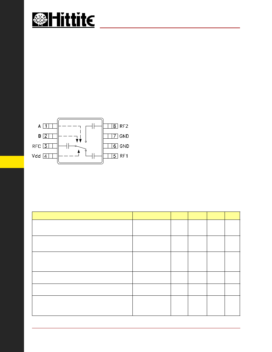
Functional Diagram
Low Cost 5-6 GHz Switch
Ultra Small Package: MSOP8
High Input P1dB: +33 dBm
Single Positive Supply: +3 to +8V
Electrical Specifi cations,
T
A
= +25° C, Vdd = +5 Vdc, 50 Ohm System
Typical Applications
The HMC224MS8 is ideal for:
· UNII & HiperLAN
· PCMCIA WirelessLAN
The HMC224MS8 is a low-cost SPDT switch in
an 8-lead MSOP package for use in transmit-
receive applications. The device can control sig-
nals from 5.0 to 6.0 GHz and is especially suited
for 5.2 GHz UNII and 5.8 GHz ISM applications
with only 1.2 dB loss. The design provides excep-
tional power handling performance; input P1dB =
+33 dBm at 5 Volt bias. RF1 and RF2 are refl ec-
tive shorts when "Off". On-chip circuitry allows
single positive supply operation at very low DC
current with control inputs compatible with CMOS
and most TTL logic families. No DC blocking
capacitors are required on RF I/O ports.
Parameter
Frequency
Min.
Typ.
Max.
Units
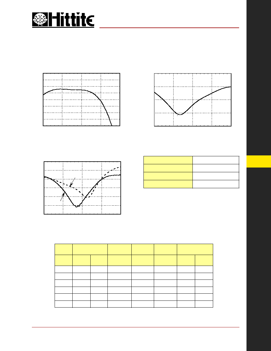
Insertion Loss
5.0 - 6.0 GHz
5.1 - 5.4 GHz
5.4 - 5.9 GHz
1.3
1.2
1.3
1.6
1.5
1.6
dB
dB
dB
Isolation
5.0 - 6.0 GHz
5.1 - 5.4 GHz
5.4 - 5.9 GHz
20
26
22
24
31
27
dB
dB
dB
Return Loss
RF Common
RF1 & RF2
5.0 - 6.0 GHz
5.1 - 5.9 GHz
5.0 - 6.0 GHz
5.1 - 5.9 GHz
11
12
11
11
15
16
14
15
dB
dB
dB
dB
Input Power for 1 dB Compression
0/3V Control
0/5V Control
5.0 - 6.0 GHz
5.0 - 6.0 GHz
27
29
31
33
dBm
dBm
Input Third Order Intercept
0/3V Control
0/5V Control
5.0 - 6.0 GHz
5.0 - 6.0 GHz
31
33
35
37
dBm
dBm
Switching Characteristics
5.0 - 6.0 GHz
tRISE, tFALL (10/90% RF)
tON, tOFF (50% CTL to 10/90% RF)
10
25
ns
ns
MICROWAVE CORPORATION
14 - 73
For price, delivery, and to place orders, please contact Hittite Microwave Corporation:
12 Elizabeth Drive, Chelmsford, MA 01824 Phone: 978-250-3343 Fax: 978-250-3373
Order Online at www.hittite.com
14
SWITCHES - SMT
HMC224MS8
-4
-3.5
-3
-2.5
-2
-1.5
-1
-0.5
0
4
5
6
7
8
INSERTION LOSS (dB)
FREQUENCY (GHz)
-40
-30
-20
-10
0
4
5
6
7
8
ISOLATION (dB)
FREQUENCY (GHz)
-30
-25
-20
-15
-10
-5
0
4
5
6
7
8
RETURN LOSS (dB)
FREQUENCY (GHz)
S11 RFC
S22
Return Loss
Insertion Loss
Isolation
v01.0300
GaAs MMIC T/R SWITCH
5.0 - 6.0 GHz
Truth Table
*Control Input Voltage Tolerances are ± 0.2 Vdc.
Caution: Do not operate in 1dB compression at power levels above +33 dBm and do not "hot switch"
power levels greater than +23 dBm (Vdd = +5Vdc).
DC blocks are not required at ports RFC, RF1 and RF2.
Bias
Control
Input*
Bias Current
Control
Current
Control
Current
Signal
Path State
Vdd
(Vdc)
A
(Vdc)
B
(Vdc)
Idd
(uA)
Ia
(uA)
Ib
(uA)
RF to
RF1
RF to
RF2
3
0
0
10
-5
-5
OFF
OFF
3
0
Vdd
10
-10
0
ON
OFF
3
Vdd
0
10
0
-10
OFF
ON
5
0
0
45
-22
-23
OFF
OFF
5
0
Vdd
45
-5
-40
ON
OFF
5
Vdd
0
115
-40
-5
OFF
ON
Absolute Maximum Ratings
Bias Voltage Range (Vdd)
-0.2 to +12 Vdc
Control Voltage Range (A & B)
-0.2 to Vdd Vdc
Storage Temperature
-65 to +150 °C
Operating Temperature
-40 to +85 °C
MICROWAVE CORPORATION
14 - 74
For price, delivery, and to place orders, please contact Hittite Microwave Corporation:
12 Elizabeth Drive, Chelmsford, MA 01824 Phone: 978-250-3343 Fax: 978-250-3373
Order Online at www.hittite.com
SWITCHES - SMT
14
HMC224MS8
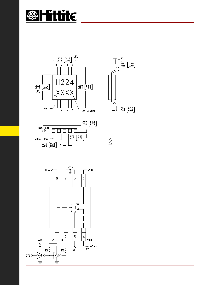
Outline Drawing
v01.0300
GaAs MMIC T/R SWITCH
5.0 - 6.0 GHz
Typical Application Circuit
Notes:
1. Control Inputs A and B can be driven directly with CMOS logic
(HC) with V of 3 to 8 Volts applied to the CMOS logic gates
and to pin 4 of the RF switch.
2. Set V to 5 Volts and use HCT series logic to provide a TTL
driver
interface.
3. Highest RF signal power capability is achieved with V set to
+10V. However, the switch will operate properly (but at
lower RF power capability) at bias voltages down to +3V.
4. RF ByPass: Do not use RF bypass capacitors on Vdd, A or B
ports. Resistors R1, R2, R3 = 100 Ohms should be placed
close to the Vdd, A and B ports. Use resistor size 0402 to
minimize parasitic inductances and capacitances.
5. DC Blocking capacitors are not required for each RF port.
6. Evaluation PCB available.
NOTES:
1. PACKAGE BODY MATERIAL: LOW STRESS INJECTION MOLDED
PLASTIC SILICA AND SILICON IMPREGNATED.
2. LEADFRAME MATERIAL: COPPER ALLOY
3. LEADFRAME PLATING: Sn/Pb SOLDER
4. DIMENSIONS ARE IN INCHES [MILLIMETERS].
5. DIMENSION DOES NOT INCLUDE MOLDFLASH OF 0.15mm PER SIDE.
6. DIMENSION DOES NOT INCLUDE MOLDFLASH OF 0.25mm PER SIDE.
7. ALL GROUND LEADS MUST BE SOLDERED TO PCB RF GROUND.
MICROWAVE CORPORATION
14 - 75
For price, delivery, and to place orders, please contact Hittite Microwave Corporation:
12 Elizabeth Drive, Chelmsford, MA 01824 Phone: 978-250-3343 Fax: 978-250-3373
Order Online at www.hittite.com
14
SWITCHES - SMT
HMC224MS8
v01.0300
GaAs MMIC T/R SWITCH
5.0 - 6.0 GHz
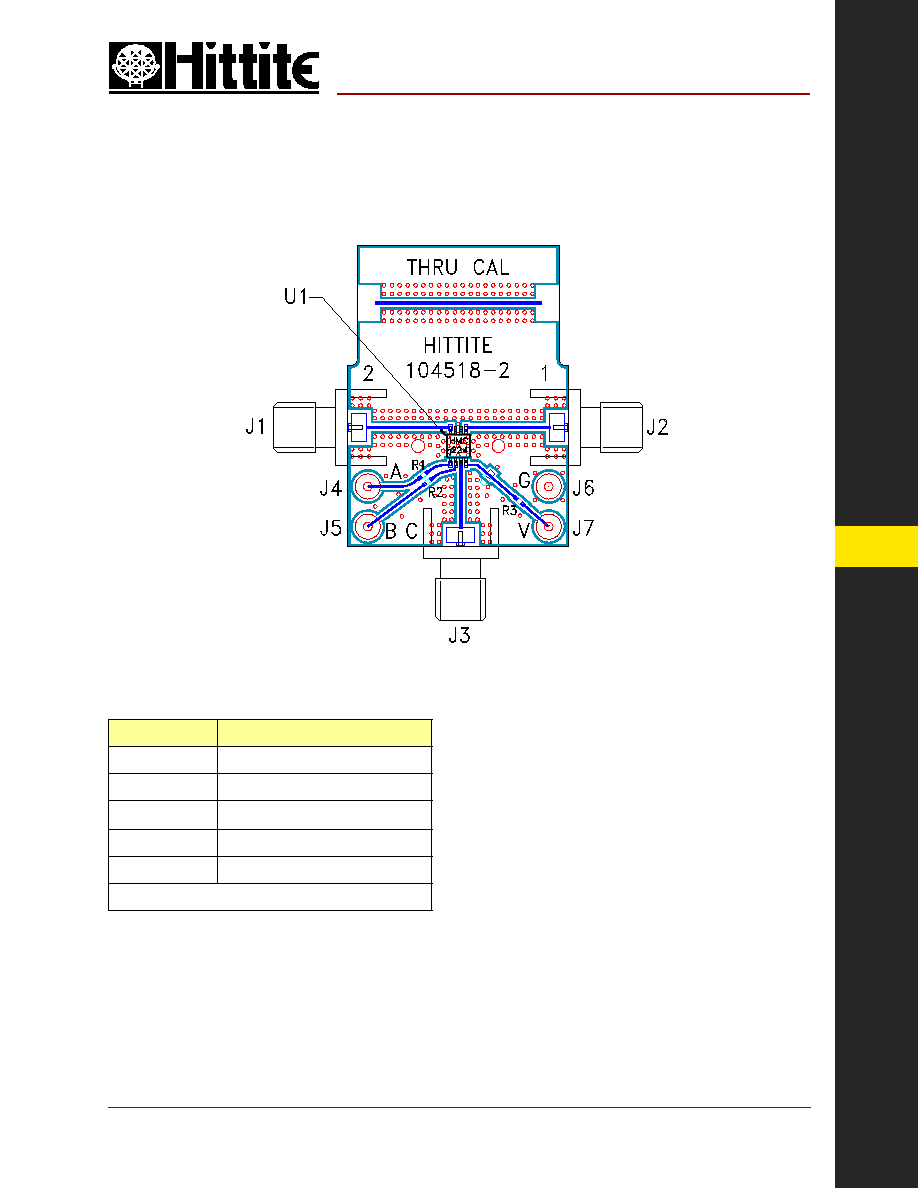
Evaluation PCB
The circuit board used in the fi
nal application
should be generated with proper RF circuit design
techniques. Signal lines at the RF port should
have 50 ohm impedance and the package ground
leads should be connected directly to the ground
plane similar to that shown above. The evalua-
tion circuit board shown above is available from
Hittite Microwave Corporation upon request.
List of Material
Item
Description
J1 - J3
PC Mount SMA RF Connector
J4 - J7
DC Pin
R1, R3
100
resistor, 0402 Pkg.
U1
HMC224MS8 T/R Switch
PCB*
104518 Evaluation PCB
* Circuit Board Material: Rogers 4350