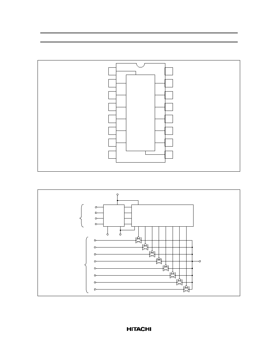
HD74HC4051
8-Channel Analog Multiplexer Demultiplexer
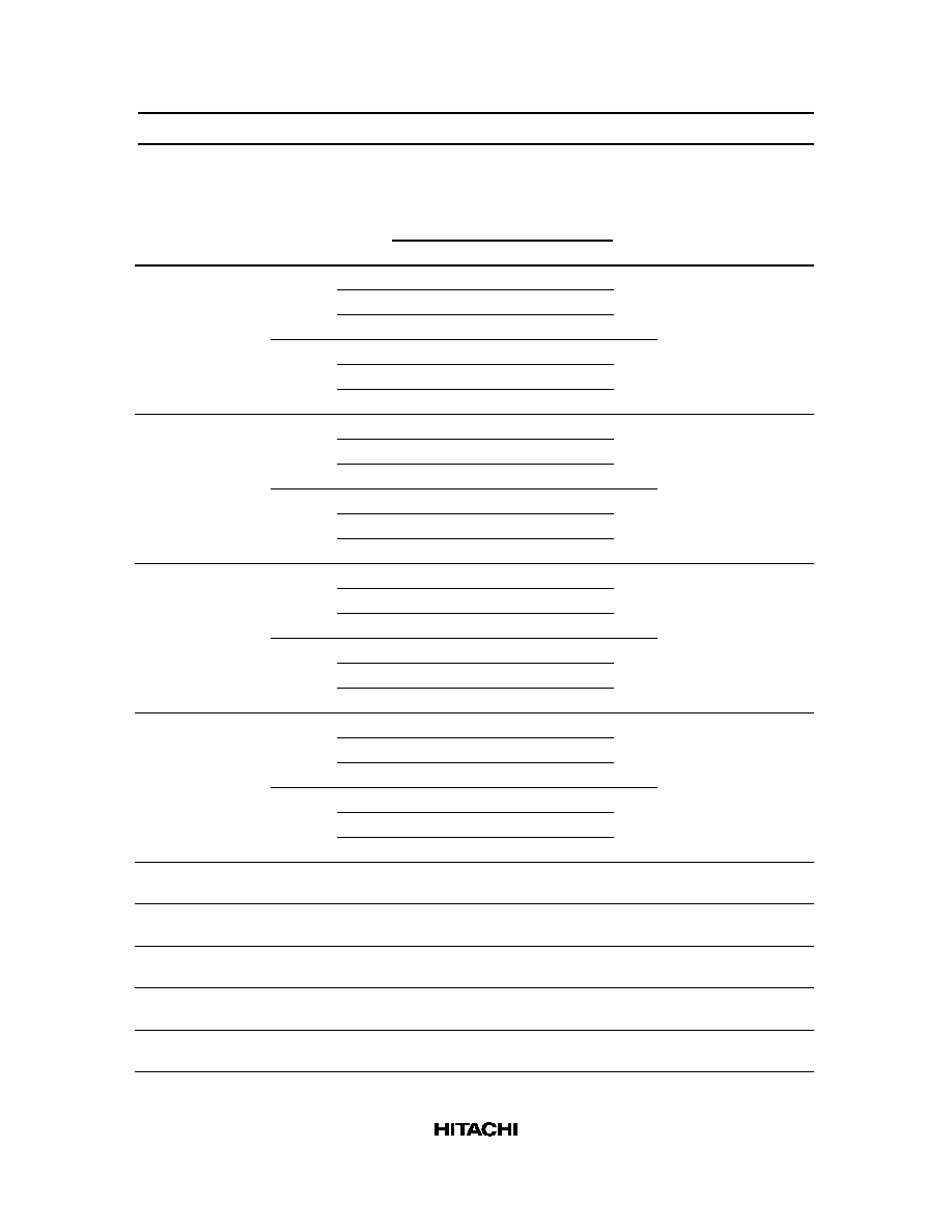
Description
This device connects together the outputs of 8 switches, thus achieving an 8 Channel Multiplexer. The
binary code placed on the A, B, and C select lines determine which one of the eight switches in "on", and
connects one of the eight inputs to the common output.
Features
·
High Speed Operation
·
Wide Operating Voltage
·
Low Quiescent Supply Current
Function Table
Control Inputs
Inhibit
C
B
A
ON Switch
L
L
L
L
X
0
L
L
L
H
X
1
L
L
H
L
X
2
L
L
H
H
X
3
L
H
L
L
X
4
L
H
L
H
X
5
L
H
H
L
X
6
L
H
H
H
X
7
H
X
X
X
--
X :
Don't Care
HD74HC4051
3
Absolute Maximum Ratings
Item
Symbol
Rating
Unit
Supply voltage
V
CC
0.5 to +7.0
V
V
CC
V
EE
0.5 to +7.0
V
Control input voltage
V
IN
GND 0.5 to V
CC
+ 0.5
V
Switch I/O voltage
V
I/O
V
EE
0.5 to V
CC
+ 0.5
V
Supply current
(V
CC
)
I
CC
+50
mA
(GND)
I
GND
50
mA
Switch I/O current (per pin)
I
I/O
±
25
mA
Control input diode current
I
IK
±
20
mA
Switch I/O diode current
I
IOK
±
20
mA
Power dissipation
P
T
500
mW
Storage temperature range
Tstg
65 to +150
°
C
Recommended Operating Range
Item
Symbol
Min
Typ
Max
Unit
Supply voltage
V
CC
V
EE
2
--
6
V
V
GND
V
EE
4
--
0
V
Control input voltage
V
IN
0
--
V
CC
V
Switch I/O voltage
V
I/O
V
EE
--
V
CC
V
Operating temperature
Topr
40
--
+85
°
C
Input rise/fall time
V
CC
= 2.0 V
t
r
, t
f
0
--
1000
ns
V
CC
= 4.5 V
0
--
500
ns
V
CC
= 6.0 V
0
--
400
ns
HD74HC4051
4
DC Characteristics (V
SS
= V
EE
= GND)
Ta = 25
°
C
Ta = 40 to
+85
°
C
Item
Symbol
V
CC
(V) Min
Typ
Max
Min
Max
Unit
Test Conditions
Control input voltage V
IH
2.0
1.5
--
--
1.5
--
V
4.5
3.15
--
--
3.15
--
6.0
4.2
--
--
4.2
--
V
IL
2.0
--
--
0.5
--
0.5
V
4.5
--
--
1.35
--
1.35
6.0
--
--
1.8
--
1.8
ON resistance
R
ON
2.0
--
2000
5000 --
6250
V
INH
= V
IL
4.5
--
120
180
--
225
V
I/O
= V
CC
to V
EE
6.0
--
100
170
--
210
I
I/O
2 mA
2.0
--
200
800
--
1000
V
INH
= V
IL
4.5
--
80
150
--
190
V
I/O
= V
CC
to V
EE
6.0
--
70
140
--
175
V
I/O
2 mA
ON resistance
R
ON
2.0
--
50
--
--
--
V
INH
= V
IL
between any two
4.5
--
13
40
--
50
V
I/O
= V
CC
to V
EE
channels
6.0
--
10
20
--
25
I
I/O
2 mA
OFF channel
leakage current
(switch off)
I
S (OFF)
6.0
--
--
±
0.1
--
±
1.0
µ
A
V
INH
= V
IL
OFF channel
leakage current
(switch on)
I
S (ON)
6.0
--
--
±
0.1
--
±
1.0
µ
A
V
INH
= V
IL
Control input current Iin
6.0
--
--
±
0.1
--
±
1.0
µ
A
Vin = V
CC
or V
SS
Quiescent supply
current
I
CC
6.0
--
--
4.0
--
40
µ
A
Vin = V
CC
or V
SS