
HD404054 Series/HD404094 Series
Rev. 6.0
Sept. 1998
Description
The HD404054 Series and HD404094 Series are HMCS400-series microcomputers designed to increase
program productivity with large-capacity memory. Each microcomputer has three timers, one serial
interface, comparator, input capture circuit.
The HD404054 Series includes three chips: the HD404052 with 2-kword ROM; the HD404054 with 4-
kword ROM; and the HD4074054 with 4-kword PROM (ZTAT
TM
version). Also, the HD404094 Series
includes three chips: the HD404092 with 2-kword ROM; the HD404094 with 4-kword ROM; and the
HD4074094 with 4-kword PROM (ZTAT
TM
version).
The HD4074054 and HD4074094 are PROM version (ZTAT
TM
microcomputers). Program can be written
to the PROM by a PROM writer, which can dramatically shorten system development periods and smooth
the process from debugging to mass production. (The ZTAT
TM
version is 27256-compatible.)
Features
�
The differences between HD404054 Series and HD404094 Series
HD404054 Series
HD404094 Series
I/O pins
10 large-current output pins: Six 15-mA sinks
and four 10-mA sources
�
6 largecurrent output pins: Two 15-mA
sinks and four 10-mA sources
�
4 intermediate voltage output pins
�
27 I/O pins and 8 dedicated input pins
�
Three timer/counters
�
Eight-bit input capture circuit
�
Two timer outputs (including two PWM outputs)
�
One event counter inputs (including one double-edge function)
�
One clock-synchronous 8-bit serial interface
�
Comparator (2 channels)
�
Built-in oscillators
Main clock: Ceramic or crystal oscillator (an external clock is also possible)

HD404054 Series/HD404094 Series
2
�
Six interrupt sources
Two by external sources
Four by internal sources
�
Subroutine stack up to 16 levels, including interrupts
�
Two low-power dissipation modes
Standby mode
Stop mode
�
One external input for transition from stop mode to active mode
�
Instruction cycle time: 1
�
s (f
OSC
= 4 MHz at 1/4 division ratio)
1/4, or 1/32 division ratio can be selected by hardware
�
Two operating modes
MCU mode
MCU/PROM mode (HD4074054, HD4074094)
Ordering Information
Product Name
Type
HD404054 Series
HD404094 Series
ROM (words)
RAM (digit)
Package
Mask ROM
HD404052H
HD404092H
2,048
512
FP-44A
HD404052S
HD404092S
DP-42S
HD40A4052H
FP-44A
HD40A4052S
DP-42S
HD404054H
HD404094H
4,096
FP-44A
HD404054S
HD404094S
DP-42S
HD40A4054H
FP-44A
HD40A4054S
DP-42S
ZTAT
TM
HD4074054H
HD4074094H
4,096
FP-44A
HD4074054S
HD4074094S
DP-42S
ZTAT
TM
: Zero Turn Around Time ZTAT is a trademark of Hitachi, Ltd.

HD404054 Series/HD404094 Series
3
Pin Arrangement
RD /COMP
RD /COMP
RD
RD
RC
RE /VC
ref
TEST
OSC
OSC
RESET
GND
D
D
D
D
D
D
D
D
D
D
0 0
1 1
2
3
0
0
1
2
0
1
2
3
4
5
6
7
8
9
1
2
3
4
5
6
7
8
9
10
11
12
13
14
15
16
17
18
19
20
21
42
41
40
39
38
37
36
35
34
33
32
31
30
29
28
27
26
25
24
23
22
DP-42S
CC
3 1
2 1
1 1
0
3
2
1
0
3
2
1
0
3
2
1
0
0 1
13 0
12
1
2
3
4
5
6
7
8
9
10
11
33
32
31
30
29
28
27
26
25
24
23
44
43
42
41
40
39
38
37
36
35
34
12
13
14
15
16
17
18
19
20
21
22
FP-44A
RE
0
/VC
ref
TEST
OSC
1
OSC
2
RESET
GND
D
D
D
D
D
R4 /EVND
R3
R3 /TOD
R3 /TOC
R3
R2
R2
R2
R2
R1
R1
0
3
2
1
0
3
2
1
0
3
2
5
6
7
8
9
12
13 0
0
1
NC
RC
0
3
2
1 1
0 0
CC
Top view
3 1
2 1
1 1
1
0
0
1
2
3
4
V
SEL
R4 /SO
R4 /SI
R4 /
SCK
R4 /EVND
R3
R3 /TOD
R3 /TOC
R3
R2
R2
R2
R2
R1
R1
R1
R1
R0 /
INT
D /
INT
D /
STOPC
RD
RD
RD /COMP
RD /COMP
V
SEL
R4 /SO
R4 /SI
R4 /
SCK
D
D
D
D
D
D /
STOPC
D /
INT
R0 /
INT
R1
R1
NC

HD404054 Series/HD404094 Series
4
Pin Description
Pin Number
Item
Symbol
DP-42S
FP-44A
I/O
Function
Power supply V
CC
42
38
Applies power voltage
GND
11
6
Connected to ground
Test
TEST
7
2
I
Used for factory testing only: Connect this pin to V
CC
Reset
RESET
10
5
I
Resets the MCU
Oscillator
OSC
1
8
3
I
OSC
2
9
4
O
Port
D
0
�D
9
12�21
7�16
I/O
*
Input/output pins addressed by individual bits; pins
D
0
�D
3
are high-current source pins that can each
supply up to 10 mA.
The HD404054 Series: pins D
4
�D
9
are high-current
sink pins that can each supply up to 15mA.
The HD404094 Series: D
4
�D
7
are intermediate
voltage (12 V) NMOS open-drain pins, and D
8
, D
9
are
high-current sink pins that can each supply up to 15
mA.
D
12
,D
13
22, 23
17, 18
I
Input pins addressable by individual bits
R0
0
�R4
3
24�40
19�36
I/O
Input/output pins addressable in 4-bit units
RD
0
�RD
3
,
RC
0
, RE
0
1�6
39�43,1
I
Input pins addressable in 4-bit units
Interrupt
INT
0
,
INT
1
23, 24
18, 19
I
Input pins for external interrupts
Stop clear
STOPC
22
17
I
Input pin for transition from stop mode to active mode
Serial
SCK
1
38
34
I/O
Serial clock input/output pin
SI
1
39
35
I
Serial receive data input pin
SO
1
40
36
O
Serial transmit data output pin
Timer
TOC, TOD 34, 35
30, 31
O
Timer output pins
EVND
37
33
I
Event count input pins
Comparator
COMP
0
,
COMP
1
1, 2
39, 40
I
Analog input pins for voltage comparator
VC
ref
6
1
Reference voltage pin for inputting the threshold
voltage of the analog input pin.
Division rate
SEL
41
37
I
Input pin for selecting system clock division rate after
RESET
input or after stop mode cancellation.
1/4 division rate: Connect it to V
CC
1/32 division rate: Connect it to GND
Note:
*
D
4
�D
7
of the HD404094 Series are output pins.
HD404054 Series/HD404094 Series
5
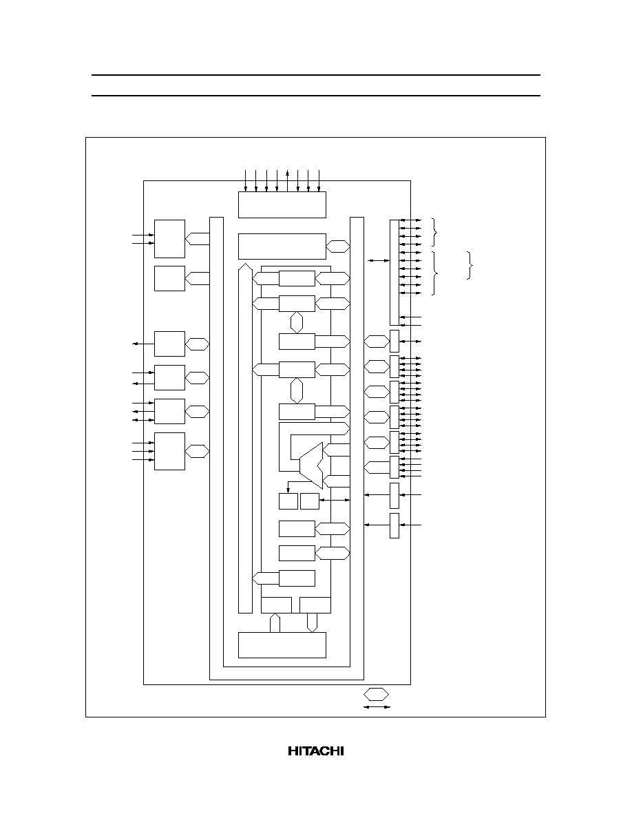
Block Diagram
RESET
TEST
STOPC
OSC
OSC
SEL
V
GND
System control
RAM
(512 4bit)
�
W (2bit)
X (4bit)
SPX (4bit)
Y (4bit)
SPY (4bit)
ST
(1bit)
CA
(1bit)
A (4bit)
B (4bit)
SP (10bit)
Instruction
decoder
PC (14bit)
ROM
(4,096 10bit)
(2,048 10bit)
�
�
Internal address bus
Internal data bus
External
interrupt
Timer
A
Timer
C
Timer
D
Serial
1
Compa-
rator
D port
R0 port
R1 port
R2 port
R3 port
R4 port
RD port
RC port
: Data bus
: Signal line
ALU
High
current
source
pins
High
current
sink pins
Intermediate
voltage NMOS
open-drain
output pins
*
CPU
D
D
D
D
D
D
D
D
D
D
D
D
0
1
2
3
4
5
6
7
8
9
12
13
R0
0
R1
R1
R1
R1
0
1
2
3
R2
R2
R2
R2
0
1
2
3
R3
R3
R3
R3
0
1
2
3
R4
R4
R4
R4
0
1
2
3
RD
RD
RD
RD
0
1
2
3
RC
0
0
1
TOC
EVND
TOD
INT
INT
1
1
1
SI
SO
SCK
0
1
VC
ref
COMP
COMP
1
2
CC
Internal data bus
RE port
RE
0
Note: Only HD404094 Series
*