
DS07-16202-2E
FUJITSU SEMICONDUCTOR
DATA SHEET
32-bit Proprietary Microcontroller
CMOS
FR Family MB91191/192 Series
MB91191R/MB91192/MB91F191A/MB91F192
s
s
s
s
DESCRIPTION
The MB91191/192 series is a single-chip microcontroller using a 32-bit RISC-CPU (FR series) as its core. It
contains peripheral I/O resources suitable for software servo control in applications such as VTRs that require
high-speed CPU processing.
s
s
s
s
FEATURES
CPU
· 32-bit RISC (FR series) , load/store architecture, 5-stage pipeline
· General-purpose registers : 16
×
32-bit
· 16-bit fixed-length instructions (basic instructions) , 1 instruction per cycle
· Includes memory-to-memory transfer, bit manipulation, and barrel shift instructions :
Optimized for embedded applications
· Includes function entry/exit instructions and multiple-register load/store instructions :
Instruction set supports high level languages
· Register interlock function : For efficient assembly language coding
· Branch instructions with delay slots : Reduced overhead for branch operations
· Internal multiplier unit is supported at instruction level
Signed 32-bit multiplication : 5 cycles
Signed 16-bit multiplication : 3 cycles
· Interrupts (PC and PS saving) : 6 cycles, 16 priority levels
(Continued)
s
s
s
s
PACKAGE
Plastic, LQFP, 120-pin
(FPT-120P-M05)
Plastic, FLGA, 144-pin
(LGA-144P-M02)

MB
91191/192 Series
2
Bus Interface
· 16-bit address output, 8/16-bit data input and output
· Basic bus cycle : 2 clock cycles
· Supports interfaces for various types of memory
· Multiplexed data/address input/output
· Automatic wait cycles : Between 0 and 7 wait cycles can be specified independently for each memory area
· Unused data/address pins can be configured as input/output ports
· Supports little endian mode
Bit Search Module
· Searches, starting from the MSB, for the position of the first 1/0 bit transition in a word. The operation is
performed in one cycle.
Serial I/O
· 3 channels with internal buffer RAM (automatic transfer of up to 128 bytes)
· Independent send and receive buffer mode (automatic transfer of up to 64 bytes)
A/D Converter (Successive Approximation Type)
· 10-bit
×
16 channels
· Uses successive approximation conversion method (conversion time : 8.4
µ
s @ 20 MHz)
· Channel scan function
· Hardware and software conversion start functions
· Internal FIFO (Software conversion : 6 stages, Hardware conversion : 6 stages)
Timers
· 16-bit
×
4 channels
· 16-bit timer/counter
×
1 channel (with square wave output)
· 8/16-bit timer/counter
×
1 channel (with square wave output)
FG input unit
· Incorporates capstan, drum, and reel input circuits
Capture unit
· Internal 24-bit free-run counter (Minimum resolution
=
50 ns @ 20 MHz)
· Internal FIFO (Data : 21-bit
×
8, Detection : 8-bit
×
8)
Programmable pattern generator
· Internal RAM buffer (PPG0 : 256 bytes, PPG1 : 64 bytes)
· Output timing resolution : 800 ns @ 20 MHz
· Includes an A/D converter hardware start function
Realtime timing generator
· RTG : 3 circuits
· Output timing resolution : 400 ns or 800 ns selectable
· Timing output ports : 5 ports
PWM
· 12-bit PWM
×
6 channels (rate, multi-type)
· Base frequency
=
78.1 kHz or 39.0 kHz (@ 20 MHz) selectable
(Continued)

MB
91191/192 Series
3
(Continued)
PWC
· 8-bit PWC
×
1 channel (with mask input)
· Measurement resolution : 400 ns @ 20 MHz
General-purpose prescaler
· 10-bit prescaler
×
1 channel (with square wave and pulse outputs)
· Dedicated internal oscillator circuit
· Includes load function driven by PPG output
Interrupt control
· External interrupts : 3 inputs
· Key input interrupt : 8 inputs
MB
91191/192 Series
4
s
s
s
s
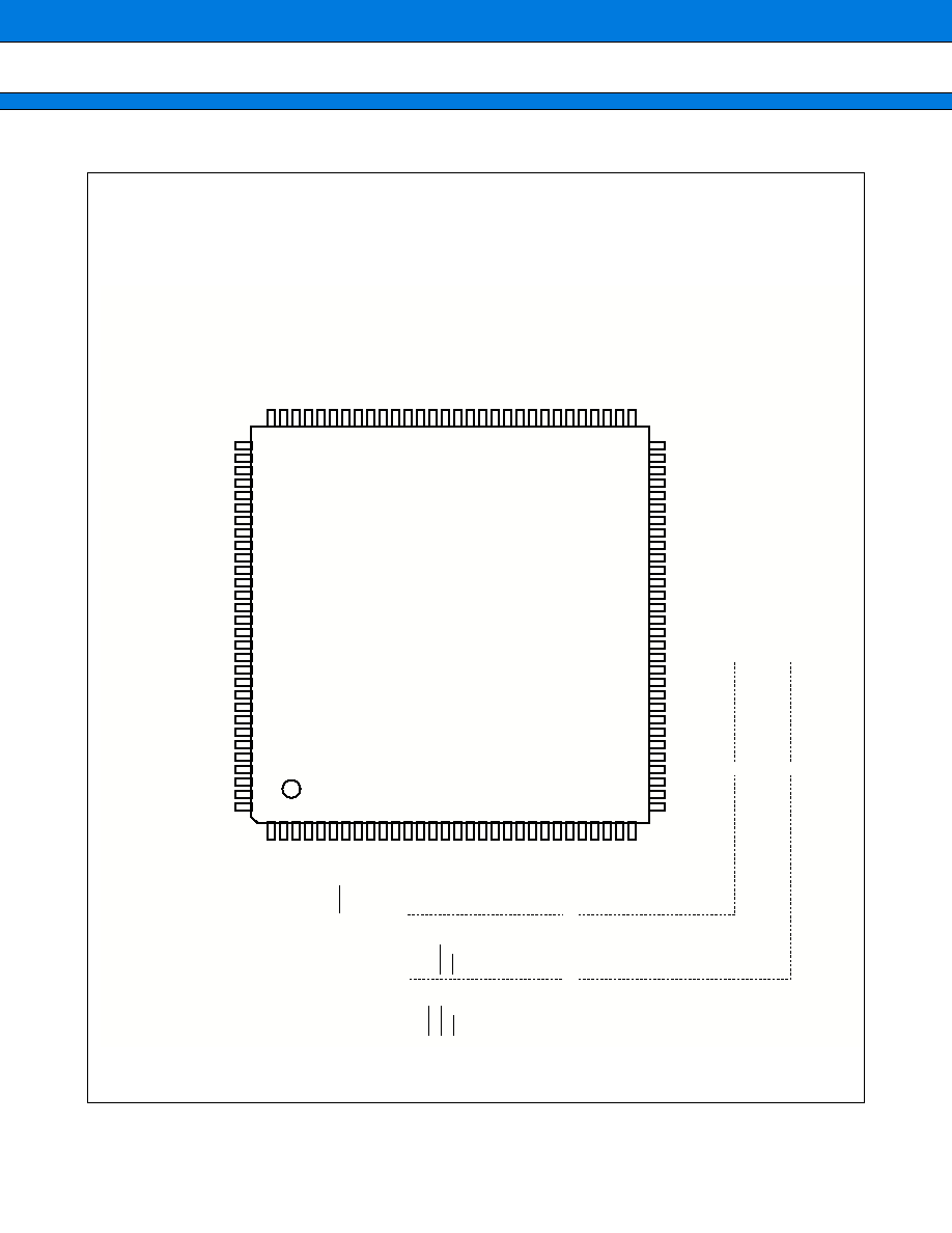
PIN ASSIGNMENT
(Continued)
PA0/AN-8/KEY0
PB7/AN-7
PB6/AN-6
PB5/AN-5
PB4/AN-4
PB3/AN-3
PB2/AN-2
PB1/AN-1
PB0/AN-0
AV
DD
AV
RH
AV
SS
V
SS
P17/RTG4
P16/RTG3
P15/RTG2
P14/RTG1
P13/RTG0
P12/EC5/INT1
P11/EC4/INT0
P10/PMSK
P07/EXI2/PMI
P06/EXI1
P05/EXI0
P04/CFG
P03/DFG
P02/DPG
P01/RFG0
P00/RFG1
V
DD
P93/PPG02
P94/PPG03
P80/PPG04
P81/PPG05
P82/PPG06
P83/PPG07
P84/PPG08
P85/PPG09
P86/PPG10
P87/PPG11
P40/PPG12
P41/PPG13
P42/PPG14
P43/PPG15
P44/PPG16
P45/PPG17
P46/PPG18
P47
P57
P56
P55
P54
P53
P52
P51
P50
V
SS
P37
P36
P35
A15
A14
A13
A12
A11
A10
A09
A08
D31/A07
D30/A06
D29/A05
P57
P56
P55
P54
P53
P52
P51
P50
D31/A15
D30/A14
D29/A13
PA1/AN-9/KEY1
PA2/AN-A/KEY2
PA3/AN-B/KEY3
PA4/AN-C/KEY4
PA5/AN-D/KEY5
PA6/AN-E/KEY6
PA7/AN-F/KEY7
PD0/SI2
PD1/SO2
PD2/SCK2
PD3/SI1/INT2
PD4/SO1
PD5/SCK1
PD6/SCS0
PD7/SI0
PC0/SO0
PC1/SCK0
PC2/PWM5/SCS1
PC3/PWM4/SCS2
PC4/PWM3
PC5/PWM2
PC6/PWM1
PC7/PWM0
V
SS
OSCI/PCK
OSCO
V
DD
P90/P0
P91/PPG00
P92/PPG01
ALE
WR1
WR0
RD
A00/D16
A01/D17
A02/D18
A03/D19
A04/D20
A05/D21
A06/D22
A07/D23
A08/D24
A09/D25
A10/D26
A11/D27
A12/D28
ALE
P62
WR0
RD
P20
P21
P22
P23
P24
P25
P26
P27
A00/D24
A01/D25
A02/D26
A03/D27
A04/D28
X0
X1
V
SS
MD2
MD1
MD0
RST
P70/XOUT
P67/T40
P66/T501
P65
P64
P63
P62
P61
P60
P20
P21
P22
P23
P24
P25
P26
P27
V
DD
P30
P31
P32
P33
P34
16-bit MPX mode
8-bit MPX mode
95
100
105
110
115
120
90
85
80
75
70
65
5
10
15
20
25
30
60
55
50
45
40
35
(TOP VIEW)
(FPT-120P-M05)

MB
91191/192 Series
5
(Continued)
Top View
65
OSCO
66
OSCI
30
P34
28
P32
29
P33
64
V
DD
68
PC7
69
PC6
27
P31
25
V
DD
26
P30
67
V
SS
71
PC4
72
PC3
24
P27
22
P25
23
P26
70
PC5
74
PC1
75
PC0
21
P24
19
P22
20
P23
73
PC2
77
PD6
76
PD7
18
P21
16
P60
17
P20
78
PD5
80
PD3
79
PD4
13
P63
15
P61
14
P62
81
PD2
83
PD0
82
PD1
10
P66
12
P64
11
P65
84
PA7
86
PA5
85
PA6
7
RST
9
P67
8
P70
87
PA4
89
PA2
88
PA3
4
MD2
6
MD0
5
MD1
90
PA1
32
P36
59
P94
56
P82
53
P85
50
P40
47
P43
44
P46
41
P56
38
P53
35
P50
33
P37
58
P80
55
P83
52
P86
49
P41
46
P44
45
P45
42
P57
39
P54
36
P51
62
P91
63
P90
31
P35
61
P92
60
P93
57
P81
54
P84
51
P87
48
P42
43
P47
40
P55
37
P52
34
V
SS
1
X0
3
V
SS
2
X1
91
PA0
94
PB5
97
PB2
100
AV
DD
103
V
SS
108
P13
111
P10
114
P05
117
P02
120
V
DD
93
PB6
96
PB3
99
PB0
102
AV
SS
105
P16
106
P15
109
P12
112
P07
115
P04
118
P01
92
PB7
95
PB4
98
PB1
101
AV
RH
104
P17
107
P14
110
P11
113
P06
116
P03
119
P00
(LGA-144P-M02)
Note : The FLGA-144 package is not supplied for the MB91191 series.
It is supplied only for the MB91192 series.

MB
91191/192 Series
6
s
s
s
s
PIN DESCRIPTIONS
(Continued)
Pin No.
Pin Name
Circuit
Type
Function
1
X0
(I)
A
Crystal oscillator pins
2
X1
(O)
3
V
SS
V
SS
pin
4
MD2
B
Operation mode setting pins
CMOS Schmitt inputs
5
MD1
6
MD0
7
RST
B
Reset input pin. CMOS Schmitt input.
8
P70/XOUT
C
Shared pin with clock output (X0/2, PCK/2) . CMOS input.
9
P67/T40
C
Shared pin with timer 4 square wave output. CMOS input.
10
P66/T501
Shared pin with timer 5 square wave output. CMOS input.
11
P65
General-purpose I/O port. CMOS input.
12
P64
General-purpose I/O port. CMOS input.
13
P63/ALE/ALE
Shared pin with address strobe output. CMOS input.
14
P62/P62/WR1
Shared pin with write strobe output 1. CMOS input.
15
P61/WR0/WR0
Shared pin with write strobe output 0. CMOS input.
16
P60/RD/RD
Shared pin with read strobe output. CMOS input.
17
P20/P20/D16 : A00
C
General-purpose I/O ports.
CMOS inputs.
18
P21/P21/D17 : A01
19
P22/P22/D18 : A02
20
P23/P23/D19 : A03
21
P24/P24/D20 : A04
22
P25/P25/D21 : A05
23
P26/P26/D22 : A06
24
P27/P27/D23 : A07
25
V
DD
Power supply pin
26
P30/D24 : A00/D24 : A08
C
Shared external bus pins and high-current I/O ports.
CMOS inputs.
27
P31/D25 : A01/D25 : A09
28
P32/D26 : A02/D26 : A10
29
P33/D27 : A03/D27 : A11
30
P34/D28 : A04/D28 : A12
31
P35/D29 : A05/D29 : A13
32
P36/D30 : A06/D30 : A14
33
P37/D31 : A07/D31 : A15
34
V
SS
V
SS
pin

MB
91191/192 Series
7
(Continued)
Pin No.
Pin Name
Circuit
Type
Function
35
P50/A08/P50
C
Shared external bus pins and high-current I/O ports.
CMOS inputs.
36
P51/A09/P51
37
P52/A10/P52
38
P53/A11/P53
39
P54/A12/P54
40
P55/A13/P55
41
P56/A14/P56
42
P57/A15/P57
43
P47
C
General-purpose I/O port. CMOS input.
44
P46/PPG18
Shared pins with PPG outputs.
CMOS inputs.
45
P45/PPG17
46
P44/PPG16
47
P43/PPG15
48
P42/PPG14
49
P41/PPG13
50
P40/PPG12
51
P87/PPG11
C
Shared pins with PPG outputs.
CMOS inputs.
52
P86/PPG10
53
P85/PPG09
54
P84/PPG08
55
P83/PPG07
56
P82/PPG06
57
P81/PPG05
58
P80/PPG04
59
P94/PPG03
C
Shared pins with PPG outputs.
CMOS inputs.
60
P93/PPG02
61
P92/PPG01
C
Shared pins with PPG outputs.
CMOS inputs.
62
P91/PPG00
63
P90/P0
Shared pin with general-purpose prescaler output. CMOS input.
64
V
DD
Power supply pin
65
OSCO
(O)
A
Crystal oscillator pins for dedicated general-purpose prescaler
oscillation.
66
OSCI/PCK
(I)
67
V
SS
V
SS
pin

MB
91191/192 Series
8
(Continued)
Pin No.
Pin Name
Circuit
Type
Function
68
PC7/PWM0
C
Shared pins with PWM outputs.
CMOS inputs.
69
PC6/PWM1
70
PC5/PWM2
71
PC4/PWM3
72
PC3/PWM4/SCS2
F
Shared pin with PWM output and serial 2 chip select.
CMOS Schmitt input.
73
PC2/PWM5/SCS1
Shared pin with PWM output and serial 1 chip select.
CMOS Schmitt input.
74
PC1/SCK0
Shared pin with serial 0 shift clock.
CMOS Schmitt input.
75
PC0/SO0
C
Shared pin with serial 0 serial output. CMOS input.
76
PD7/SI0
F
Shared pin with serial 0 serial input.
CMOS Schmitt input.
77
PD6/SCS0
Shared pin with serial 0 chip select input.
CMOS Schmitt input.
78
PD5/SCK1
Shared pin with serial 1 shift clock.
CMOS Schmitt input.
79
PD4/SO1
C
Shared pin with serial 1 serial output. CMOS input.
80
PD3/SI1/INT2
F
Shared pin with serial 1 serial input and external interrupt 2.
CMOS Schmitt input.
81
PD2/SCK2
Shared pin with serial 2 shift clock.
CMOS Schmitt input.
82
PD1/SO2
C
Shared pin with serial 2 serial output. CMOS input.
83
PD0/SI2
F
Shared pin with serial 2 serial input.
CMOS Schmitt input.
84
PA7/AN-F/KEY7
E
Shared pins with analog inputs and key inputs.
CMOS Schmitt inputs
85
PA6/AN-E/KEY6
86
PA5/AN-D/KEY5
87
PA4/AN-C/KEY4
88
PA3/AN-B/KEY3
89
PA2/AN-A/KEY2
90
PA1/AN-9/KEY1
91
PA0/AN-8/KEY0

MB
91191/192 Series
9
(Continued)
Pin No.
Pin Name
Circuit
Type
Function
92
PB7/AN-7
D
Shared pins with analog inputs.
CMOS Schmitt inputs.
93
PB6/AN-6
94
PB5/AN-5
95
PB4/AN-4
96
PB3/AN-3
97
PB2/AN-2
98
PB1/AN-1
99
PB0/AN-0
100
AV
DD
A/D converter power supply pin
101
AV
RH
A/D converter reference power supply pin
102
AV
SS
A/D converter V
SS
pin
103
V
SS
V
SS
pin
104
P17/RTG4
C
Shared pins with RTG outputs.
CMOS inputs.
105
P16/RTG3
106
P15/RTG2
107
P14/RTG1
108
P13/RTG0
109
P12/EC5/INT1
F
Shared pin with timer 5 clock input and external interrupt input.
CMOS Schmitt input.
110
P11/EC4/INT0
Shared pin with timer 4 clock input and external interrupt input.
CMOS Schmitt input.
111
P10/PMSK
Shared pin with PWC mask input. CMOS Schmitt input.
112
P07/EXI2/PMI
F
Shared pin with external capture input and PWC input.
CMOS Schmitt input.
113
P06/EXI1
Shared pin with external capture input.
CMOS Schmitt input.
114
P05/EXI0
115
P04/CFG
Shared pin with capstan FG input. CMOS Schmitt input.
116
P03/DFG
Shared pin with drum FG input. CMOS Schmitt input.
117
P02/DPG
Shared pin with drum pulse input. CMOS Schmitt input.
118
P01/RFG0
Shared pins with reel FG inputs.
CMOS Schmitt inputs.
119
P00/RFG1
120
V
DD
Power supply pin

MB
91191/192 Series
10
s
s
s
s
I/O CIRCUITS
(Continued)
Type
Circuit
Remarks
A
· Oscillation feedback
resistor : 1 M
approx.
B
· CMOS Schmitt input
C
· CMOS level output
· CMOS input
No standby control
D
· CMOS level output
· CMOS input
with input control
· Analog input
X0,OSCI
X1,OSCO
Clock input
Standby control signal
Input
Standby control signal
=
1 (fixed)
Output data
Input
DC test
DC test
Input control
Output data
DC test
DC test
Analog input
CH selection
Digital input

MB
91191/192 Series
11
(Continued)
Type
Circuit
Remarks
E
· CMOS level output
· CMOS Schmitt input
with input control
· Analog input
F
· CMOS level output
· CMOS Schmitt input
No standby control
H
· CMOS level output
· CMOS Schmitt input
No standby control
Input control
Input data
DC test
DC test
Analog input
CH selection
Digital input
Standby control signal
=
1 (fixed)
Output data
Input
DC test
DC test
Output data
Input
DC test
DC test

MB
91191/192 Series
12
s
s
s
s
BLOCK DIAGRAM
P47
P46/PPG18
P45/PPG17
P44/PPG16
P43/PPG15
P42/PPG14
P41/PPG13
P40/PPG12
P87/PPG11
P86/PPG10
P85/PPG09
P84/PPG08
P83/PPG07
P82/PPG06
P81/PPG05
P80/PPG04
P94/PPG03
P93/PPG02
P92/PPG01
P91/PPG00
P90/P0
PD0/SI2
PD1/SO2
PD2/SCK2
PD3/SI1/INT2
PD4/SO1
PD5/SCK1
PD6/SCS0
PD7/SI0
PC0/S00
PC1/SCK0
PC2/PWM5/SCS1
PC3/PWM4/SCS2
PC4/PWM3
PC5/PWM2
PC6/PWM1
PC7/PWM0
PA7/AN-F/KEY7
PA6/AN-E/KEY6
PA5/AN-D/KEY5
PA4/AN-C/KEY4
PA3/AN-B/KEY3
PA2/AN-A/KEY2
PA1/AN-9/KEY1
PA0/AN-8/KEY0
PB7/AN-7
PB6/AN-6
PB5/AN-5
PB4/AN-4
PB3/AN-3
PB2/AN-2
PB1/AN-1
PB0/AN-0
MD0
MD1
MD2
RST
P37/D31
P30/D24
P27/D23
P20/D16
P57/A15
P50/A08
P60/RD
P61/WR0
P62/WR1
P63/ALE
P64
P65
P66/T501
P67/T40
P17/RTG4
P16/RTG3
P15/RTG2
P14/RTG1
P13/RTG0
P12/EC5/INT1
P11/EC4/INT0
P10/PMSK
P07/EXI2/PMI
P06/EXI1
P05/EXI0
P04/CFG
P03/DFG
P02/DPG
P01/RFG0
P00/RFG1
P70/XOUT
X0
X1
OSCI
OSCO
Mode control
Port 2/3
Port 5
Port 6
Port 7
Port 1
Port 0
OSC
OSC
FR20 CPU core
I-bus
I-bus
D-bus
D-bus
D-bus
C-bus
RAM 2 KB
External bus control
16-bit timers 0 to 3
8/16-bit timer
16-bit timer 4
8-bit PWC
Interrupt
controller
CFG
DFG
RFG0
RFG1
C-unit
10-bit programmable
prescaler
24-bit
FRC
FIFO
29-bit
×
8
RAM 256 byte PPG0
PPG1
RAM 64 byte
Bit search
R-bus
RAM
128 byte
Serial
ch 0
RAM
128 byte
Serial
ch 1
RAM
128 byte
Serial
ch 2
12-bit PWM00-02
12-bit PWM10-12
External interrupts
16-bit RTG0-2
External interrupts
(key inputs)
10-bit A/DC
FIFO
(software)
FIFO
(hardware)
Port 4
Port 8/9
Port C/D
Port A/B
INT2 to INT0 (from port 1, D)
RTG4 to RTG0 (to port 1)
MB91191R
MB91192
MB91F191A
MB91F192
:RAM 6 KB
:RAM 8 KB
:RAM 6 KB
:RAM 8 KB
MB91191R
MB91192
MB91F191A
MB91F192
:ROM 254 KB
:ROM 384 KB
:FLASH 254 KB
:FLASH 384 KB
to
to
to

MB
91191/192 Series
13
(Bus names)
· I bus : 16-bit bus for internal instructions. As the FR family of CPUs use the Harvard architecture, instructions
and data use separate buses. A bus converter is connected to the I bus.
· D bus : Internal 32-bit data bus. The internal peripherals are connected to the D bus.
· C bus : Internal multiplexed bus. Connected to the I and D buses via a switch. An external interface module
is connected to the C bus. Data and instructions are multiplexed on the external data bus.
· R bus : Internal 16-bit data bus. The R bus connects to the D bus via an adapter. The I/O, clock oscillator, and
interrupt controller are connected to the R bus. As the R bus is only 16 bits wide, address and data
are multiplexed on the bus and therefore multiple cycles are required when the CPU accesses these
resources.

MB
91191/192 Series
14
s
s
s
s
MEMORY MAP
I/O area
PPG0 Data RAM area
256 bytes
SIO0 Data RAM area
128 bytes
PPG1 Data RAM area
64 bytes
I/O area
I/O area
Access inhibited
SIO1 Data RAM area
128 bytes
SIO2 Data RAM area
128 bytes
Access inhibited
Access inhibited
Reset vector
External extended area
MB91191R
I/O area
PPG0 Data RAM area
256 bytes
SIO0 Data RAM area
128 bytes
PPG1 Data RAM area
64 bytes
I/O area
I/O area
Access inhibited
SIO1 Data RAM area
128 bytes
SIO2 Data RAM area
128 bytes
Access inhibited
Access inhibited
Access inhibited
Reset vector
External extended area
MB91192
1 KB
Initial vector area
Direct
access
area
00000000
H
000001FF
H
00000200
H
000002FF
H
00000300
H
0000037F
H
00000380
H
000003BF
H
000003C0
H
000003FF
H
00000400
H
000007FF
H
00000800
H
00000FFF
H
00001000
H
0000107F
H
00001080
H
000010FF
H
00001100
H
0000E7FF
H
0000E800
H
0000FFFF
H
00010000
H
000BFFFF
H
000C0000
H
000C07FF
H
000C0800
H
000FFFFB
H
000FFFFC
H
00100000
H
FFFFFFFF
H
00000000
H
000001FF
H
00000200
H
000002FF
H
00000300
H
0000037F
H
00000380
H
000003BF
H
000003C0
H
000003FF
H
00000400
H
000007FF
H
00000800
H
00000FFF
H
00001000
H
0000107F
H
00001080
H
000010FF
H
00001100
H
0000DFFF
H
0000E000
H
0000FFFF
H
00010000
H
0007FFFF
H
00080000
H
000807FF
H
00080800
H
0009FFFF
H
000A0000
H
000FFFFB
H
000FFFFC
H
00100000
H
FFFFFFFF
H
Internal RAM area
6 Kbytes
Internal RAM area
8 Kbytes
Internal RAM area
2 Kbytes
Internal ROM area
384 Kbytes
Internal RAM area
2 Kbytes
Internal ROM area
254 Kbytes
to
to
to
to
to
to
to
to
to
to
to
to
to
to
to
to
to
to
to
to
to
to
to
to
to
to
to
to
to
to
to
Note : The single chip mode does not allow access to the external extended area.
For access to the external extended area, use the mode register to select
the internal ROM external bus mode.

MB
91191/192 Series
15
s
s
s
s
FLASH MEMORY MAP AND SECTOR CONFIGURATION
Flash memory is address-mapped differently between when accessed from the FR-CPU and when accessed
from the ROM programmer.* Shown below is address mapping at access from the CPU.
* : While the on-board flash memory uses the little endian format, the FR-CPU interface circuit converts data into
big endian. As this conversion function does not work during access from the ROM programmer, address mapping
is different from that in CPU mode.
MSB side 16 bit
LSB side 16 bit
Flash Memory
area
Internal RAM area
Status resistor
FFFFFFFF
H
000FFFFF
H
000C0800
H
000C0000
H
000007C0
H
00000000
H
000FFFFF
H
000F8003
H
000F4003
H
000F0003
H
000E0003
H
000C0803
H
SA4 (16 Kbyte)
SA3 (8 Kbyte)
SA2 (8 Kbyte)
SA1 (32 Kbyte)
SA0 (63 Kbyte)
SA9 (16 Kbyte)
SA8 (8 Kbyte)
SA7 (8 Kbyte)
SA6 (32 Kbyte)
SA5 (63 Kbyte)
000FFFFC
H
31
16
15
0
000F8000
H
000F4000
H
000F0000
H
000E0000
H
000C0800
H
000C0801
H
000E0001
H
000F0001
H
000F8001
H
000F4001
H
000FFFFD
H
000FFFFE
H
000F8002
H
000F4002
H
000F0002
H
000E0002
H
000C0802
H
MSB side 16 bit
LSB side 16 bit
Status resistor
Internal RAM area
Flash Memory
area
FFFFFFFF
H
000FFFFF
H
000A0000
H
00080800
H
00080000
H
000007C0
H
00000000
H
000FFFFF
H
000F4003
H
000F0003
H
000E0003
H
000C0003
H
000A0003
H
31
16
15
0
SA5 (16 Kbyte)
SA4 (8 Kbyte)
SA3 (8 Kbyte)
SA2 (32 Kbyte)
SA1 (64 Kbyte)
SA0 (64 Kbyte)
SA11 (16 Kbyte)
SA10 (8 Kbyte)
SA9 (8 Kbyte)
SA8 (32 Kbyte)
SA7 (64 Kbyte)
SA6 (64 Kbyte)
000FFFFC
H
000F8000
H
000F4000
H
000F0000
H
000E0000
H
000C0000
H
000A0000
H
000FFFFD
H
000F8001
H
000F4001
H
000F0001
H
000E0001
H
000C0001
H
000A0001
H
000FFFFE
H
000F4002
H
000F0002
H
000E0002
H
000C0002
H
000A0002
H
000F8003
H
000F8002
H
·
MB91F191A
·
MB91F192
Sector Configuration (SA
=
Sector address)
Memory Map
Sector Configuration (SA
=
Sector address)
Memory Map
MB
91191/192 Series
16
s
s
s
s
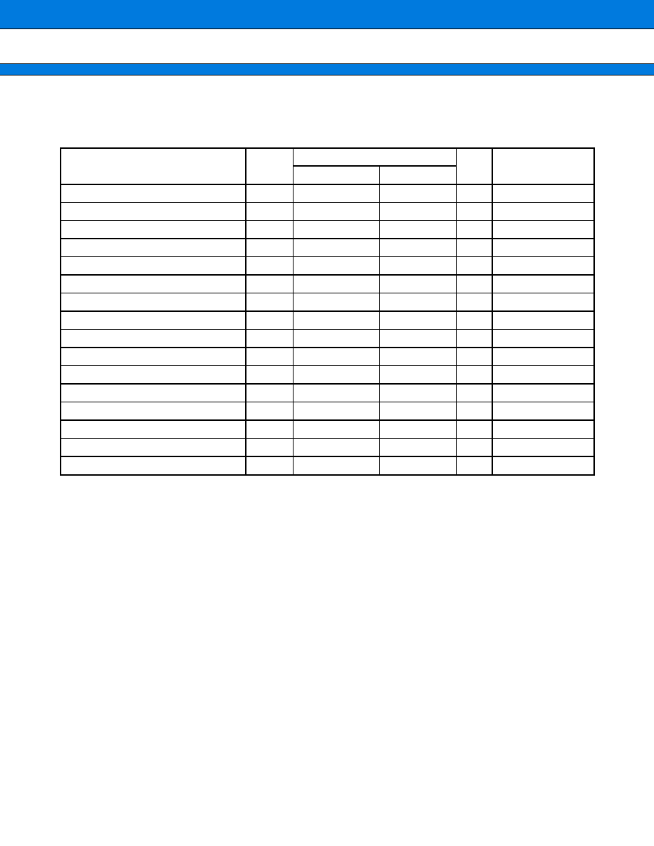
ELECTRICAL CHARACTERISTICS
1.
Absolute Maximum Ratings
(V
SS
=
AV
SS
=
0 V)
*1 : Care must be taken that AV
DD
and AV
RH
do not exceed V
DD
+
0.3 V such as when turning on the device.
Also care must be taken that AV
RH
does not exceed AV
DD
.
*2 : V
I
and V
O
may not exceed V
DD
+
0.3 V.
*3 : The maximum output current is the peak value for a single pin.
*4 : The average output current is the average current for a single pin over a period of 100 ms.
*5 : The total average output current is the average current for all pins over a period of 100 ms.
WARNING: Semiconductor devices can be permanently damaged by application of stress (voltage, current,
temperature, etc.) in excess of absolute maximum ratings. Do not exceed these ratings.
Parameter
Symbol
Rating
Unit
Remarks
Min
Max
Power supply voltage
V
DD
V
SS
-
0.3
V
SS
+
3.5
V
Analog power supply voltage
AV
DD
V
SS
-
0.3
V
SS
+
3.5
V
*1
Analog reference voltage
AV
RH
V
SS
-
0.3
V
SS
+
3.5
V
*1
Input voltage
V
I
V
SS
-
0.3
V
SS
+
3.5
V
*2
Output voltage
V
O
V
SS
-
0.3
V
SS
+
3.5
V
*2
"L" level maximum output current
I
OL
10
mA
*3
"L" level average output current
I
OLAV
8
mA
*4
"L" level total maximum output current
I
OL
100
mA
"L" level total average output current
I
OLAV
50
mA
*5
"H" level maximum output current
I
OH
-
10
mA
*3
"H" level average output current
I
OHAV
-
4
mA
*4
"H" level total maximum output current
I
OH
-
50
mA
"H" level total average output current
I
OHAV
-
20
mA
*5
Power consumption
P
D
500
mW
Operating temperature
T
A
-
20
+
70
°
C
Storage temperature
Tstg
-
55
+
150
°
C

MB
91191/192 Series
17
2.
Recommended Operating Conditions
(V
SS
=
AV
SS
=
0 V)
WARNING: The recommended operating conditions are required in order to ensure the normal operation of the
semiconductor device. All of the device's electrical characteristics are warranted when the device is
operated within these ranges.
Always use semiconductor devices within their recommended operating condition ranges. Operation
outside these ranges may adversely affect reliability and could result in device failure.
No warranty is made with respect to uses, operating conditions, or combinations not represented on
the data sheet. Users considering application outside the listed conditions are advised to contact their
FUJITSU representatives beforehand.
Parameter Symbol
Value
Unit
Remarks
Min
Max
Power supply voltage
V
DD
2.7
3.3
V
Normal operation
2.0
3.3
Maintaining RAM state in
stop mode
Analog power supply voltage
AV
DD
V
SS
-
0.3
V
DD
+
0.2
V
Analog reference voltage
AV
RH
AV
SS
AV
DD
V
Operating temperature
T
A
-
20
70
°
C

MB
91191/192 Series
18
3.
DC Characteristics
(V
DD
=
3.0 V
±
0.3 V, V
SS
=
AV
SS
=
0 V, T
A
=
-
20
°
C to
+
70
°
C)
*1 : X0, X1, OSCI, OSCO
*2 : RST, PC3 to PC1, PD6, PD5, PD3, PD2, PA7 to PA0, P12 to P10, P07 to P00, PD7, PD0
*3 : Inputs other than *1, *2, MD2 to MD0
*4 : P07 to P00, P17 to P10, P27 to P20, P47 to P40, P67 to P60, P70, P87 to P80, P94 to P90, PA7 to PA0,
PB7 to PB0, PC7 to PC2, PD7, PD6, PD3, PD0
*5 : P37 to P30, P57 to P50
*6 : PD5, PD4, PD2, PD1, PC1, PC0
*7 : Operating current for X0
=
20 MHz, OSCI
=
V
SS
(fixed) , all port outputs
=
low, gear selection : CPU
=
10 MHz,
peripherals
=
20 MHz
*8 : Operating current in sleep mode for X0
=
20 MHz, OSCI
=
V
SS
(fixed), all port outputs
=
low, gear selection :
CPU
=
10 MHz, peripherals
=
20 MHz
*9 : Operating current in stop mode for X0
=
20 MHz, OSCI
=
V
SS
(fixed) , all port outputs
=
low, gear selection :
CPU
=
10 MHz, peripherals
=
20 MHz
Parameter
Symbol
Pin Name
Condition
Value
Unit
Remarks
Min
Typ
Max
"H" level
input voltage
V
IH
*3
0.7 V
DD
V
DD
+
0.3
V
V
IHS
*1
V
DD
-
0.4
V
DD
+
0.3
V
*2
0.8 V
DD
V
DD
+
0.3
V
V
IHM
MD2 to MD0
V
DD
V
DD
+
0.3
V
"L" level
input
voltage
V
IL
*3
V
SS
-
0.3
0.2 V
DD
V
V
ILS
*1
V
SS
-
0.3
V
SS
+
0.4
V
*2
V
SS
-
0.3
0.2 V
DD
V
V
ILM
MD2 to MD0
V
SS
-
0.3
V
SS
V
"H" level
output
voltage
V
OH1
*4
V
DD
=
3.0 V,
I
OH
=
-
4.0 mA
2.4
V
MB91F191A
2.4
V
MB91191R
V
OH2
*5, *6
V
DD
=
3.0 V,
I
OH
=
-
8.0 mA
2.4
V
MB91F191A
2.4
V
MB91191R
"L" level
output
voltage
V
OL1
*4
V
DD
=
3.0 V,
I
OL
=
4.0 mA
0.6
V
V
OL2
*5, *6
V
DD
=
3.0 V,
I
OL
=
8.0 mA
0.6
V
V
OL3
*4, *5, *6
V
DD
=
3.0 V,
I
OL
=
1.0 mA
0.3
V
MB91191R
Input leak
current
I
LI1
*2
V
DD
=
3.0 V,
V
SS
<
V
I
<
V
DD
±
1
±
5
µ
A
I
LIX
X0, OSCI
±
8
±
20
µ
A
Power
supply
current
I
DD
V
DD
V
DD
=
3.0 V, *7
50.1
60
mA MB91F191A
16
25
mA MB91191R
I
DDS
V
DD
=
3.0 V, *8
24
36
mA MB91F191A
13
18
mA MB91191R
I
DDH
V
DD
=
3.0 V,
T
A
=
25
°
C, *9
1
240
µ
A
MB91F191A
10
300
µ
A
MB91191R
Input
capacitance
C
IN
Other than V
DD
, V
SS
,
AV
DD
, AV
SS
, and AV
RH
10
pF

MB
91191/192 Series
19
4.
AC Characteristics
(1) Clock Timings
(V
DD
=
3.0 V
±
0.3 V, V
SS
=
AV
SS
=
0 V, T
A
=
-
20
°
C to
+
70
°
C)
* : The frequency fluctuation value is the maximum percentage deviation from the preset center frequency when
using the multiplier (when PLL is locked) .
Parameter
Symbol
Condition
Value
Unit
Remarks
Min
Max
Clock frequency
f
C
10
20
MHz
Clock cycle time
t
C
50
100
ns
Frequency fluctuation* (PLL locked)
r
10
%
Input clock pulse width
P
WH
20
ns
P
WL
Input clock rise/fall time
t
CR
8
ns
t
CF
Internal operating clock
frequency
CPU
f
CP
When wait
controller set to
1 wait cycle
5
20
MHz
Peripherals
f
CPP
10
20
MHz
Internal operating clock
cycle time
CPU
t
CP
50
200
ns
Peripherals
t
CPP
50
100
ns
f
=
Center frequency f
0
+
-
+
-
|
|
f
0
×
100 (%)
t
c
P
WH
t
cf
P
WL
t
cr
Frequency (Hz)
Power supply voltage (V)
3.3
2.7
Guaranteed operation range
f
cp
f
cpp
10 M 20 M

MB
91191/192 Series
20
The figure below shows the relationship between the X0 input and the internal clock based on the GCR (Gear
Control Register) , CHC, CCK1, and CCK0 bit settings.
Where t
CYCH
is the H level width of the internal clock and t
CYCL
is the L level width.
For example, when set to source oscillation
×
1/2, gear
×
1/4 and X0 input frequency
=
20 MHz : t
CYC
=
400 ns,
t
CYCH
=
350 ns, t
CYCL
=
50 ns
CCK1/0:11
X0 input
Source oscillation
×
1
(CHC bit in GCR
=
0)
(a) gear
×
1
Internal clock
CCK1/0:00
t
CYC
t
CYC
t
CYC
t
CYC
t
CYC
t
CYC
t
CYC
t
CYC
(b) gear
×
1/2
Internal clock
Internal clock
Internal clock
CCK1/0:01
(c) gear
×
1/4
Internal clock
CCK1/0:10
(d) gear
×
1/8
CCK1/0:11
Source oscillation
×
1/2
(CHC bit in GCR
=
1)
(a) gear x 1
Internal clock
CCK1/0:00
(b) gear x 1/2
CCK1/0:01
(c) gear x 1/4
Internal clock
CCK1/0:10
(d) gear x 1/8
Internal clock
MB
91191/192 Series
21
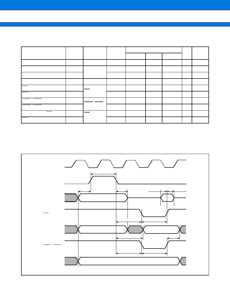
(2) Multiplex Bus Read/Write Operation
(V
DD
=
+
3.0 V
±
0.3 V, V
SS
=
AV
SS
=
0 V, T
A
=
-
20
°
C to
+
70
°
C)
*1 : When the bus is delayed by automatic wait insertion, add (t
CYC
×
number of wait cycles) to this value.
*2 : This value is for gear setting
=
×
1
For the value for gear settings 1/2, 1/4, and 1/8, substitute 1/2, 1/4, and 1/8 respectively for n in the formula below.
Formula : t
CYCH
=
(1
-
n
/
2)
×
t
CYC
t
CYCL
=
(n
/
2)
×
t
CYC
Parameter
Symbol
Pin Name
Condi-
tion
Value
Unit
Re-
marks
Min
Typ
Max
ALE pulse width
t
EHEL
ALE
t
CYC
-
10
ns
Address delay time
t
EHAV
A15 to A0
,
D31 to D16
t
CYCH
-
15
t
CYCH
t
CYCH
+
15
ns
*2
Address clear time
t
EHAX
t
CYCL
-
2
t
CYCL
t
CYCL
+
10
ns
*2
Data delay time
t
ELDV
D31 to D16
t
CYCL
+
26
ns
*2
RD delay time
t
ELRL
RD
t
CYC
-
11
t
CYC
t
CYC
+
11
ns
RD pulse width
t
RLRH
t
CYC
-
11
t
CYC
t
CYC
+
11
ns
*1
WR0, WR1 delay time
t
ELWL
WR0, WR1
t
CYC
-
11
t
CYC
t
CYC
+
11
ns
WR0, WR1 pulse width
t
WLWH
t
CYC
-
11
t
CYC
t
CYC
+
11
ns
*1
Data setup
RD
time
t
DSRH
RD
,
D31 to D16
15
ns
RD
Data hold time
t
RHDX
0
ns
t
WLWH
Internal
clock
ALE
Read time
D31 to D16
MPX bus
RD
Write time
D31 to D16
MPX bus
WR0 , WR1
A15 to A08
When not
multiplexed
t
EHEL
t
EHAV
t
ELAX
t
DSRH
t
RHDX
t
ELRL
t
RLRH
t
ELDV
t
WHDX
t
ELWL

MB
91191/192 Series
22
(3) Reset Input Ratings
(V
DD
=
3.0 V
±
0.3 V, V
SS
=
AV
SS
=
0 V, T
A
=
-
20
°
C to
+
70
°
C)
(4) Power-On Reset
(V
DD
=
3.0 V
±
0.3 V, V
SS
=
AV
SS
=
0 V, T
A
=
-
20
°
C to
+
70
°
C)
Parameter
Symbol
Pin Name
Value
Unit
Remarks
Min
Max
Reset input time
t
RSTL
RST
5 t
CP
ns
Paramete
Symbol
Pin Name
Value
Unit
Remarks
Min
Max
Power supply rise time
t
R
V
DD
20
ms
Power supply cutoff time
t
OFF
2
ms
0.2 V
DD
RST
t
RSTL
V
DD
t
R
2.7 V
0.2 V
t
OFF
When turning on the power, start with
the RST pin in the "L" level state and
allow a time of t
RSTL
after reaching
the V
DD
power supply level before
changing the pin to the "H" level.
V
DD
3.0 V
2.0 V
V
SS
V
DD
RST
Maintain RAM data
t
RSTL
Recommended rate of voltage
rise is 50 mV/ms or less.
Sudden changes in the power supply voltage may cause a power-on reset.
The recommended practice if you wish to change the power supply voltage while the device is operating
is to raise the voltage smoothly.

MB
91191/192 Series
23
(5) Serial I/O (CH0 to 2)
(V
DD
=
+
3.0 V
±
0.3 V, V
SS
=
AV
SS
=
0 V, T
A
=
-
20
°
C to
+
70
°
C)
Parameter
Sym-
bol
Condition
Value
Unit
Remarks
Min
Max
Serial clock cycle time
t
SCYC
Internal clock
8 t
CPP
ns
SCK
SO delay time
t
SLOV
-
10
50
ns
Valid SI
SCK
t
IVSH
50
ns
SCK
valid SI hold time
t
SHIX
50
ns
Serial clock "H" pulse width
t
SHSL
External clock
4 t
CPP
-
10
ns
Serial clock "L" pulse width
t
SLSH
4 t
CPP
-
10
ns
SCK
SO delay time
t
SLOV
0
50
ns
Valid SI
SCK
t
IVSH
50
ns
SCK
valid SI hold time
t
SHIX
50
ns
Serial busy time
t
BUSY
6 t
CPP
ns
SCS
SCK, SO delay time
t
CLZO
50
ns
SCS
SCK input mask time
t
CLSL
3 t
CPP
ns
SCS
SCK, SO Hi-Z time
t
CHOZ
50
ns
t
SCYC
SCK
t
SLOV
SO
SI
t
IVSH
t
SHIX
t
CLSL
t
CLZO
t
SLSH
t
SLOV
t
SHSL
t
BUSY
t
CHOZ
SCK
SO
SI
t
IVSH
t
SHIX
SCS
· Internal shift clock mode
· External shift clock mode

MB
91191/192 Series
24
(6) FG Pulse Input
(V
DD
=
3.0 V
±
0.3 V, V
SS
=
AV
SS
=
0 V, T
A
=
-
20
°
C to
+
70
°
C)
Note : t
C
is the clock cycle time of the X0 and X1 pin oscillation.
(7) Timer External Clock Input
(V
DD
=
+
3.0 V
±
0.3 V, V
SS
=
AV
SS
=
0 V, T
A
=
-
20
°
C to
+
70
°
C)
Parameter
Symbol
Pin Name
Value
Unit
Remarks
Min
Max
Servo input "H" pulse width
t
SPWH
CFG, DFG, DPG,
RFG0, RFG1,
EXI0 to EXI2
t
C
+
50
ns
Servo input "L" pulse width
t
SPWL
t
C
+
50
ns
Parameter
Symbol
Pin Name
Value
Unit
Remarks
Min
Max
Timer 4 input "H" pulse width
t
ECWH
EC4
4 t
C
+
50
ns
Timer 4 input "L" pulse width
t
ECWL
4 t
C
+
50
ns
Timer 5 input "H" pulse width
t
ECWH
EC5
4 t
CPP
ns
Timer 5 input "L" pulse width
t
ECWL
4 t
CPP
ns
CFG
DFG, DPG
RFG0, RFG1
EXI0 to EXI2
t
SPWH
t
f
t
SPWL
t
r
EC4,
EC5
t
r
t
ECWH
t
f
t
ECWL

MB
91191/192 Series
25
(8) General-Purpose Prescaler
(V
DD
=
3.0 V
±
0.3 V, V
SS
=
AV
SS
=
0 V, T
A
=
-
20
°
C to
+
70
°
C)
Parameter
Symbol
Pin Name
Value
Unit
Remarks
Min
Max
PCK input clock frequency
f
CP
PCK
12
MHz
PCK input "H" pulse width
t
SPWH
33
ns
PCK input "L" pulse width
t
SPWL
33
ns
PCK input
Fall time
t
f
PCK
100
ns
Rise time
t
r
PO output delay time
t
POPI
PO
80
ns
PCK
PO
t
SPWH
t
f
t
SPWL
t
r
t
POPI

MB
91191/192 Series
26
5.
Electrical Characteristics for the A/D Converter
(V
DD
=
3.0 V
+
0.3 V, V
SS
=
AV
SS
=
0 V, T
A
=
-
20
°
C to
+
70
°
C)
Notes :
·
The relative error increases as |AV
RH
| becomes smaller.
·
Ensure that the output impedance of the external circuit connected to the analog input meets the following
condition :
Output impedance of external circuit
<
7 k
(approx.)
If the output impedance of the external circuit is too high, the analog voltage sampling time may be too
short. (Sampling time
=
6.4
µ
s for a 20 MHz machine clock)
Parameter
Symbol
Pin
Name
Condition
Value
Unit Remarks
Min
Typ
Max
Resolution
10
bit
Conversion time
8.4
µ
s
Total error
V
DD
=
AV
DD
=
3.0 V,
AV
RH
=
3.0 V
±
4.0
LSB
Linearity error
±
3.5
LSB
Differential linearity error
±
2.0
LSB
Zero transition error
V
OT
AN-0 to
AN-F
V
DD
=
AV
DD
=
3.0 V,
AV
RH
=
3.0 V
AV
SS
-
1.5
AV
SS
+
0.5
AV
SS
+
2.5
LSB
Full-scale transition error
V
FST
AN-0 to
AN-F
AV
RH
-
5.5
AV
RH
-
1.5
AV
RH
+
0.5
LSB
Analog input current
I
AIN
AN-0 to
AN-F
0.1
10
µ
A
Analog input voltage
V
AIN
AN-0 to
AN-F
AV
SS
AV
RH
V
Reference voltage
AV
RH
AV
RH
AV
DD
V
Power
supply
current
During
conversion
I
A
AV
DD
V
DD
=
AV
DD
=
3.0 V
3.0
mA
Conver-
sion halted
I
AH
5.0
µ
A
Reference
voltage
supply
current
During
conversion
I
R
AV
RH
V
DD
=
AV
DD
=
3.0 V,
AV
RH
=
3.0 V
100
µ
A
Conver-
sion halted
I
RH
10
µ
A
Variation between
channels
AN-0 to
AN-F
4
LSB

MB
91191/192 Series
27
6.
Flash Memory Erase and Programming performance
Parameter
Condition
Value
Unit
Remarks
Min
Typ
Max
Sector erase time
T
A
=
+
25
°
C
,
V
CC
=
3.0 V
1
15
s
Excludes 00H programming prior
erasure
Chip erase time
10
s
MB91F191A Excludes 00H
programming prior
erasure
12
MB91F192
Half word
(16 bit width)
programming time
16
3,600
µ
s
Excludes system-level overhead
Erase/Program
cycle
10,000
cycle
Data holding time
100
,
000
h

MB
91191/192 Series
28
7.
A/D Converter Glossary
· Resolution : The change in analog voltage that can be recognized by the A/D converter.
· Linearity error
The deviation between the actual conversion characteristics and the line linking the zero transition point
("00 0000 0000
B
"
"00 0000 0001
B
") and the full scale transition point ("11 1111 1110
B
"
"11 1111
1111
B
") .
· Differential linearity error
The variation from the ideal input voltage required to change the output code by 1 LSB.
· Total error
The total error is the difference between the actual value and the theoretical value.
Includes the zero transition error, full-scale transition error and linearity error.
1 LSB' (Theoretical)
=
[V]
Total error for digital output N
=
V
OT
' (Theoretical)
=
AV
SS
+
0.5 LSB' [V]
V
FST
' (Theoretical)
=
AV
RH
-
1.5 LSB' [V]
V
NT
: Voltage at which digital output changes from (N
+
1) to N
AV
RH
-
AV
SS
1024
V
NT
-
{1 LSB'
×
(N
-
1)
+
0.5 LSB'}
1 LSB'
1.5 LSB'
Digital Output
3FF
3FE
3FD
004
003
002
001
AV
SS
0.5 LSB'
Theoretical characteristic
Actual conversion
characteristic
{1 LSB'
×
(N
-
1)
+
0.5 LSB'}
Actual conversion
characteristic
Total Error
AV
RH
Analog Input
V
NT
(Measured value)

MB
91191/192 Series
29
=
[LSB]
V
OT
' (Theoretical)
=
[V]
V
OT
: Voltage at which digital output changes from (000)
H
to (001)
H
.
V
FST
: Voltage at which digital output changes from (3FE)
H
to (3FF)
H
.
V
FST
-
V
OT
1022
=
-
1 LSB [LSB]
V
(N+1) T
-
V
NT
1 LSB'
Differential linearity error
for digital output N
V
NT
-
{1 LSB
×
(N
-
1)
+
V
OT
}
1 LSB'
Linearity error for
digital output N
Digital Output
Digital Output
Analog Input
Linearity Error
AV
SS
AV
RH
Analog Input
AV
SS
AV
RH
V
OT
(Measured value)
Theoretical characteristic
Actual conversion
characteristic
V
NT
(Measured
value)
{1 LSB
×
(N
-
1)
+
Vo
T
'}
Actual conversion characteristic
3FF
3FE
3FD
004
003
002
001
Differential Linearity Error
Actual conversion characteristic
V
NT
(Measured value)
Actual conversion characteristic
Theoretical characteristic
N
+
1
N
N
-
1
N
-
2
V
FST
(Measured
value)
V
FST
(Measured
value)

MB
91191/192 Series
30
s
s
s
s
ORDERING INFOMATION
Part No.
Package
Remarks
MB91191RPFF
MB91192PFF
MB91F191APFF
MB91F192PFF
Plastic LQFP, 120-pin
(FPT-120P-M05)
MB91192LGA
MB91F192LGA
Plastic FLGA, 144-pin
(LGA-144P-M02)

MB
91191/192 Series
31
s
s
s
s
PACKAGE DIMENSION
(Continued)
Plastic LQFP, 120-pin
(FPT-120P-M05)
Note 1) * : These dimensions do not include resin protrusion.
Note 2) Pins width and pins thickness include plating thickness.
Note 3) Pins width do not include tie bar cutting remainder.
Dimensions in mm (inches).
C
2003 FUJITSU LIMITED F120006S-c-4-5
0.07(.003)
M
INDEX
16.00±0.20(.630±.008)SQ
14.00±0.10(.551±.004)SQ
1
30
31
60
91
120
61
90
LEAD No.
(Stand off)
0.10±0.10
(.004±.004)
0.25(.010)
(.024±.006)
0.60±0.15
(.020±.008)
0.50±0.20
(Mounting height)
0~8
°
Details of "A" part
1.50
+0.20
0.10
+.008
.004
.059
"A"
0.40(.016)
0.16±0.03
(.006±.001)
0.145±0.055
(.006±.002)
0.08(.003)
*

MB
91191/192 Series
32
(Continued)
Plastic FLGA, 144-pin
(LGA-144P-M02)
Dimensions in mm (inches).
C
2001 FUJITSU LIMITED L144002S-c-1-1
11.00±0.10
0.08(.003)
0.65(.026)TYP
INDEX AREA
9.10±0.10
A
1
0.45(.018)
0.45(.018)
144-ř0.35
(.358±.004)
0.08(.003)
M
(144-ř.014)
(.433±.004)
(3-ř.018)
3-ř0.45
Max.
1.40(.055)
11.00±0.10(.433±.004)SQ
REF
5.175(.204)
2
3
4
5
6
7
8
9
10
11
12
13
14
15
B
C
D
E
F
G
H
J
K
L
M
N
P
R
5.175
(.204)

MB
91191/192 Series
FUJITSU LIMITED
All Rights Reserved.
The contents of this document are subject to change without notice.
Customers are advised to consult with FUJITSU sales
representatives before ordering.
The information, such as descriptions of function and application
circuit examples, in this document are presented solely for the
purpose of reference to show examples of operations and uses of
Fujitsu semiconductor device; Fujitsu does not warrant proper
operation of the device with respect to use based on such
information. When you develop equipment incorporating the
device based on such information, you must assume any
responsibility arising out of such use of the information. Fujitsu
assumes no liability for any damages whatsoever arising out of
the use of the information.
Any information in this document, including descriptions of
function and schematic diagrams, shall not be construed as license
of the use or exercise of any intellectual property right, such as
patent right or copyright, or any other right of Fujitsu or any third
party or does Fujitsu warrant non-infringement of any third-
partyĹfs intellectual property right or other right by using such
information. Fujitsu assumes no liability for any infringement of
the intellectual property rights or other rights of third parties which
would result from the use of information contained herein.
The products described in this document are designed, developed
and manufactured as contemplated for general use, including
without limitation, ordinary industrial use, general office use,
personal use, and household use, but are not designed, developed
and manufactured as contemplated (1) for use accompanying fatal
risks or dangers that, unless extremely high safety is secured, could
have a serious effect to the public, and could lead directly to death,
personal injury, severe physical damage or other loss (i.e., nuclear
reaction control in nuclear facility, aircraft flight control, air traffic
control, mass transport control, medical life support system, missile
launch control in weapon system), or (2) for use requiring
extremely high reliability (i.e., submersible repeater and artificial
satellite).
Please note that Fujitsu will not be liable against you and/or any
third party for any claims or damages arising in connection with
above-mentioned uses of the products.
Any semiconductor devices have an inherent chance of failure. You
must protect against injury, damage or loss from such failures by
incorporating safety design measures into your facility and
equipment such as redundancy, fire protection, and prevention of
over-current levels and other abnormal operating conditions.
If any products described in this document represent goods or
technologies subject to certain restrictions on export under the
Foreign Exchange and Foreign Trade Law of Japan, the prior
authorization by Japanese government will be required for export
of those products from Japan.
F0302
©
FUJITSU LIMITED Printed in Japan