
DS07-16306-3E
FUJITSU SEMICONDUCTOR
DATA SHEET
32-bit Proprietary Microcontrollers
CMOS
FR30 Family MB91150 Series
MB91F155A/MB91155/MB91154
s
s
s
s
DESCRIPTION
The MB91F155A/MB91155/MB91154 is a single-chip microcontroller using a RISC-CPU (FR 30 series) as its
core. It contains peripheral I/O resources suitable for audio, MD and so on which are required to operate at low
power consumption.
s
s
s
s
FEATURES
1.
CPU
· 32-bit RISC (FR30) , load/store architecture, 5-stage pipeline
· General-purpose registers : 32 bits
×
16
· 16-bit fixed-length instructions (basic instructions) , 1 instruction/ 1 cycle
· Memory-to-memory transfer, bit processing, barrel shift processing : Optimized for embedded applications
· Function entrance/exit instructions, and multiple load/store instructions of register contents, instruction systems
supporting high level languages
· Register interlock functions, efficient assembly language description
· Branch instructions with delay slots : Reduced overhead time in branching executions
· Internal multiplier/supported at instruction level
Signed 32-bit multiplication : 5 cycles
Signed 16-bit multiplication : 3 cycles
· Interrupt (PC and PS saving) : 6 cycles, 16 priority levels
(Continued)
s
s
s
s
PACKAGE
144-pin plastic LQFP
144-pin plastic LQFP
(FPT-144P-M08)
(FPT-144P-M01)

MB91F155A/MB91155/MB91154
2
2.
Bus Interface
· 16-bit address output, 8/16-bit data input and output
· Basic bus cycle : 2-clock cycle
· Support for interface for various types of memory
· Unused data/address pins can be configured us input/output ports
· Support for little endian mode
3.
Internal ROM
MB91F155A
FLASH products : 510 Kbytes
MB91155
Mask product : 510 Kbytes
MB91154
Mask product : 384 Kbytes
4.
Internal RAM
Mask, FLASH products : 2 Kbytes
5.
Internal Data RAM
MB91F155, MB91155
FLASH, Mask products : 32 Kbytes
MB91154
FLASH, Mask product : 20 Kbytes
6.
DMAC
DMAC in descriptor format for placing transfer parameters on to the main memory.
Capable of transferring a maximum of eight internal and external factors combined.
Three channels for external factors
7.
Bit Search Module
Searches in one cycle for the position of the bit that changes from the MSB in one word to the initial I/O.
8.
Timers
· 16-bit OCU
×
8 channels, ICU
×
4 channels, Free-run timer
×
1 channel
· 8/16-bit up/down timer/counter (8-bit
×
2 channels or 16-bit
×
1 channel)
· 16-bit PPG timer
×
6 channels. The output pulse cycle and duty can be varied as desired
· 16-bit reload timer
×
4 channels
9.
D/A Converter
· 8-bit
×
3 channels
10. A/D Converter (Sequential Comparison Type)
· 10-bit
×
8 channels
· Sequential conversion method (conversion time : 5.0
µ
s@33 MHz)
· Single conversion or scan conversion can be selected, and one-shot or continuous or stop conversion mode
can be set respectively.
· Conversion starting function by hardware/software.
(Continued)

MB91F155A/MB91155/MB91154
3
(Continued)
11. Serial I/O
· UART
×
4 channels. Any of them is capable of serial transfer in sync with clock attached with the LSB/MSB
switching function.
· Serial data output and serial clock output are selectable by push-pull/open drain software.
· A 16-bit timer (U-timer) is contained as a dedicated baud rate generator allowing any baud rate to be generated.
12. I
2
C Bus Interface
· One channel master/slave send and receive
· Arbitration and clock synchronization functions
(The product is licensed with the Philips I
2
C patent to support those customers who intend to use this product
in an I
2
C system in compliance with the standard I
2
C specification stipulated by Philips.)
13. Clock Switching Function
· Gear function : Operating clock ratios to the basic clock can be set independently for the CPU and peripherals
from four types, 1 : 1, 1 : 2, 1 : 4 or 1 : 8.
14. Clock Function (Calendar Macro)
· Internal 32 kHz clock function
· It is possible to perform the clock function (oscillation frequency: 32 kHz) even in a stop mode. (The oscillation
does not suspend during a stop mode.)
15. Interrupt Controller
External interrupt input (16 channels in total) :
· Allows the rising edge/falling edge/H level/L level to be set.
Internal interrupt factors :
· Interrupt by resources and delay interrupt
16. Others
· Reset cause : Power on reset/watchdog timer/software reset/external reset
· Low power consumption mode : Sleep/stop
· Package : 144-pin LQFP
· CMOS technology (0.35
µ
m)
· Power supply voltage : 3.15 V to 3.6 V
· MB91F155 is to be MB91F155A.
MB91F155A/MB91155/MB91154
4
s
s
s
s
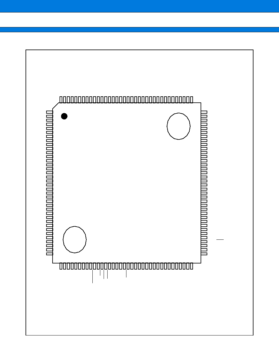
PIN ASSIGNMENT
(TOP VIEW)
(FPT-144P-M08)
(FPT-144P-M01 : MB91F155A only)
P20/D16
P21/D17
P22/D18
P23/D19
P24/D20
P25/D21
P26/D22
P27/D23
V
SS
P30/D24
P31/D25
P32/D26
P33/D27
P34/D28
P35/D29
P36/D30
P37/D31
P40/A00
P41/A01
P42/A02
P43/A03
P44/A04
P45/A05
P46/A06
P47/A07
V
SS
V
CC
P50/A08
P51/A09
P52/A10
P53/A11
P54/A12
P55/A13
P56/A14
P57/A15
P60/A16
1
2
3
4
5
6
7
8
9
10
11
12
13
14
15
16
17
18
19
20
21
22
23
24
25
26
27
28
29
30
31
32
33
34
35
36
P61/A17
P62/A18
P63/A19
P64/A20
P65/A21
P66/A22
P67/A23
V
SS
P80/RDY
P81/BGRNT
P82/BRQ
P83/RD
P84/WR0
P85/WR1
P86/CLK
MD2
MD1
MD0
RST
V
CC
X1
X0
V
SS
PC0/INT0
PC1/INT1
PC2/INT2
PC3/INT3
PC4/INT4/CS0
PC5/INT5/CS1
PC6/INT6/CS2
PC7/INT7/CS3
V
CC
PD0/AIN0/INT8/TRG0
PD1/BIN0/INT9/TRG1
PD2/AIN1/INT10/TRG2
PD3/BIN1/INT11/TRG3
37
38
39
40
41
42
43
44
45
46
47
48
49
50
51
52
53
54
55
56
57
58
59
60
61
62
63
64
65
66
67
68
69
70
71
72
108
107
106
105
104
103
102
101
100
99
98
97
96
95
94
93
92
91
90
89
88
87
86
85
84
83
82
81
80
79
78
77
76
75
74
73
PH5/SCK1/TO1
PI0/SIN2
PI1/SOT2
PI2/SCK2/TO2
PI3/SIN3
PI4/SOT3
PI5/SCK3/TO3
V
SS
PJ0/SCL
PJ1/SDA
V
SS
V
CC
PG5/PPG5
PG4/PPG4
PG3/PPG3
PG2/PPG2
PG1/PPG1
PG0/PPG0
PF4
PF3/IN3
PF2/IN2
PF1/IN1
PF0/IN0
PE7/OC7
PE6/OC6
PE5/OC5
PE4/OC4
PE3/OC3
PE2/OC2
PE1/OC1
PE0/OC0
V
CC
PD7/ATG/INT15
PD6/DEOP2/INT14
PD5/ZIN1/INT13/TRG5
PD4/ZIN0/INT12/TRG4
144
143
142
141
140
139
138
137
136
135
134
133
132
131
130
129
128
127
126
125
124
123
122
121
120
119
118
117
116
115
114
113
112
111
110
109
V
SS
X1A
X0A
TEST
V
CC
PK7/AN7
PK6/AN6
PK5/AN5
PK4/AN4
PK3/AN3
PK2/AN2
PK1/AN1
PK0/AN0
AV
SS
AVRL
AVRH
AV
CC
DAVC
DAVS
DA0
DA1
DA2
V
CC
PL7/DACK2
PL6/DREQ2
PL5/DEOP1
PL4/DACK1
PL3/DREQ1
PL2/DEOP0
PL1/DACK0
PL0/DREQ0
PH0/SIN0
PH1/SOT0
PH2/SCK0/TO0
PH3/SIN1
PH4/SOT1

MB91F155A/MB91155/MB91154
5
s
s
s
s
PIN DESCRIPTION
(Continued)
Pin No.
Pin name
Circuit
type
Function
1
2
3
4
5
6
7
8
D16/P20
D17/P21
D18/P22
D19/P23
D20/P24
D21/P25
D22/P26
D23/P27
C
Bit 16 to bit 23 of external data bus
These pins are enabled only in 16-bit external bus mode.
These pins are available as ports in single-chip and 8-bit external bus
modes.
10
11
12
13
14
15
16
17
D24/P30
D25/P31
D26/P32
D27/P33
D28P34
D29/P35
D30/P36
D31/P37
C
Bit 24 to bit 31 of external data bus
These pins are available as ports in single-chip mode.
18
19
20
21
22
23
24
25
28
29
30
31
32
33
34
35
A00/P40
A01/P41
A02/P42
A03/P43
A04/P44
A05/P45
A06/P46
A07/P47
A08/P50
A09/P51
A10/P52
A11/P53
A12/P54
A13/P55
A14/P56
A15/P57
F
Bit 0 to bit 15 of external address bus
These pins are enabled in external bus mode.
These pins are available as ports in single-chip mode.
36
37
38
39
40
41
42
43
A16/P60
A17/P61
A18/P62
A19/P63
A20/P64
A21/P65
A22/P66
A23/P67
O
Bit 16 to bit 23 of external address bus
These pins are available as ports when the address bus is not in use.
45
RDY/P80
C
External RDY input
This function is enabled when external RDY input is allowed.
Input "0" when the bus cycle being executed does not end.
This pin is available as a port when external RDY input is not in use.

MB91F155A/MB91155/MB91154
6
(Continued)
Pin No.
Pin name
Circuit
type
Function
46
BGRNT/P81
F
External bus release acceptance output
This function is enabled when external bus release acceptance output is
allowed.
Output "L" upon releasing of the external bus.
This pin is available as a port when external bus release acceptance out-
put is not allowed.
47
BRQ/P82
C
External bus release request input
This function is enabled when external bus release request input is al-
lowed.
Input "1" when the release of the external bus is desired.
This pin is available as a port when external bus release request input is
not in use.
48
RD/P83
F
External bus read strobe output
This function is enabled when external bus read strobe output is allowed.
This pin is available as a port when external bus read strobe output is not
allowed.
49
WR0/P84
F
External bus write strobe output
This function is enabled in external bus mode.
This pin is available as a port in single chip mode.
50
WR1/P85
F
External bus write strobe output
This function is enabled in external bus mode when the bus width is 16
bits.
This pin is available as a port in single chip mode or when the external bus
width is 8 bits.
51
CLK/P86
F
System clock output
The pin outputs the same clock as the external bus operating frequency.
The pin is available as a port when it is not used to output the clock.
52
53
54
MD2
MD1
MD0
G
Mode pins
To use these pins, connect them directly to either V
CC
or V
SS
.
Use these pins to set the basic MCU operating mode.
55
RST
B
External reset input
57
58
X1
X0
A
High-speed clock oscillation pins (16.5 MHz)
60
61
62
63
INT0/PC0
INT1/PC1
INT2/PC2
INT3/PC3
H
External interrupt request input 0-3
Since this input is used more or less continuously when the corresponding
external interrupt is allowed, output by the port needs to be stopped ex-
cept when it is performed deliberately.
Since this port is allowed to input also in standby mode, it can be used to
reset the standby state.
These pins are available as ports when external interrupt request input is
not in use.

MB91F155A/MB91155/MB91154
7
(Continued)
Pin No.
Pin name
Circuit
type
Function
64
65
66
67
INT4/PC4/CS0
INT5/PC5/CS1
INT6/PC6/CS2
INT7/PC7/CS3
H
These pins also serve as the chip select output and external inter-
rupt request input 4-7.
When the chip select output is not allowed, these pins are available
as external interrupt requests or ports.
Since this input is used more or less continuously when the corre-
sponding external interrupt is allowed, output by the port needs to
be stopped except when it is performed deliberately.
Since this port is also allowed to input in standby mode, the port can
be used to reset the standby state.
These pins are available as ports when external interrupt request
input and chip select output are not in use.
69
70
71
72
73
74
PD0/AIN0/INT8/TRG0
PD1/BIN0/INT9/TRG1
PD2/AIN1/INT10/TRG2
PD3/BIN1/INT11/TRG3
PD4/ZIN0/INT12/TRG4
PD5/ZIN1/INT13/TRG5
H
External interrupt request input 8-13
Since this input is used more or less continuously when the corre-
sponding external interrupt is allowed, output by the port needs to
be stopped except when it is performed deliberately.
[AIN, BIN] Up/down timer input.
[TRG] PPG external trigger input.
Since this input is used more or less continuously while input is al-
lowed, output by the port needs to be stopped except when it is per-
formed deliberately.
These pins are available as ports when the external interrupt re-
quest input, up timer counter input, and PPG external trigger input
are not in use.
75
PD6/DEOP2/INT14
H
External interrupt request input 14
Since this input is used more or less continuously when the corre-
sponding external interrupt is allowed, output by the port needs to
be stopped except when it is performed deliberately.
[DEOP2] DMA external transfer end output.
This function is enabled when DMAC external transfer end output
is allowed.
This pin is available as a port when it is not in use as the external
interrupt request input or DMA external transfer end output.
76
PD7/ATG/INT15
H
External interrupt request input 15
Since this input is used more or less continuously when the corre-
sponding external interrupt is allowed, output by the port needs to
be stopped except when it is performed deliberately.
[ATG] A/D converter external trigger input.
Since this input is used more or less continuously when selected as
an A/D activation factor, output by the port needs to be stopped ex-
cept when it is performed deliberately.
This pin is available as a port when it is not in use as the external
interrupt request input or A/D converter external trigger input.

MB91F155A/MB91155/MB91154
8
(Continued)
Pin No.
Pin name
Circuit
type
Function
78
79
80
81
82
83
84
85
PE0/OC0
PE1/OC1
PE2/OC2
PE3/OC3
PE4/OC4
PE5/OC5
PE6/OC6
PE7/OC7
F
Output compare output
These pins are available as ports when output compare output is not al-
lowed.
86
87
88
89
PF0/IN0
PF1/IN1
PF2/IN2
PF3/IN3
F
Input capture input
This function is enabled when the input capture operation is input.
These pins are available as ports when input capture input is not in use.
90
PF4
F
General purpose I/O port
91
92
93
94
95
96
PG0/PPG0
PG1/PPG1
PG2/PPG2
PG3/PPG3
PG4/PPG4
PG5/PPG5
F
PPG timer output
This function is enabled when PPG timer output is allowed.
These pins are available as ports when PPG timer output is not allowed.
99
PJ1/SDA
Q
I
2
C interface I/O pin
This function is enabled when the I
2
C interface is allowed to operate.
While the I
2
C interface is in operation, keep the port output set to Hi-Z.
This pin is available as a port when the I
2
C interface is not in use.
100
PJ0/SCL
Q
I
2
C interface I/O pin
This function is enabled when the I
2
C interface is allowed to operate.
While the I
2
C interface is in operation, keep the port output set to Hi-Z.
This pin is available as a port when the I
2
C interface is not in use.
102
PI5/SCK3/TO3
P
UART3 clock I/O, Reload timer 3 output
When UART3 clock output is not allowed, reload timer 3 can be output by
allowing it.
This pin is available as a port when neither UART3 clock output nor reload
timer output is allowed.
103
PI4/SOT3
P
UART3 data output
This function is enabled when UART3 data output is allowed.
This pin is available as a port when UART3 clock output is not allowed.
104
PI3/SIN3
P
UART3 data input
Since this input is used more or less continuously while UART3 is en-
gaged in input operations, output by the port needs to be stopped except
when it is performed deliberately.
This pin is available as a port when UART3 output data input is not in use.

MB91F155A/MB91155/MB91154
9
(Continued)
Pin No.
Pin name
Circuit
type
Function
105
PI2/SCK2/TO2
P
UART2 clock I/O, Reload timer 2 output
When UART2 clock output is not allowed, reload timer 2 can be output by
allowing it.
This pin is available as a port when neither UART2 clock output nor reload
timer output is allowed.
106
PI1/SOT2
P
UART2 data output
This function is enabled when UART2 data output is allowed.
This pin is available as a port when UART2 clock output is not allowed.
107
PI0/SIN2
P
UART2 data input
Since this input is used more or less continuously while UART2 is en-
gaged in input operations, output by the port needs to be stopped except
when it is performed deliberately.
This pin is available as a port when UART2 data input is not in use.
108
PH5/SCK1/TO1
P
UART1 clock I/O, Reload timer 1 output
When UART1 clock output is not allowed, reload timer 1 can be output by
allowing it.
This pin is available as a port when neither UART1 clock output nor reload
timer output is allowed.
109
PH4/SOT1
P
UART1 data output
This function is enabled when UART1 data output is allowed.
This pin is available as a port when UART1 clock output is not allowed.
110
PH3/SIN1
P
UART1 data input
Since this input is used more or less continuously while UART1 is en-
gaged in input operations, output by the port needs to be stopped except
when it is performed deliberately.
This pin is available as a port when UART1 data input is not in use.
111
PH2/SCK0/TO0
P
UART0 clock I/O, Reload timer 0 output
When UART0 clock output is not allowed, reload timer 0 can be output by
allowing it.
This pin is available as a port when neither UART0 clock output nor reload
timer output is allowed.
112
PH1/SOT0
P
UART0 data output
This function is enabled when UART0 data output is allowed.
This pin is available as a port when UART0 clock output is not allowed.
113
PH0/SIN0
P
UART0 data input
Since this input is used more or less continuously while UART0 is en-
gaged in input operations, output by the port needs to be stopped except
when it is performed deliberately.
This pin is available as a port when UART0 data input is not in use.
114
DREQ0/PL0
F
DMA external transfer request input
Since this input is used more or less continuously when selected as a
DMAC transfer factor, output by the port needs to be stopped except when
it is performed deliberately.
This pin is available as a port when DMA external transfer request input is
not in use.

MB91F155A/MB91155/MB91154
10
(Continued)
Pin No.
Pin name
Circuit
type
Function
115
DACK0/PL1
F
DMA external transfer request acceptance output
This function is enabled when the DMAC external transfer request accep-
tance is allowed to be output.
This pin is available as a port when the DMAC transfer request accep-
tance is not allowed to be output.
116
DEOP0/PL2
F
DMA external transfer end output
This function is enabled when the end of DMAC external transfer is al-
lowed to be output.
117
DREQ1/PL3
F
DMA external transfer request input
Since this input is used more or less continuously when selected as a
DMAC transfer factor, output by the port needs to be stopped except when
it is performed deliberately.
This pin is available as a port when DMA external transfer request input is
not in use.
118
DACK1/PL4
F
DMA external transfer request acceptance output
This function is enabled when the DMAC external transfer request accep-
tance is allowed to be output.
This pin is available as a port when DMAC transfer request acceptance
output is not allowed.
119
DEOP1/PL5
F
DMA external transfer end output
This function is enabled when the end of DMAC external transfer is al-
lowed to be output.
120
DREQ2/PL6
F
DMA external transfer request input
Since this input is used more or less continuously when selected as a
DMAC transfer factor, output by the port needs to be stopped except when
it is performed deliberately.
This pin is available as a port when DMA external transfer request input is
not in use.
121
DACK2/PL7
F
DMA external transfer request acceptance output
This function is enabled when the DMAC external transfer request accep-
tance is allowed to be output.
This pin is available as a port when DMAC transfer request acceptance
output is not allowed.
123
124
125
DA2
DA1
DA0
D/A converter output
This function is enabled when D/A converter output is allowed.
126
DAVS
Power supply pin for the D/A converter
127
DAVC
Power supply pin for the D/A converter
128
AV
CC
Vcc power supply for the A/D converter
129
AVRH
A/D converter reference voltage (high potential side)
Be sure to turn on/off this pin with potential higher than AVRH applied to
V
CC
.
130
AVRL
A/D converter reference voltage (low potential side)
131
AV
SS
V
SS
power supply for the A/D converter

MB91F155A/MB91155/MB91154
11
(Continued)
Note : On the majority of pins listed above, the I/O port and the resource I/O are multiplexed, such as XXXX/Pxx.
When the port and the resource output compete against each other on these pins, priority is given to the
resource.
Pin No.
Pin name
Circuit
type
Function
132
133
134
135
136
137
138
139
AN0/PK0
AN1/PK1
AN2/PK2
AN3/PK3
AN4/PK4
AN5/PK5
AN6/PK6
AN7/PK7
N
A/D converter analog input
These pins are enabled when the AIC register is designated for analog
input.
These pins are available as ports when A/D converter analog input is
not in use.
141
TEST
G
The TEST pin must be connected to the power supply (V
CC
)
142
143
X0A
X1A
K
Low-speed clock (32 kHz) oscillation pin
27, 56, 68,
77, 97,
122, 140
V
CC
Power supply pin (V
CC
) for digital circuit
Always power supply pin (V
CC
) must be connected to the power
supply
9, 26, 44,
59, 98,
101, 144
V
SS
Earth level (V
SS
) for digital circuit
Always power supply pin (V
SS
) must be connected to the power
supply

MB91F155A/MB91155/MB91154
12
s
s
s
s
I/O CIRCUIT TYPE
(Continued)
Type
Circuit
Remarks
A
· High-speed oscillation circuit
(16.5 MHz)
Oscillation feedback resistor
=
approx. 1 M
B
· CMOS hysteresis input pin
CMOS hysteresis input
(standby control not attached)
Pullup resistor
C
· CMOS level I/O pin
CMOS level output
CMOS level input
(attached with standby control)
I
OL
=
4 mA
F
· CMOS hysteresis I/O pin
CMOS level output
CMOS hysteresis input
(attached with standby control)
I
OL
=
4 mA
X1
X0
Xout
Standby control signal
Digital input
Pout
Nout
CMOS input
Standby control
R
Pout
Nout
Hysteresis input
Standby control
R

MB91F155A/MB91155/MB91154
13
(Continued)
Type
Circuit
Remarks
G
· CMOS level input pin
CMOS level input
(standby control not attached)
H
· CMOS hysteresis I/O pin with pul-
lup control
CMOS level output
CMOS level input
(standby control not attached)
Pullup resistance
=
approx. 50 k
(Typ.)
I
OL
=
4 mA
K
· Clock oscillation circuit (32 kHz)
N
· Analog/CMOS level I/O pin.
CMOS level output
CMOS level input
(attached with standby control)
Analog input (Analog input is en-
abled when AIC's corresponding
bit is set to "1.")
I
OL
=
4 mA
R
Digital input
R
R
Pout
Pullup control
Hysteresis input
Nout
X1A
X0A
Xout
Pout
Nout
CMOS input
Standby control
Analog input
R

MB91F155A/MB91155/MB91154
14
(Continued)
Type
Circuit
Remarks
O
· CMOS hysteresis I/O pin
with pullup control
CMOS level output
CMOS hysteresis input
(attached with standby control)
Pullup resistance
=
approx. 50 k
(Typ.)
I
OL
=
4 mA
P
· CMOS hysteresis I/O pin
with pullup control.
CMOS level output
(attached with open drain con-
trol)
CMOS hysteresis input
(attached with standby control)
Pullup resistance
=
approx. 50 k
(Typ.)
I
OL
=
4 mA
Q
· Open drain I/O pin
· 5 V tolerance of voltage
· CMOS hysteresis input
(attached with standby control)
I
OL
=
15 mA
Pout
Pullup control
Hysteresis input
Standby control
Nout
R
R
Nout
Pullup control
Open drain control
Hysteresis input
Standby control
R
R
Nout
Hysteresis input
Standby control
R

MB91F155A/MB91155/MB91154
15
s
s
s
s
HANDLING DEVICES
1.
Preventing Latchup
In CMOS ICs, applying voltage higher than V
CC
or lower than V
SS
to input/output pin or applying voltage over
rating across V
CC
and V
SS
may cause latchup.
This phenomenon rapidly increases the power supply current, which may result in thermal breakdown of the
device. Make sure to prevent the voltage from exceeding the maximum rating.
2.
Treatment of Pins
· Treatment of unused pins
Unused pins left open may cause malfunctions. Make sure to connect them to pull-up or pull-down resistors.
· Treatment of open pins
Be sure to use open pins in open state.
· Treatment of output pins
Shortcircuiting an output pin with the power supply or with another output pin or connecting a large-capacity
load may causes a flow of large current. If this conditions continues for a lengthy period of time, the device
deteriorates. Take great care not to exceed the absolute maximum ratings.
· Mode pins (MD0-MD2)
These pins should be used directly connected to either V
CC
or V
SS
. In order to prevent noise from causing
accidental entry into test mode, keep the pattern length as short as possible between each mode pin and V
CC
or V
SS
on the board and connect them with low impedance.
· Power supply pins
When there are several V
CC
and V
SS
pins, each of them is equipotentially connected to its counterpart inside
of the device, minimizing the risk of malfunctions such as latch up. To further reduce the risk of malfunctions,
to prevent EMI radiation, to prevent strobe signal malfunction resulting from creeping-up of ground level and
to observe the total output current standard, connect all V
CC
and V
SS
pins to the power supply or GND.
It is preferred to connect V
CC
and V
SS
of MB91F155/MB91154 to power supply with minimal impedance possible.
It is also recommended to connect a ceramic capacitor as a bypass capacitor of about 0.1
µ
F between V
CC
and
V
SS
at a position as close as possible to MB91F155/MB91154.
· Crystal oscillator circuit
Noises around X0, X1, X0A, and X1A pins may cause malfunctions of MB91F155/MB91154. In designing the
PC board, layout X0, X1 (X0A, X1A) and crystal oscillator (or ceramic oscillator) and bypass capacitor for
grounding as close as possible.
It is strongly recommended to design PC board so that X0, X1, X0A, and X1A pins are surrounded by grounding
area for stable operation.
The MB91F155A, MB91155 and MB91154 devices do not contain a feedback resistor. To use the clock function,
you need to connect an external resistor.
3.
Precautions
· External Reset Input
It takes at least 5 machine cycle to input "L" level to the RST pin and to ensure inner reset operation properly.
· External Clocks
When using an external clock, normally, a clock of which the phase is opposite to that of X0 must be supplied
to the X0 and X1 pins simultaneously. However, when using the clock along with STOP (oscillation stopped)
X0A
X1A
MB91F155A/MB91155/MB91154

MB91F155A/MB91155/MB91154
16
mode, the X1 pin stops when "H" is input in STOP mode. To prevent one output from competing against another,
an external resistor of about 1 k
should be provided.
The following figure shows an example usage of an external clock.
Figure 2.1 An example usage of an external clock
4.
Care During Powering Up
· When powering up
When turning on the power supply, never fail to start from setting the RST pin to "L" level. And after the power
supply voltage goes to V
CC
level, at least after ensuring the time for 5 machine cycle, then set to "H" level.
· Source oscillation input
At turning on the power supply, never fail to input the clock before cancellation of the oscillation stabilizing
waiting.
· Power on resetting
When powering up or when turning the power back on after the supply voltage drops below the operation
assurance range, be sure to reset the power.
· Power on sequence
Turn on the power in the order of V
CC
, AV
CC
and AVRH. The power should be disconnected in inverse order.
· Even when an AD converter is not in use, connect AV
CC
to the V
CC
level and AV
SS
to the V
SS
level.
· Even when a DA converter is not in use, connect DAVC to the V
CC
level and DAVS to the V
SS
level.
5.
When the Clock Function (Calendar Macro) Is Not in Use
Not using the clock function, the clock oscillation pin must be configured as shown below.
X0
X1
MB91F155A/MB91155/MB91154
X0A
X1A
MB91F155A/MB91155/MB91154
OPEN
This product type does not allow the clock crystal oscillator to be stopped with software.

MB91F155A/MB91155/MB91154
17
s
s
s
s
BLOCK DIAGRAM
· MB91F155A, MB91155
FR30 CPU Core
I - Bus
D - Bus
I - Bus
D - Bus
C - Bus
External
Bus CTL
UART 4 ch
UTIMER 4 ch
16 bit
Reload Timer
RAM
2 KB
ROM
510 KB
Clock
Control
Interrupt
Controller
8 bit
Up/Down
Counter
External
Interrupt
2 ch
1 ch
4 ch
16 bit
Free RUN Timer
1 ch
16 bit
Input Capture
4 ch
16 bit
Output Compare
10 bit 8 input
A/D converter
8 bit 3 output
D/A converter
I
2
C Interface
8 ch
16 bit PPG
6 ch
16 ch
Calendar
Data RAM
DMAC 8 ch
Bit Search
32 KB
D - Bus
R - Bus
P
O
R
T
D
8
( )
P
O
R
T
L
8
( )
P
O
R
T
6
/
5
/
4
24
P
O
R
T
3
/
2
16
M
O
D
E
4
( )
(
)
(
)
P
O
R
T
8
7( )
P
O
R
T
C
8
( )
PD7/INT15/ATG (I)
PD6/INT14/DEOP2
PD5/INT13/ZIN1
PD4/INT12/ZIN0
PD3/INT11/BIN1
PD2/INT10/AIN1
PD1/INT9/BIN0 (I)
PD0/INT8/AIN0 (I)
PC7/INT7/CS3
PC6/INT6/CS2
PC5/INT5/CS1
PC4/INT4/CS0
PC3/INT3
PC2/INT2
PC1/INT1
PC0/INT0 (I)
A/D
DMAC
Up/Down
Counter
External
Interrupt
OSC
(2)
OSC
(2)
P
O
R
T
K
8
P
O
R
T
E
8
P
O
R
T
I
6
P
O
R
T
F
5
P
O
R
T
J
2
D
A
3
( )
( )
( )
P
O
R
T
H
6( )
P
O
R
T
G
6( )
( )
( )
( )
PE7/OC7
PE6/OC6
PE5/OC5
PE4/OC4
PE3/OC3
PE2/OC2
PE1/OC1
PE0/OC0
PL7/DACK2
PL6/DREQ2
PL5/DEOP1
PL4/DACK1
PL3/DREQ1
PL2/DEOP0 (O)
PL1/DACK0 (O)
PL0/DREQ0 (I)
P86/CLK (O)
P85/WR1 (O)
P84/WR0
P83/RD (O)
P82/BRQ (I)
P81/BGRNT (O)
P80/RDY (I)
P67/A23 (O)
P60/A16
P57/A15
P50/A8
P47/A7
P40/A0
P37/D31 (IO)
P30/D24
P27/D23
P20/D16
PG5/PPG5
PG4/PPG4
PG3/PPG3
PG2/PPG2
PG1/PPG1
PG0/PPG0
PF4
PF3/IN3
PF2/IN2
PF1/IN1
PF0/IN0
DA2
DA1
DA0
X0A
X1A
X0 (I)
X1 (I)
PH0/SIN0
PH1/SOT0
PH2/SCK0/TO0
PH3/SIN1
PH4/SOT1
PH5/SCK1/TO1
PI0/SIN2
PI1/SOT2
PI2/SCK2/TO2
PI3/SIN3
PI4/SOT3
PI5/SCK3/TO3
PK0/AN0
PK1/AN1
PK2/AN2
PK3/AN3
PK4/AN4
PK5/AN5
PK6/AN6
PK7/AN7
PJ0/SCL
PJ1/SDA
UART
TOX:
Reload
Timer
PPG
Input
Capture
Clock
Clock
DMAC
Bus
Control
Address
DATA
Output
Compare
A/D
I
2
C
MD1
MD2
RST
MD0

MB91F155A/MB91155/MB91154
18
· MB91154
FR30 CPU Core
I - Bus
D - Bus
I - Bus
D - Bus
C - Bus
External
Bus CTL
UART 4 ch
UTIMER 4 ch
16 bit
Reload Timer
RAM
2 KB
ROM
384 KB
Clock
Control
Interrupt
Controller
8 bit
Up/Down
Counter
External
Interrupt
2 ch
1 ch
4 ch
16 bit
Free RUN Timer
1 ch
16 bit
Input Capture
4 ch
16 bit
Output Compare
10 bit 8 input
A/D converter
8 bit 3 output
D/A converter
I
2
C Interface
8 ch
16 bit PPG
6 ch
16 ch
Calendar
Data RAM
DMAC 8 ch
Bit Search
20 KB
D - Bus
R - Bus
P
O
R
T
D
8
( )
P
O
R
T
L
8
( )
P
O
R
T
6
/
5
/
4
24
P
O
R
T
3
/
2
16
M
O
D
E
4
( )
(
)
(
)
P
O
R
T
8
7( )
P
O
R
T
C
8
( )
PD7/INT15/ATG (I)
PD6/INT14/DEOP2
PD5/INT13/ZIN1
PD4/INT12/ZIN0
PD3/INT11/BIN1
PD2/INT10/AIN1
PD1/INT9/BIN0 (I)
PD0/INT8/AIN0 (I)
PC7/INT7/CS3
PC6/INT6/CS2
PC5/INT5/CS1
PC4/INT4/CS0
PC3/INT3
PC2/INT2
PC1/INT1
PC0/INT0 (I)
A/D
DMAC
Up/Down
Counter
External
Interrupt
OSC
(2)
OSC
(2)
P
O
R
T
K
8
P
O
R
T
E
8
P
O
R
T
I
6
P
O
R
T
F
5
P
O
R
T
J
2
D
A
3
( )
( )
( )
P
O
R
T
H
6( )
P
O
R
T
G
6( )
(
)
( )
( )
PE7/OC7
PE6/OC6
PE5/OC5
PE4/OC4
PE3/OC3
PE2/OC2
PE1/OC1
PE0/OC0
PL7/DACK2
PL6/DREQ2
PL5/DEOP1
PL4/DACK1
PL3/DREQ1
PL2/DEOP0 (O)
PL1/DACK0 (O)
PL0/DREQ0 (I)
P86/CLK (O)
P85/WR1 (O)
P84/WR0
P83/RD (O)
P82/BRQ (I)
P81/BGRNT (O)
P80/RDY (I)
P67/A23 (O)
P60/A16
P57/A15
P50/A8
P47/A7
P40/A0
P37/D31 (IO)
P30/D24
P27/D23
P20/D16
PG5/PPG5
PG4/PPG4
PG3/PPG3
PG2/PPG2
PG1/PPG1
PG0/PPG0
PF4
PF3/IN3
PF2/IN2
PF1/IN1
PF0/IN0
DA2
DA1
DA0
X0A
X1A
X0 (I)
X1 (I)
PH0/SIN0
PH1/SOT0
PH2/SCK0/TO0
PH3/SIN1
PH4/SOT1
PH5/SCK1/TO1
PI0/SIN2
PI1/SOT2
PI2/SCK2/TO2
PI3/SIN3
PI4/SOT3
PI5/SCK3/TO3
PK0/AN0
PK1/AN1
PK2/AN2
PK3/AN3
PK4/AN4
PK5/AN5
PK6/AN6
PK7/AN7
PJ0/SCL
PJ1/SDA
UART
TOX:
Reload
Timer
PPG
Input
Capture
Clock
Clock
DMAC
Bus
Control
Address
DATA
Output
Compare
A/D
I
2
C
MD1
MD2
RST
MD0

MB91F155A/MB91155/MB91154
19
s
s
s
s
CPU CORE
1.
Memory Space
The FR family has a logical address space of 4 Gbytes (2
32
bytes) and the CPU linearly accesses the memory
space.
· Direct addressing area
The following area in the address space is used for I/O.
This area is called direct addressing area and an operand address can be specified directly in an instruction.
The direct addressing area varies with the data size to be accessed as follows :
2.
Memory Map
byte data access :
0-0FF
H
half word data access : 0-1FF
H
word data access :
0-3FF
H
· MB91F155, MB91155 Memory Space
Note : External areas are not accessible in single-chip mode.
0000 0000
H
0000 0400
H
0000 0800
H
0000 1000
H
0000 9000
H
0001 0000
H
FFFF FFFF
H
0001 0000
H
Direct
addressing
area
See "
s
I/O MAP"
0008 0000
H
0008 0800
H
0010 0000
H
FFFF FFFF
H
I/O
I/O
I/O
I/O
I/O
External ROM-
external bus mode
Internal ROM-
external bus mode
Single-chip mode
I/O
Not accessible
Not accessible
Not accessible
32 KB
internal RAM
32 KB
internal RAM
32 KB
internal RAM
Not accessible
External area
Not accessible
Not accessible
External area
Not accessible
2 KB internal RAM
2 KB internal RAM
510 KB
internal ROM
510 KB
internal ROM
External area
Not accessible

MB91F155A/MB91155/MB91154
20
· MB91154 Memory Space
Note : External areas are not accessible in single-chip mode.
0000 0000
H
0000 0400
H
0000 0800
H
0000 1000
H
0000 6000
H
0001 0000
H
FFFF FFFF
H
0001 0000
H
Direct
addressing
area
See "
s
I/O MAP"
0008 0000
H
0008 0800
H
000A 0000
H
0010 0000
H
FFFF FFFF
H
I/O
I/O
I/O
I/O
I/O
External ROM-
external bus mode
Internal ROM-
external bus mode
Single-chip mode
I/O
Not accessible
Not accessible
Not accessible
Not accessible
External area
Not accessible
Not accessible
External area
Not accessible
Not accessible
Not accessible
384 KB
internal ROM
384 KB
internal ROM
External area
Not accessible
2 KB internal RAM
2 KB internal RAM
20 KB
internal RAM
20 KB
internal RAM
20 KB
internal RAM

MB91F155A/MB91155/MB91154
21
3.
Registers
The family of FR microcontrollers has two types of registers : the registers residing in the CPU which are dedicated
to applications and the general-purpose registers residing in the memory.
· Dedicated registers :
· Program status (PS)
The PS register holds program status and is further divided into three registers which are a Condition Code
Register (CCR) , a System condition Code Register (SCR) , and an Interrupt Level Mask register (ILM) .
Program counter (PC)
: A 32-bit register to indicate the location where an instructions is stored.
Program status (PS)
: A 32-bit register to store a register pointer or a condition code.
Tablebase register (TBR)
: Holds the vector table lead address used when EIT (exceptions/interrupt/
trap) is processed.
Return pointer (RP)
: Holds the address to return from a subroutine to.
System stack pointer (SSP) : Points to the system stack space.
User stack pointer (USP)
: Points to the user stack space.
Multiplication and division result register (MDH/MDL) : A 32-bit multiplication and division register.
PC
PS
TBR
RP
SSP
USP
MDH
MDL
Program counter
Program status
Tablebase register
Return pointer
System stack pointer
User stack pointer
Multiplication and division register
(Undefined)
(Undefined)
(Undefined)
(Undefined)
(Undefined)
XXXX XXXX
H
XXXX XXXX
H
XXXX XXXX
H
XXXX XXXX
H
XXXX XXXX
H
0000 0000
H
000F FC00
H
32 bit
Initial value
PS
ILM4 ILM3 ILM2
ILM
SCR
CCR
ILM1 ILM0
D1
D0
T
S
I
N
Z
V
C
0
1
2
3
4
5
6
7
8
9
10
16
17
18
19
20
31

MB91F155A/MB91155/MB91154
22
· Condition Code Register (CCR)
· System condition Code Register (SCR)
· Interrupt Level Mask register (ILM)
S flag
: Designates the stack pointer for use as R15.
I flag
: Controls enabling and disabling of user interrupt requests.
N flag
: Indicates the sign when arithmetic operation results are considered to be an integer represented
by 2's complement.
Z flag
: Indicates if arithmetic results were "0."
V flag
: Considers the operand used for an arithmetic operation to be an integer represented by 2's com-
plement and indicates if the operation resulted in an overflow.
C flag
: Indicates whether or not an arithmetic operation resulted in a carry or a borrow from the most sig-
nificant bit.
T flag
: Designates whether or not to enable step trace trap.
ILM4 to ILM0
: Holds an interrupt level mask value to be used for level masking.
An interrupt request is accepted only if the corresponding interrupt level among interrupt
requests input to the CPU is higher than the value indicated by the ILM register.
ILM4
ILM3
ILM2
ILM1
ILM0
Interrupt level
High-Low
0
0
0
0
0
0
Higher
0
1
0
0
0
15
1
1
1
1
1
31
Lower

MB91F155A/MB91155/MB91154
23
s
s
s
s
GENERAL-PURPOSE REGISTERS
General-purpose registers are CPU registers R0 through R15 and used as accumulators during various oper-
ations and as memory access pointers (fields indicating addresses) .
Of the 16 general-purpose registers, the following registers are assumed for specific applications. For this reason,
some instructions are enhanced.
R13 : Virtual accumulator (AC)
R14 : Frame pointer (FP)
R15 : Stack pointer (SP)
Initial values to which R0 through R14 are reset are not defined. The initial value of R15 is 0000 0000
H
(the SSP
value) .
· Register Bank Configuration
R0
R1
R12
R13
R14
R15
AC (Accumulator)
FP (Frame Pointer)
SP (Stack Pointer)
XXXX XXXX
H
Initial value
XXXX XXXX
H
0000 0000
H
32 bit

MB91F155A/MB91155/MB91154
24
s
s
s
s
SETTING MODE
1.
Mode Pins
As shown in Table 1 three pins, MD2, 1, and 0 are used to indicate an operation.
Table 1 Mode pins and set modes
2.
Mode Data
The data which the CPU writes to "0000 07FF
H
" after reset is called mode data.
It is the mode register (MODR) that exists at "0000 07FF
H
." Once a mode is set in this register, operations will
take place in that mode. The mode register can be written only once after reset.
The mode specified in the register is enabled immediately after it is written.
[bits 7 and 6] : M1, M0
These are bus mode setting bits. Specify the bus mode to be set to after writing to the mode register.
[bits 5 to 0] :
These bits are reserved for the system.
Mode pin
Mode name
Reset vector
access area
External data
bus width
MD2
MD1
MD0
0
0
0
External vector mode 0
External
8 bits
External ROM bus mode
0
0
1
External vector mode 1
External
16 bits
0
1
0
External vector mode 2
External
32 bits
Not available on this
product type
0
1
1
External vector mode
Internal
(Mode register) Single-chip mode
1
Not available
M1
M0
Function
Remarks
0
0
Single-chip mode
0
1
Internal ROM-external bus mode
1
0
External ROM-external bus mode
1
1
Setting not allowed
"0" should be written to these bits at all times.
MODR
Initial value Access
Address : 0000 07FF
H
XXXXXXXX
W
W : Write only, X : Undefined
M1
M0
Bus mode setting bits

MB91F155A/MB91155/MB91154
25
[Precautions When Writing to the MODR]
Before writing to the MODR, be sure to set AMD0 through 5 and determine the bus width in each CS (Chip
Select) area.
The MODR does not have bus width setting bits.
The bus width value set with mode pins MD2 through 0 is enabled before writing to the MODR and the bus width
value set with BW1 and 0 of AMD0 through 5 is enabled after writing to the MODR.
For example, the external reset vector is normally executed with area 0 (the area where CS0 is active) and the
bus width at that time is determined by pins MD 2 through 0. Suppose that the bus width is set to 32 or 16 bits
in MD2 though 0 but no value is specified in AMD 0. If the MODR is written in this state, area 0 then switches
to 8-bit bus mode and operates the bus since the initial bus width in AMD0 is set to 8 bits. This causes a
malfunction.
In order to prevent this type of problem, AMD0 through 5 must always be set before writing to the MODR.
Writing to the MODR.
AMD0 to AMD5 BW1, 0
Designated bus width : MD2,1,0
RST (Reset)

MB91F155A/MB91155/MB91154
26
s
s
s
s
I/O MAP
(Continued)
Address
Register
Block
+
+
+
+
0
+
+
+
+
1
+
+
+
+
2
+
+
+
+
3
000000
H
PDR3 (R/W)
XXXXXXXX
PDR2 (R/W)
XXXXXXXX
Port Data Register
000004
H
PDR6 (R/W)
XXXXXXXX
PDR5 (R/W)
XXXXXXXX
PDR4 (R/W)
XXXXXXXX
000008
H
PDR8 (R/W)
- XXXXXXX
00000C
H
000010
H
PDRF (R/W)
- - - XXXXX
PDRE (R/W)
XXXXXXXX
PDRD (R/W)
XXXXXXXX
PDRC (R/W)
XXXXXXXX
000014
H
PDRJ (R/W)
- - - - - - 11
PDRI (R/W)
- - XXXXXX
PDRH (R/W)
- - XXXXXX
PDRG (R/W)
- - XXXXXX
000018
H
PDRL (R/W)
XXXXXXXX
PDRK (R/W)
XXXXXXXX
00001C
H
SSR0 (R, R/W)
00001000
SIDR0/SODR0
(R, W)
XXXXXXXX
SCR0 (R/W, W)
00000100
SMR0 (R/W)
00000 - 00
UART0
000020
H
SSR1 (R, R/W)
00001000
SIDR1/SODR1
(R, W)
XXXXXXXX
SCR1 (R/W, W)
00000100
SMR1 (R/W)
00000 - 00
UART1
000024
H
SSR2 (R, R/W)
00001000
SIDR2/SODR2
(R, W)
XXXXXXXX
SCR2 (R/W, W)
00000100
SMR2 (R/W)
00000 - 00
UART2
000028
H
SSR3 (R, R/W)
00001000
SIDR3/SODR3
(R, W)
XXXXXXXX
SCR3 (R/W, W)
00000100
SMR3 (R/W)
00000 - 00
UART3
00002C
H
TMRLR0 (W)
XXXXXXXX XXXXXXXX
TMR0 (R)
XXXXXXXX XXXXXXXX
Reload Timer 0
000030
H
TMCSR0 (R/W)
- - - - 0000 00000000
000034
H
TMRLR1 (W)
XXXXXXXX XXXXXXXX
TMR1 (R)
XXXXXXXX XXXXXXXX
Reload Timer 1
000038
H
TMCSR1 (R/W)
- - - - 0000 00000000
00003C
H
TMRLR2 (W)
XXXXXXXX XXXXXXXX
TMR2 (R)
XXXXXXXX XXXXXXXX
Reload Timer 2
000040
H
TMCSR2 (R/W)
- - - - 0000 00000000

MB91F155A/MB91155/MB91154
27
(Continued)
Address
Register
Block
000044
H
TMRLR3 (W)
XXXXXXXX XXXXXXXX
TMR3 (R)
XXXXXXXX XXXXXXXX
Reload Timer 3
000048
H
TMCSR3 (R/W)
- - - - 0000 00000000
00004C
H
CDCR1 (R/W)
0 - - - 0000
CDCR0 (R/W)
0 - - - 0000
Communications
prescaler 1
000050
H
CDCR3 (R/W)
0 - - - 0000
CDCR2 (R/W)
0 - - - 0000
000054
H
to
000058
H
Reserved
00005C
H
RCR1 (W)
00000000
RCR0 (W)
00000000
UDCR1 (R)
00000000
UDCR0 (R)
00000000
8/16 bit U/D Counter
000060
H
CCRH0 (R/W)
00000000
CCRL0 (R/W, W)
- 000X000
CSR0 (R/W, R)
00000000
000064
H
CCRH1 (R/W)
- 0000000
CCRL1 (R/W, W)
- 000X000
CSR1 (R/W, R)
00000000
000068
H
IPCP1 (R)
XXXXXXXX XXXXXXXX
IPCP0 (R)
XXXXXXXX XXXXXXXX
16 bit ICU
00006C
H
IPCP3 (R)
XXXXXXXX XXXXXXXX
IPCP2 (R)
XXXXXXXX XXXXXXXX
000070
H
ICS23 (R/W)
00000000
ICS01 (R/W)
00000000
000074
H
OCCP1 (R/W)
XXXXXXXX XXXXXXXX
OCCP0 (R/W)
XXXXXXXX XXXXXXXX
16 bit OCU
000078
H
OCCP3 (R/W)
XXXXXXXX XXXXXXXX
OCCP2 (R/W)
XXXXXXXX XXXXXXXX
00007C
H
OCCP5 (R/W)
XXXXXXXX XXXXXXXX
OCCP4 (R/W)
XXXXXXXX XXXXXXXX
000080
H
OCCP7 (R/W)
XXXXXXXX XXXXXXXX
OCCP6 (R/W)
XXXXXXXX XXXXXXXX
000084
H
OCS2, 3 (R/W)
XXX00000 0000XX00
OCS0, 1 (R/W)
XXX00000 0000XX00
000088
H
OCS6, 7 (R/W)
XXX00000 0000XX00
OCS4, 5 (R/W)
XXX00000 0000XX00
00008C
H
TCDT (R/W)
00000000 00000000
TCCS (R/W)
0 - - - - - - - 00000000
16 bit Freerun Timer
000090
H
STPR0 (R/W)
0000 - - - -
STPR1 (R/W)
00000000
STPR2 (R/W)
000000 - -
Stop Register 0, 1, 2
000094
H
GCN1 (R/W)
00110010 00010000
GCN2 (R/W)
00000000
PPG ctl

MB91F155A/MB91155/MB91154
28
(Continued)
Address
Register
Block
000098
H
PTMR0 (R)
11111111 11111111
PCSR0 (W)
XXXXXXXX XXXXXXXX
PPG0
00009C
H
PDUT0 (W)
XXXXXXXX XXXXXXXX
PCNH0 (R/W)
0000000 -
PCNL0 (R/W)
00000000
0000A0
H
PTMR1 (R)
11111111 11111111
PCSR1 (W)
XXXXXXXX XXXXXXXX
PPG1
0000A4
H
PDUT1 (W)
XXXXXXXX XXXXXXXX
PCNH1 (R/W)
0000000 -
PCNL1 (R/W)
00000000
0000A8
H
PTMR2 (R)
11111111 11111111
PCSR2 (W)
XXXXXXXX XXXXXXXX
PPG2
0000AC
H
PDUT2 (W)
XXXXXXXX XXXXXXXX
PCNH2 (R/W)
0000000 -
PCNL2 (R/W)
00000000
0000B0
H
PTMR3 (R)
11111111 11111111
PCSR3 (W)
XXXXXXXX XXXXXXXX
PPG3
0000B4
H
PDUT3 (W)
XXXXXXXX XXXXXXXX
PCNH3 (R/W)
0000000 -
PCNL3 (R/W)
00000000
0000B8
H
PTMR4 (R)
11111111 11111111
PCSR4 (W)
XXXXXXXX XXXXXXXX
PPG4
0000BC
H
PDUT4 (W)
XXXXXXXX XXXXXXXX
PCNH4 (R/W)
0000000 -
PCNL4 (R/W)
00000000
0000C0
H
PTMR5 (R)
11111111 11111111
PCSR5 (W)
XXXXXXXX XXXXXXXX
PPG5
0000C4
H
PDUT5 (W)
XXXXXXXX XXXXXXXX
PCNH5 (R/W)
0000000 -
PCNL5 (R/W)
00000000
0000C8
H
EIRR0 (R/W)
00000000
ENIR0 (R/W)
00000000
EIRR1 (R/W)
00000000
ENIR1 (R/W)
00000000
Ext int
0000CC
H
ELVR0 (R/W)
00000000 00000000
ELVR1 (R/W)
00000000 00000000
0000D0
H
to
0000D8
H
Reserved
0000DC
H
DACR2 (R/W)
- - - - - - - 0
DACR1 (R/W)
- - - - - - - 0
DACR0 (R/W)
- - - - - - - 0
D/A Converter
0000E0
H
DADR2 (R/W)
XXXXXXXX
DADR1 (R/W)
XXXXXXXX
DADR0 (R/W)
XXXXXXXX
0000E4
H
ADCR (R, W)
00101- XX XXXXXXXX
ADCS1 (R/W, W)
00000000
ADCS0 (R/W)
00000000
A/D Converter
(Sequential type)
0000E8
H
AICK (R/W)
00000000
Analog Input Control
0000EC
H
to
0000F0
H
Reserved

MB91F155A/MB91155/MB91154
29
(Continued)
Address
Register
Block
0000F4
H
PCRI (R/W)
- - 000000
PCRH (R/W)
- - 000000
PCRD (R/W)
00000000
PCRC (R/W)
00000000
Pull Up Control
0000F8
H
OCRI (R/W)
- - 000000
OCRH (R/W)
- - 000000
Opendrain Control
0000FC
H
DDRF (R/W)
- - - 00000
DDRE (R/W)
00000000
DDRD (R/W)
00000000
DDRC (R/W)
00000000
Data Direction
Register
000100
H
DDRI (R/W)
- 0000000
DDRH (R/W)
- - 000000
DDRG (R/W)
- - 000000
000104
H
DDRL (R/W)
00000000
DDRK (R/W)
00000000
000108
H
to
00011C
H
Reserved
000120
H
IBCR (R/W)
00000000
IBSR (R)
00000000
IADR (R/W)
- XXXXXXX
ICCR (R/W)
- - 0XXXXX
I
2
C Interface
000124
H
IDAR (R/W)
XXXXXXXX
000128
H
to
0001FC
H
Reserved
000200
H
DPDP (R/W)
- - - - - - - - - - - - - - - - - - - - - - - - - 0000000
DMAC
000204
H
DACSR (R/W)
00000000 00000000 00000000 00000000
000208
H
DATCR (R/W)
XXXXXXXX XXXX0000 XXXX0000 XXXX0000
00020C
H
Reserved
000210
H
CAC (R/W)
00000000
CA1 (R/W)
- - XXXXXX
CA2 (R/W)
- - XXXXXX
CA3 (R/W)
- - - XXXXX
Calendar
000214
H
CA4 (R/W)
- - - XXXXX
CA5 (R/W)
- - - - - XXX
CA6 (R/W)
- - - - XXXX
CA7 (R/W)
- XXXXXXX
000218
H
Reserved
00021C
H
CAS (R/W)
0 - - - - - - 0
Calendar
000220
H
to
0003EC
H
Reserved

MB91F155A/MB91155/MB91154
30
(Continued)
Address
Register
Block
0003F0
H
BSD0 (W)
XXXXXXXX XXXXXXXX XXXXXXXX XXXXXXXX
Bit Search Module
0003E4
H
BSD1 (R/W)
XXXXXXXX XXXXXXXX XXXXXXXX XXXXXXXX
0003F8
H
BSDC (W)
XXXXXXXX XXXXXXXX XXXXXXXX XXXXXXXX
0003FC
H
BSRR (R)
XXXXXXXX XXXXXXXX XXXXXXXX XXXXXXXX
000400
H
ICR00 (R/W)
- - - - 1111
ICR01 (R/W)
- - - - 1111
ICR02 (R/W)
- - - - 1111
ICR03 (R/W)
- - - - 1111
Interrupt Control unit
000404
H
ICR04 (R/W)
- - - - 1111
ICR05 (R/W)
- - - - 1111
ICR06 (R/W)
- - - - 1111
ICR07 (R/W)
- - - - 1111
000408
H
ICR08 (R/W)
- - - - 1111
ICR09 (R/W)
- - - - 1111
ICR10 (R/W)
- - - - 1111
ICR11 (R/W)
- - - - 1111
00040C
H
ICR12 (R/W)
- - - - 1111
ICR13 (R/W)
- - - - 1111
ICR14 (R/W)
- - - - 1111
ICR15 (R/W)
- - - - 1111
000410
H
ICR16 (R/W)
- - - - 1111
ICR17 (R/W)
- - - - 1111
ICR18 (R/W)
- - - - 1111
ICR19 (R/W)
- - - - 1111
000414
H
ICR20 (R/W)
- - - - 1111
ICR21 (R/W)
- - - - 1111
ICR22 (R/W)
- - - - 1111
ICR23 (R/W)
- - - - 1111
000418
H
ICR24 (R/W)
- - - - 1111
ICR25 (R/W)
- - - - 1111
ICR26 (R/W)
- - - - 1111
ICR27 (R/W)
- - - - 1111
00041C
H
ICR28 (R/W)
- - - - 1111
ICR29 (R/W)
- - - - 1111
ICR30 (R/W)
- - - - 1111
ICR31 (R/W)
- - - - 1111
000420
H
ICR32 (R/W)
- - - - 1111
ICR33 (R/W)
- - - - 1111
ICR34 (R/W)
- - - - 1111
ICR35 (R/W)
- - - - 1111
000424
H
ICR36 (R/W)
- - - - 1111
ICR37 (R/W)
- - - - 1111
ICR38 (R/W)
- - - - 1111
ICR39 (R/W)
- - - - 1111
000428
H
ICR40 (R/W)
- - - - 1111
ICR41 (R/W)
- - - - 1111
ICR42 (R/W)
- - - - 1111
ICR43 (R/W)
- - - - 1111
00042C
H
ICR44 (R/W)
- - - - 1111
ICR45 (R/W)
- - - - 1111
ICR46 (R/W)
- - - - 1111
ICR47 (R/W)
- - - - 1111
000430
H
DICR (R/W)
- - - - - - - 0
HRCL (R/W)
- - - - 1111
Delay int
000434
H
to
00047C
H
Reserved
000480
H
RSRR/WTCR
(R, W)
1-XXX-00
STCR (R/W, W)
000111- -
PDRR (R/W)
- - - - 0000
CTBR (W)
XXXXXXXX
Clock Control unit
000484
H
GCR (R/W, R)
110011-1
WPR (W)
XXXXXXXX

MB91F155A/MB91155/MB91154
31
(Continued)
Address
Register
Block
000488
H
PTCR (R/W)
00XX0XXX
PLL Control
00048C
H
to
0005FC
H
Reserved
000600
H
DDR3 (W)
00000000
DDR2 (W)
00000000
Data Direction
Register
000604
H
DDR6 (W)
00000000
DDR5 (W)
00000000
DDR4 (W)
00000000
000608
H
DDR8 (W)
- 0000000
00060C
H
ASR1 (W)
00000000 00000001
AMR1 (W)
00000000 00000000
T-unit
000610
H
ASR2 (W)
00000000 00000010
AMR2 (W)
00000000 00000000
000614
H
ASR3 (W)
00000000 00000011
AMR3 (W)
00000000 00000000
000618
H
ASR4 (W)
00000000 00000100
AMR4 (W)
00000000 00000000
00061C
H
ASR5 (W)
00000000 00000101
AMR5 (W)
00000000 00000000
000620
H
AMD0 (R/W)
- - - 00111
AMD1 (R/W)
0 - - 00000
AMD32 (R/W)
00000000
AMD4 (R/W)
0 - - 00000
000624
H
AMD5 (R/W)
0 - - 00000
000628
H
EPCR0 (W)
- - - - 1100 -1111111
EPCR1 (W)
- - - - - - - - 11111111
00062C
H
Reserved
000630
H
PCR6 (R/W)
00000000
Pull Up Control
000634
H
to
0007BC
H
Reserved
0007C0
H
FLCR (R/W, R)
000XXXX0
FLASH Control
0007C4
H
FWTC (R/W, W)
- - - - - 000
0007C8
H
to
0007F8
H
Reserved

MB91F155A/MB91155/MB91154
32
(Continued)
Note : Do not execute RMW instructions on registers having a write-only bit.
RMW instructions (RMW : Read Modify Write)
Data is undefined in "Reserved" or (
) areas.
Address
Register
Block
0007FC
H
LER (W)
- - - - - 000
MODR (W)
XXXXXXXX
Little Endian
Register
Mode Register
AND
Rj, @Ri
OR
Rj, @Ri
EOR
Rj, @Ri
ANDH
Rj, @Ri
ORH
Rj, @Ri
EORH
Rj, @Ri
ANDB
Rj, @Ri
ORB
Rj, @Ri
EORB
Rj, @Ri
BANDL #u4, @Ri
BORL #u4, @Ri
BEORL #u4, @Ri
BANDH #u4, @Ri
BORH #u4, @Ri
BEORH #u4, @Ri
( ) :
Access
R/W : Read/Write enabled
R :
Read only
W :
Write only
:
Not in use
X :
Undefined

MB91F155A/MB91155/MB91154
33
s
s
s
s
INTERRUPT FACTORS AND ASSIGNMENT OF INTERRUPT VECTORS AND RESISTERS
(Continued)
Factor
Interrupt No.
Interrupt
level
Offset
Default TBR
address
Decimal
Hex.
Reset
0
00
3FC
H
000FFFFC
H
Reserved for the system
1
01
3F8
H
000FFFF8
H
Reserved for the system
2
02
3F4
H
000FFFF4
H
Reserved for the system
3
03
3F0
H
000FFFF0
H
Reserved for the system
4
04
3EC
H
000FFFEC
H
Reserved for the system
5
05
3E8
H
000FFFE8
H
Reserved for the system
6
06
3E4
H
000FFFE4
H
Reserved for the system
7
07
3E0
H
000FFFE0
H
Reserved for the system
8
08
3DC
H
000FFFDC
H
Reserved for the system
9
09
3D8
H
000FFFD8
H
Reserved for the system
10
0A
3D4
H
000FFFD4
H
Reserved for the system
11
0B
3D0
H
000FFFD0
H
Reserved for the system
12
0C
3CC
H
000FFFCC
H
Reserved for the system
13
0D
3C8
H
000FFFC8
H
Undefined instruction exception
14
0E
3C4
H
000FFFC4
H
Reserved for the system
15
0F
3C0
H
000FFFC0
H
External interrupt 0
16
10
ICR00
3BC
H
000FFFBC
H
External interrupt 1
17
11
ICR01
3B8
H
000FFFB8
H
External interrupt 2
18
12
ICR02
3B4
H
000FFFB4
H
External interrupt 3
19
13
ICR03
3B0
H
000FFFB0
H
External interrupt 4
20
14
ICR04
3AC
H
000FFFAC
H
External interrupt 5
21
15
ICR05
3A8
H
000FFFA8
H
External interrupt 6
22
16
ICR06
3A4
H
000FFFA4
H
External interrupt 7
23
17
ICR07
3A0
H
000FFFA0
H
External interrupts 8 - 15
24
18
ICR08
39C
H
000FFF9C
H
Reserved for the system
25
19
398
H
000FFF98
H
UART0 (receiving complete)
26
1A
ICR10
394
H
000FFF94
H
UART1 (receiving complete)
27
1B
ICR11
390
H
000FFF90
H
UART2 (receiving complete)
28
1C
ICR12
38C
H
000FFF8C
H
UART3 (receiving complete)
29
1D
ICR13
388
H
000FFF88
H
Reserved for the system
30
1E
384
H
000FFF84
H
UART0 (sending complete)
31
1F
ICR15
380
H
000FFF80
H
UART1 (sending complete)
32
20
ICR16
37C
H
000FFF7C
H
UART2 (sending complete)
33
21
ICR17
378
H
000FFF78
H

MB91F155A/MB91155/MB91154
34
(Continued)
Factor
Interrupt No.
Interrupt
level
Offset
Default TBR
address
Decimal
Hex.
UART3 (sending complete)
34
22
ICR18
374
H
000FFF74
H
I
2
C
35
23
ICR19
370
H
000FFF70
H
DMAC (End, Error)
36
24
ICR20
36C
H
000FFF6C
H
Reload timer 0
37
25
ICR21
368
H
000FFF68
H
Reload timer 1
38
26
ICR22
364
H
000FFF64
H
Reload timer 2
39
27
ICR23
360
H
000FFF60
H
Reload timer 3
40
28
ICR24
35C
H
000FFF5C
H
A/D (sequential type)
42
2A
ICR26
354
H
000FFF54
H
PPG0
43
2B
ICR27
350
H
000FFF50
H
PPG1
44
2C
ICR28
34C
H
000FFF4C
H
PPG2
45
2D
ICR29
348
H
000FFF48
H
PPG3
46
2E
ICR30
344
H
000FFF44
H
PPG4
47
2F
ICR31
340
H
000FFF40
H
PPG5
48
30
ICR32
33C
H
000FFF3C
H
U/Dcounter 0
(compare/underflow, overflow, up-down
inversion)
49
31
ICR33
338
H
000FFF38
H
U/Dcounter 1
(compare/underflow, overflow, up-down
inversion
50
32
ICR34
334
H
000FFF34
H
ICU0 (Read)
51
33
ICR35
330
H
000FFF30
H
ICU1 (Read)
52
34
ICR36
32C
H
000FFF2C
H
ICU2 (Read)
53
35
ICR37
328
H
000FFF28
H
ICU3 (Read)
54
36
ICR38
324
H
000FFF24
H
OCU0 (Match)
55
37
ICR39
320
H
000FFF20
H
OCU1 (Match)
56
38
ICR40
31C
H
000FFF1C
H
OCU2 (Match)
57
39
ICR41
318
H
000FFF18
H
OCU3 (Match)
58
3A
ICR42
314
H
000FFF14
OCU4/5 (Match)
59
3B
ICR43
310
H
000FFF10
H
OCU6/7 (Match)
60
3C
ICR44
30C
H
000FFF0C
H
Reserved for the system
61
3D
308
H
000FFF08
H
16-bit free-run timer
62
3E
ICR46
304
H
000FFF04
H
Delay interrupt factor bit
63
3F
ICR47
300
H
000FFF00
H

MB91F155A/MB91155/MB91154
35
(Continued)
* : REALOS/FR uses 0X40 and 0X41 interrupts for system codes.
Factor
Interrupt No.
Interrupt
level
Offset
Default TBR
address
Decimal
Hex.
Reserved for the system
(used by REALOS*)
64
40
2FC
H
000FFEFC
H
Reserved for the system
(used by REALOS*)
65
41
2F8
H
000FFEF8
H
Reserved for the system
66
42
2F4
H
000FFEF4
H
Reserved for the system
67
43
2F0
H
000FFEF0
H
Reserved for the system
68
44
2EC
H
000FFEEC
H
Reserved for the system
69
45
2E8
H
000FFEE8
H
Reserved for the system
70
46
2E4
H
000FFEE4
H
Reserved for the system
71
47
2E0
H
000FFEE0
H
Reserved for the system
72
48
2DC
H
000FFEDC
H
Reserved for the system
73
49
2D8
H
000FFED8
H
Reserved for the system
74
4A
2D4
H
000FFED4
H
Reserved for the system
75
4B
2D0
H
000FFED0
H
Reserved for the system
76
4C
2CC
H
000FFECC
H
Reserved for the system
77
4D
2C8
H
000FFEC8
H
Reserved for the system
78
4E
2C4
H
000FFEC4
H
Reserved for the system
79
4F
2C0
H
000FFEC0
H
Used with the INT instruction
80
to
255
50
to
FF
2BC
H
to
000
H
000FFEBC
H
to
000FFC00
H

MB91F155A/MB91155/MB91154
36
s
s
s
s
PERIPHERAL RESOURCES
1.
I/O Port
(1) Port Block Diagram
This LSI is available as an I/O port when the resource associated with each pin is set not to use a pin for input/
output.
The pin level is read from the port (PDR) when it is set for input. When the port is set for output, the value in the
data register is read. The same also applies to reload by read modify write.
When switching from input to output, output data is set in the data register beforehand. However, if a read modify
write instruction (such as bit set) is used at that time, keep in mind that it is the input data from the pin that is
read, not the latch value of the data register.
· Basic I/O Port
Figure PORT-1 Basic port block
The I/O port consists of the PDR (Port Data Register) and the DDR (Data Direction Register) .
Notes : AIC controls switching between the resource and port of the analog pin (A/D) .
AICK (Analog Input Control register on port-K)
The register controls whether port K should be used for analog input or as a general-purpose port.
0 : General-purpose port
1 : Analog input (A/D)
In input mode (DDR
=
"0")
PDR read : Reads the level of the corresponding external pin.
PDR write : Writes the set value to the PDR.
In output mode (DDR
=
"1")
PDR read : Reads the PDR value.
PDR write : Outputs the PDR value to the corresponding external pin.
Data bus
PDR read
0
1
0
1
pin
PDR
DDR
PDR : Port Data Register
DDR : Data Direction Register
Resource input
Resource output
Resource output
allowed

MB91F155A/MB91155/MB91154
37
· I/O Port (attached with a pullup resistor)
Figure PORT-2 Port block attached with a pullup resistor
Notes :
·
Pullup resistor control register (PCR) R/W
Controls turning the pullup resistor on/off.
0 : Pullup resistor disabled
1 : Pullup resistor enabled
·
In stop mode priority is also given to the setting of the pullup resistor control register.
·
This function is not available when a relevant pin is in use as an external bus pin. Do not write "1" to this
register.
Data bus
PDR read
0
1
0
1
pin
PDR
DDR
PCR
PDR : Port Data Register
DDR : Data Direction Register
PCR : Pull-up Control Register
Resource output
Resource input
Resource output
allowed
Pull-up resister (approx. 50 k
)

MB91F155A/MB91155/MB91154
38
· I/O Port (attached with the open drain output function and a pullup resistor)
Figure PORT-3 Port block attached with the open drain output function and a pullup resistor
Notes :
·
Pullup resistor setup register (PCR) R/W
Controls turning the pullup resistor on/off.
0 : Pullup resistor disabled
1 : Pullup resistor enabled
·
Open drain control register (ODCR) R/W
Controls open drain in output mode.
0 : Standard output port during output mode
1 : Open-drain output port during output mode
This register has no significance in input mode (output Hi-Z) . Input/output mode is determined by the
direction register (DDR) .
·
Priority is also given to the setting of the pullup resistor control register in stop mode.
·
When a relevant pin is used as an external bus pin, neither function is available. Do not write "1" to either
register.
Data bus
PDR read
0
1
0
1
pin
Resource input
Resource output
Resource output
allowed
PDR
DDR
ODCR
PCR
PDR
DDR
ODCR
PCR
: Port Data Register
: Data Direction Register
: OpenDrain Control Register
: Pull-up Control Register

MB91F155A/MB91155/MB91154
39
· I/O Port (open drain)
Figure PORT-4 Port block attached with a pullup resistor
Notes :
·
When using as an input port or for resource input, set the PDR and resource output to "1."
·
During read by RMW, it is the PDR value that is read, not the pin value.
Data bus
PDR read
RMW
=
0
RMW
=
1
pin
Resource input
Resource output
PDR
RMW
PDR : Port Data Register

MB91F155A/MB91155/MB91154
40
(2) Register Descriptions
· Port Data Register (PDR)
PDR2 to PDRL are the I/O data registers of the I/O port.
Input/output is controlled with corresponding DDR2 to DDRL.
R/W : Read/Write enabled, X : Undefined,
: Not in use
PDR2
Initial value
Access
Address : 000001
H
XXXXXXXX
B
R/W
PDR3
Initial value
Access
Address : 000000
H
XXXXXXXX
B
R/W
PDR4
Initial value
Access
Address : 000007
H
XXXXXXXX
B
R/W
PDR5
Initial value
Access
Address : 000006
H
XXXXXXXX
B
R/W
PDR6
Initial value
Access
Address : 000005
H
XXXXXXXX
B
R/W
PDR8
Initial value
Access
Address : 00000B
H
- XXXXXXX
B
R/W
PDRC
Initial value
Access
Address : 000013
H
XXXXXXXX
B
R/W
PDRD
Initial value
Access
Address : 000012
H
XXXXXXXX
B
R/W
PDRE
Initial value
Access
Address : 000011
H
XXXXXXXX
B
R/W
PDRF
Initial value
Access
Address : 000010
H
- - - XXXXX
B
R/W
PDRG
Initial value
Access
Address : 000017
H
- - XXXXXX
B
R/W
PDRH
Initial value
Access
Address : 000016
H
- - XXXXXX
B
R/W
PDRI
Initial value
Access
Address : 000015
H
- - XXXXXX
B
R/W
PDRJ
Initial value
Access
Address : 000014
H
- - - - - - 11
B
R/W
PDRK
Initial value
Access
Address : 00001B
H
XXXXXXXX
B
R/W
PDRL
Initial value
Access
Address : 00001A
H
XXXXXXXX
B
R/W
7
6
5
4
3
2
1
0
P26
P27
P25
P24
P23
P22
P21
P20
7
6
5
4
3
2
1
0
P36
P37
P35
P34
P33
P32
P31
P30
7
6
5
4
3
2
1
0
P46
P47
P45
P44
P43
P42
P41
P40
7
6
5
4
3
2
1
0
P56
P57
P55
P54
P53
P52
P51
P50
7
6
5
4
3
2
1
0
P66
P67
P65
P64
P63
P62
P61
P60
7
6
5
4
3
2
1
0
P86
P85
P84
P83
P82
P81
P80
7
6
5
4
3
2
1
0
PC6
PC7
PC5
PC4
PC3
PC2
PC1
PC0
7
6
5
4
3
2
1
0
PD6
PD7
PD5
PD4
PD3
PD2
PD1
PD0
7
6
5
4
3
2
1
0
PE6
PE7
PE5
PE4
PE3
PE2
PE1
PE0
7
6
5
4
3
2
1
0
PF4
PF3
PF2
PF1
PF0
7
6
5
4
3
2
1
0
PG5
PG4
PG3
PG2
PG1
PG0
7
6
5
4
3
2
1
0
PH5
PH4
PH3
PH2
PH1
PH0
7
6
5
4
3
2
1
0
PI5
PI4
PI3
PI2
PI1
PI0
7
6
5
4
3
2
1
0
PJ1
PJ0
7
6
5
4
3
2
1
0
PK6
PK7
PK5
PK4
PK3
PK2
PK1
PK0
7
6
5
4
3
2
1
0
PL6
PL7
PL5
PL4
PL3
PL2
PL1
PL0

MB91F155A/MB91155/MB91154
41
· Data Direction Register (DDR)
DDR2 to DDRL control the I/O direction of the I/O port by bit.
DDR
=
0 : Port input
DDR
=
1 : Port output
Note : DDRI's bit 6 is a test bit. Be sure to write "0" to the bit.
"0" is the value that is read.
R/W : Read/Write enabled, W : Write only,
: Not in use
DDR2
Initial value
Access
Address : 000601
H
00000000
B
W
DDR3
Initial value
Access
Address : 000600
H
00000000
B
W
DDR4
Initial value
Access
Address : 000607
H
00000000
B
W
DDR5
Initial value
Access
Address : 000606
H
00000000
B
W
DDR6
Initial value
Access
Address : 000605
H
00000000
B
W
DDR8
Initial value
Access
Address : 00060B
H
- 0000000
B
W
DDRC
Initial value
Access
Address : 0000FF
H
00000000
B
R/W
DDRD
Initial value
Access
Address : 0000FE
H
00000000
B
R/W
DDRE
Initial value
Access
Address : 0000FD
H
00000000
B
R/W
DDRF
Initial value
Access
Address : 0000FC
H
- - - 00000
B
R/W
DDRG
Initial value
Access
Address : 000103
H
- - 000000
B
R/W
DDRH
Initial value
Access
Address : 000102
H
- - 000000
B
R/W
DDRI
Initial value
Access
Address : 000101
H
- 0000000
B
R/W
DDRK
Initial value
Access
Address : 000107
H
00000000
B
R/W
DDRL
Initial value
Access
Address : 000106
H
00000000
B
R/W
7
6
5
4
3
2
1
0
P26
P27
P25
P24
P23
P22
P21
P20
7
6
5
4
3
2
1
0
P36
P37
P35
P34
P33
P32
P31
P30
7
6
5
4
3
2
1
0
P46
P47
P45
P44
P43
P42
P41
P40
7
6
5
4
3
2
1
0
P56
P57
P55
P54
P53
P52
P51
P50
7
6
5
4
3
2
1
0
P66
P67
P65
P64
P63
P62
P61
P60
7
6
5
4
3
2
1
0
P86
P85
P84
P83
P82
P81
P80
7
6
5
4
3
2
1
0
PC6
PC7
PC5
PC4
PC3
PC2
PC1
PC0
7
6
5
4
3
2
1
0
PD6
PD7
PD5
PD4
PD3
PD2
PD1
PD0
7
6
5
4
3
2
1
0
PE6
PE7
PE5
PE4
PE3
PE2
PE1
PE0
7
6
5
4
3
2
1
0
PF4
PF3
PF2
PF1
PF0
7
6
5
4
3
2
1
0
PG5
PG4
PG3
PG2
PG1
PG0
7
6
5
4
3
2
1
0
PH5
PH4
PH3
PH2
PH1
PH0
7
6
5
4
3
2
1
0
TEST
PI5
PI4
PI3
PI2
PI1
PI0
7
6
5
4
3
2
1
0
PK6
PK7
PK5
PK4
PK3
PK2
PK1
PK0
7
6
5
4
3
2
1
0
PL6
PL7
PL5
PL4
PL3
PL2
PL1
PL0

MB91F155A/MB91155/MB91154
42
· Pull-up Control Register (PCR)
PCR6 to PCRI control the pullup resistor when the corresponding I/O port is in input mode.
PCR
=
0 : Pullup resistor not available in input mode
PCR
=
1 : Pullup resistor available in input mode
The register has no significance in output mode (a pullup resistor not available) .
PCR6
Initial value Access
Address : 000631
H
00000000
B
R/W
PCRC
Initial value Access
Address : 0000F7
H
00000000
B
R/W
PCRD
Initial value Access
Address : 0000F6
H
00000000
B
R/W
PCRH
Initial value Access
Address : 0000F5
H
- - 000000
B
R/W
PCRI
Initial value Access
Address : 0000F4
H
- - 000000
B
R/W
7
6
5
4
3
2
1
0
P66
P67
P65
P64
P63
P62
P61
P60
7
6
5
4
3
2
1
0
PC6
PC7
PC5
PC4
PC3
PC2
PC1
PC0
7
6
5
4
3
2
1
0
PD6
PD7
PD5
PD4
PD3
PD2
PD1
PD0
7
6
5
4
3
2
1
0
PH5
PH4
PH3
PH2
PH1
PH0
7
6
5
4
3
2
1
0
PI5
PI4
PI3
PI2
PI1
PI0
· Open Drain Control Register (ODCR)
OCRH and OCRI control open drain when the corresponding I/O port is in output mode.
OCR
=
0 : Standard output port during output mode
OCR
=
1 : Open drain output port during output mode
The register has no significance in input mode (output Hi-z) .
OCRH
Initial value Access
Address : 0000F9
H
- - 000000
B
R/W
OCRI
Initial value Access
Address : 0000F8
H
- - 000000
B
R/W
7
6
5
4
3
2
1
0
PH5
PH4
PH3
PH2
PH1
PH0
7
6
5
4
3
2
1
0
PI5
PI4
PI3
PI2
PI1
PI0
· Analog Input Control Register (AICR)
The AICK controls each pin of a corresponding I/O port as follows :
AIC
=
0 : Port input mode
AIC
=
1 : Analog input mode
The register is reset to "0."
R/W : Read/Write enabled,
: Not in use
AICK
Initial value Access
Address : 0000EB
H
00000000
B
R/W
7
6
5
4
3
2
1
0
PK6
PK7
PK5
PK4
PK3
PK2
PK1
PK0

MB91F155A/MB91155/MB91154
43
2.
DMA Controller (DMAC)
The DMA controller is a module embedded in FR family devices, and performs DMA (direct memory access)
transfer.
DMA transfer performed by the DMA controller transfers data without intervention of CPU, contributing to en-
hanced performance of the system.
· 8 channels
· Mode : single/block transfer, burst transfer and continuous transfer : 3 kinds of transfer
· Transfer all through the area
· Max. 65536 of transfer cycles
· Interrupt function right after the transfer
· Selectable for address transfer increase/decrease by the software
· External transfer request input pin, external transfer request accept output pin, external transfer complete
output pin three pins for each
· Block Diagram
DREQ0 to DREQ2
Edge/level
detection circuit
Data buffer
Internal resource
transfer request
DACK0 to DACK2
DEOP0 to DEOP2
Interrupt request
DPDP
Switcher
Sequencer
DACSR
DATCR
Mode
BLK DEC
INC / DEC
BLK
DMACT
SADR
DADR
3
3
Data bus
3
3
8
5

MB91F155A/MB91155/MB91154
44
· Registers (DMAC internal registers)
00000200
H
00000201
H
00000202
H
00000203
H
00000204
H
00000205
H
00000206
H
00000207
H
00000208
H
00000209
H
0000020A
H
0000020B
H
XXXXXXXX
B
XXXXXXXX
B
XXXXXXXX
B
X 0 0 0 0 0 0 0
B
0 0 0 0 0 0 0 0
B
0 0 0 0 0 0 0 0
B
0 0 0 0 0 0 0 0
B
0 0 0 0 0 0 0 0
B
XXXXXXXX
B
XXXX0000
B
XXXX0000
B
XXXX0000
B
(R/W)
(R/W)
(R/W)
DPDP
bit 16
bit 31
Address
bit 0
Initial value
DACSR
DATCR
(
) : Access
R/W : Read/Write enabled
X
: Undefined
· Register (DMA descriptor)
bit 31
Address
bit 0
DPDP
+
0
H
DPDP
+
0C
H
DPDP
+
54
H
DMA
ch0
Descriptor
DMA
ch1
Descriptor
DMA
ch7
Descriptor

MB91F155A/MB91155/MB91154
45
3.
UART
The UART is a serial I/O port for asynchronous (start and stop synchronization) communication or CLK syn-
chronous communication. This product type contains this UART for four channels. Its features are as follows :
· Full-duplex double buffer
· Capable of asynchronous (start and stop synchronization) and CLK synchronous communication.
· Support for multiprocessor mode
· Baud rate by a dedicated baud rate generator
· Baud rate by an internal timer
The baud rate can be set with a 16-bit reload timer.
· Any baud rate can be set using an external clock.
· Error detection function (parity, framing, and overrun)
· NRZ-encoded transfer signals
· DMA transfer can be invoked by interrupt.

MB91F155A/MB91155/MB91154
46
· Block Diagram
MD1
MD0
CS2
CS1
CS0
SCKE
SOE
PEN
P
SBL
CL
A
/
D
REC
RXE
TXE
PE
ORE
FRE
RDRF
TDRE
BDS
RIE
TIE
SIDR0 to SIDR3
Internal data bus
SODR0 to SODR3
Sending start
Reception
error
Generated signals
(to the CPU)
(SCK0 to SCK3)
Pin
Receive clock
Send clock
Start bit
detection circuit
Receive bit
counter
Receive parity
counter
Receive
shift register
Receiving
control circuit
Sending start
circuit
Send bit
counter
Send parity
counter
Send
shift register
Sending
control circuit
Pin
Received status
determination circuit
SMR 0 - 3
registers
SCR 0 - 3
registers
SSR 0 - 3
registers
Clock
selector
Dedicated baud rate
generator
16-bit reload timer
Control bus
Receive
interrupt signal
#26 to 29 *
Send
interrupt signal
#31 to 34 *
(SIN0 to SIN3)
(SOT0 to SOT3)
Pin
* : Interrupt numbers

MB91F155A/MB91155/MB91154
47
· Register List
SCR0
SCR1
SCR2
SCR3
SMR0
SMR1
SMR2
SMR3
SSR0
SSR1
SSR2
SSR3
SIDR0/SODR0
SIDR1/SIDR1
SIDR2/SIDR2
SIDR3/SIDR3
(R/W, W)
(R/W, W)
(R/W, W)
(R/W, W)
(R/W)
(R/W)
(R/W)
(R/W)
(R, R/W)
(R, R/W)
(R, R/W)
(R, R/W)
(R, W)
(R, W)
(R, W)
(R, W)
bit 8
bit 15
Address
bit 0
Initial value
00000100
B
00000100
B
00000100
B
00000100
B
00000-00
B
00000-00
B
00000-00
B
00000-00
B
00001000
B
00001000
B
00001000
B
00001000
B
XXXXXXXX
B
XXXXXXXX
B
XXXXXXXX
B
XXXXXXXX
B
0000001E
H
00000022
H
00000026
H
0000002A
H
0000001F
H
00000023
H
00000027
H
0000002B
H
0000001C
H
00000020
H
00000024
H
00000028
H
0000001D
H
00000021
H
00000025
H
00000029
H
(
) : Access
R/W : Read/Write enabled
R : Read only
W : Write only
: Not in use
X : Undefined

MB91F155A/MB91155/MB91154
48
4.
PPG Timer
The PPG timer can output highly accurate PWM waveforms efficiently.
This device contains six PPG timer channels and its features are as follows :
· Each channel consists of a 16-bit down counter, a 16-bit data register attached with a frequency setting buffer,
a 16-bit compare register attached with a duty setting buffer, and a pin controller.
· The count clock for the 16-bit down counter can be selected from the following four types :
Internal clocks
,
/4,
/16, and
/64
· The counter value can be initialized by reset or counter borrow to "FFFF
H
."
· PWM output (by channel)
· DMA transfer can be invoked by interrupt.
· Block Diagram (Entire configuration)
4
External TRG 0 to 3
External TRG4
External TRG5
16-bit reload timer
channel 0
General control
register 1
(Factor selection)
16-bit reload timer
channel 1
General control
register 2
4
PWM0
PWM1
PWM2
PWM3
PWM4
PWM5
TRG input
PWM timer channel 0
TRG input
PWM timer channel 1
TRG input
PWM timer channel 2
TRG input
PWM timer channel 3
TRG input
PWM timer channel 4
TRG input
PWM timer channel 5
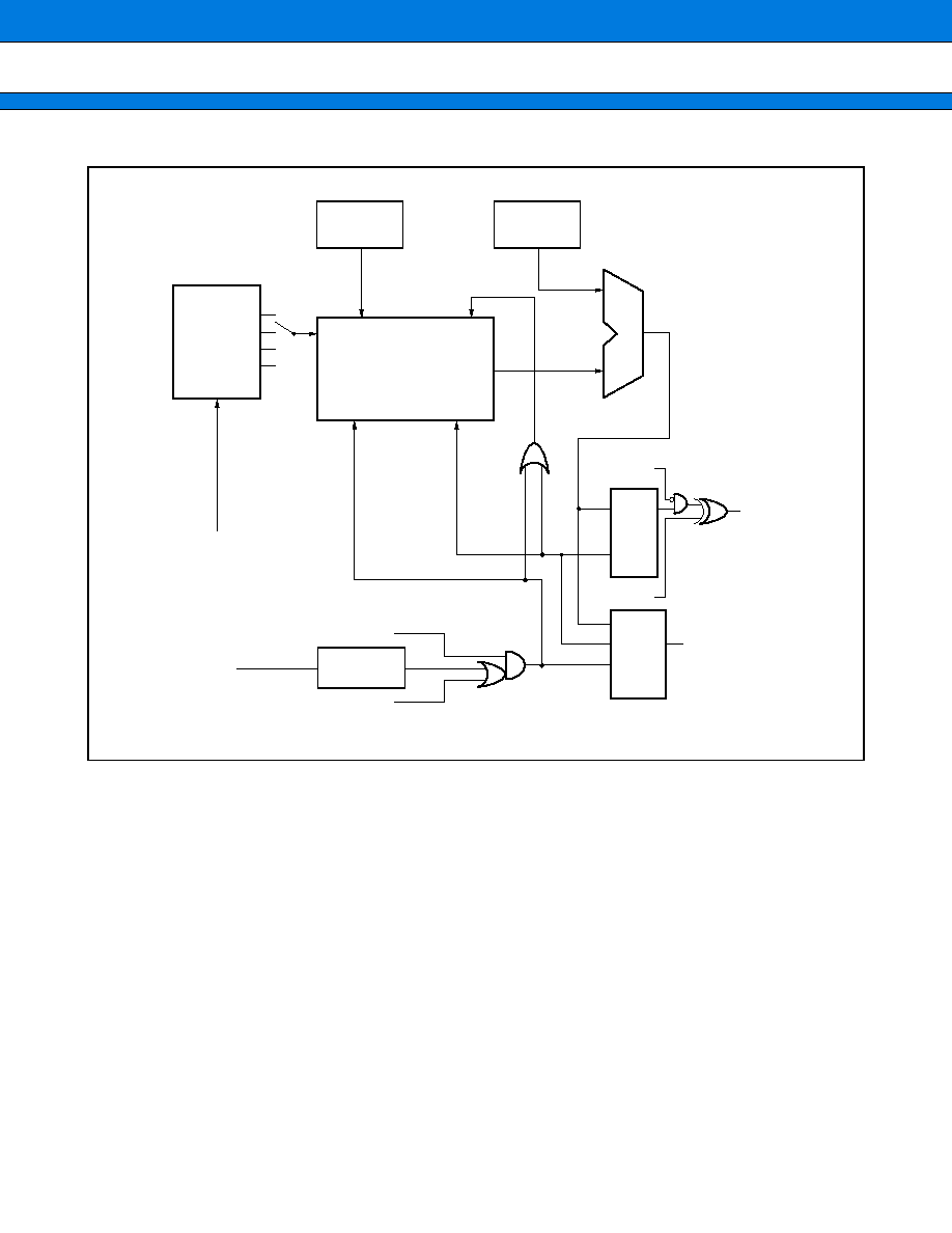
MB91F155A/MB91155/MB91154
49
· Block Diagram (for one channel)
1 / 1
1 / 4
1 / 16
1 / 64
ck
PCSR
Prescaler
Peripheral system clock
TRG input
Enable
PPG mask
PWM output
Inverse bit
Interrupt
selection
Soft trigger
Load
16-bit down counter
Start
Edge
detection
Borrow
PDUT
cmp
S
R
Q
IRQ

MB91F155A/MB91155/MB91154
50
· Register List
(Continued)
GCN1
GCN2
PTMR0
PCSR0
PDUT0
PCNH0
PCNL0
PTMR1
PCSR1
PDUT1
PCNH1
PCNL1
PTMR2
PCSR2
PDUT2
PCNH2
(R/W)
(R/W)
(R )
(W)
(W)
(R/W)
(R/W)
(R)
(W)
(W)
(R/W)
(R/W)
(R)
(W)
(W)
(R/W)
bit 8
bit 15
Address
bit 0
Initial value
0 0 1 1 0 0 1 0
B
0 0 0 1 0 0 0 0
B
0 0 0 0 0 0 0 0
B
1 1 1 1 1 1 1 1
B
1 1 1 1 1 1 1 1
B
XXXXXXXX
B
XXXXXXXX
B
XXXXXXXX
B
XXXXXXXX
B
0 0 0 0 0 0 0 -
B
0 0 0 0 0 0 0 0
B
1 1 1 1 1 1 1 1
B
1 1 1 1 1 1 1 1
B
XXXXXXXX
B
XXXXXXXX
B
XXXXXXXX
B
XXXXXXXX
B
0 0 0 0 0 0 0 -
B
0 0 0 0 0 0 0 0
B
1 1 1 1 1 1 1 1
B
1 1 1 1 1 1 1 1
B
XXXXXXXX
B
XXXXXXXX
B
XXXXXXXX
B
XXXXXXXX
B
0 0 0 0 0 0 0 -
B
00000094
H
00000095
H
00000097
H
00000098
H
00000099
H
0000009A
H
0000009B
H
0000009C
H
0000009D
H
0000009E
H
0000009F
H
000000A0
H
000000A1
H
000000A2
H
000000A3
H
000000A4
H
000000A5
H
000000A6
H
000000A7
H
000000A8
H
000000A9
H
000000AA
H
000000AB
H
000000AC
H
000000AD
H
000000AE
H
PCNL2
PTMR3
PCSR3
PDUT3
PCNH3
PCNL3
(R/W)
(R/W)
(R)
(W)
(W)
(R/W)
(R/W)
0 0 0 0 0 0 0 0
B
1 1 1 1 1 1 1 1
B
1 1 1 1 1 1 1 1
B
XXXXXXXX
B
XXXXXXXX
B
XXXXXXXX
B
XXXXXXXX
B
0 0 0 0 0 0 0 -
B
0 0 0 0 0 0 0 0
B
000000AF
H
000000B0
H
000000B1
H
000000B2
H
000000B3
H
000000B4
H
000000B5
H
000000B6
H
000000B7
H
(
) : Access R/W : Read/Write enabled R : Read only W : Write only
: Not in use
X : Undefined

MB91F155A/MB91155/MB91154
51
(Continued)
PTMR4
PCSR4
PDUT4
PCNH4
PCNL4
PTMR5
PCSR5
PDUT5
PCNH5
PCNL5
(R )
(W)
(W)
(R/W)
(R/W)
(R)
(W)
(W)
(R/W)
(R/W)
1 1 1 1 1 1 1 1
B
1 1 1 1 1 1 1 1
B
XXXXXXXX
B
XXXXXXXX
B
XXXXXXXX
B
XXXXXXXX
B
0 0 0 0 0 0 0 -
B
0 0 0 0 0 0 0 0
B
1 1 1 1 1 1 1 1
B
1 1 1 1 1 1 1 1
B
XXXXXXXX
B
XXXXXXXX
B
XXXXXXXX
B
XXXXXXXX
B
0 0 0 0 0 0 0 -
B
0 0 0 0 0 0 0 0
B
000000B8
H
000000B9
H
000000BA
H
000000BB
H
000000BC
H
000000BD
H
000000BE
H
000000BF
H
000000C0
H
000000C1
H
000000C2
H
000000C3
H
000000C4
H
000000C5
H
000000C6
H
000000C7
H
bit 8
bit 15
Address
bit 0
Initial value
(
) : Access
R/W : Read/Write enabled
R : Read only
W : Write only
: Not in use
X : Undefined

MB91F155A/MB91155/MB91154
52
5.
16-bit Reload Timer
The 16-bit reload timer consists of a 16-bit down counter, a 16-bit reload register, a prescaler for creating internal
count clocks, and a control register.
The input clock can be selected from three internal clock types (2/8/32 machine clock divisions) .
DMA transfer can be invoked by interrupt.
This product type contains this 16-bit reload timer for four channels.
· Block Diagram
RELD
OUTE
OUTL
INTE
UF
CNTE
TRG
OUT
CTL.
CSL1
CSL0
MOD2
MOD1
MOD0
16
16-bit reload register
16-bit down counter
8
16
2
3
2
Clock selector
IN CTL.
2
2
2
1
3
5
3
EXCK
Internal clocks
Clear
prescaler
GATE
Retrigger
UF
Reload
R bus
2
IRQ
PWM (ch0, ch1)
A/D (ch2)

MB91F155A/MB91155/MB91154
53
· Register List
TMCSR0
TMCSR1
TMCSR2
TMCSR3
TMR0
TMR1
TMR2
TMR3
TMRLR0
TMRLR1
(R/W)
(R/W)
(R/W)
(R/W)
(R)
(R)
(R)
(R)
(W)
(W)
- - - - 0 0 0 0
B
0 0 0 0 0 0 0 0
B
- - - - 0 0 0 0
B
0 0 0 0 0 0 0 0
B
- - - - 0 0 0 0
B
0 0 0 0 0 0 0 0
B
- - - - 0 0 0 0
B
0 0 0 0 0 0 0 0
B
XXXXXXXX
B
XXXXXXXX
B
XXXXXXXX
B
XXXXXXXX
B
XXXXXXXX
B
XXXXXXXX
B
XXXXXXXX
B
XXXXXXXX
B
XXXXXXXX
B
XXXXXXXX
B
XXXXXXXX
B
XXXXXXXX
B
00000032
H
00000033
H
0000003A
H
0000003B
H
00000042
H
00000043
H
0000004A
H
0000004B
H
0000002E
H
0000002F
H
00000036
H
00000037
H
0000003E
H
0000003F
H
00000046
H
00000047
H
0000002C
H
0000002D
H
00000034
H
00000035
H
TMRLR2
TMRLR3
(W)
(W)
XXXXXXXX
B
XXXXXXXX
B
XXXXXXXX
B
XXXXXXXX
B
0000003C
H
0000003D
H
00000044
H
00000045
H
bit 15
Address
bit 0
Initial value
(
) : Access
R/W : Read/Write enabled
R : Read only
W : Write only
: Not in use
X : Undefined

MB91F155A/MB91155/MB91154
54
6.
Bit Search Module
The module searches data written to the input register for "0" or "1" or a "change" and returns the detected bit
position.
· Block Diagram
· Register List
D bus
Address
decoder
Detection
mode
Input latch
Changing one detection into data
Bit search circuit
Search results
000003F0
H
000003F1
H
000003F2
H
000003F3
H
000003F4
H
000003F5
H
000003F6
H
000003F7
H
000003F8
H
000003F9
H
000003FA
H
000003FB
H
XXXXXXXX
B
XXXXXXXX
B
XXXXXXXX
B
XXXXXXXX
B
XXXXXXXX
B
XXXXXXXX
B
XXXXXXXX
B
XXXXXXXX
B
XXXXXXXX
B
XXXXXXXX
B
XXXXXXXX
B
XXXXXXXX
B
(W)
(R/W)
(W)
BSD0
bit 16
bit 31
Address
bit 0
Initial value
BSD1
BSDC
000003FC
H
000003FD
H
000003FE
H
000003FF
H
XXXXXXXX
B
XXXXXXXX
B
XXXXXXXX
B
XXXXXXXX
B
(R)
BSRR
(
) : Access
R/W : Read/Write enabled
R : Read only
W : Write only
X : Undefined

MB91F155A/MB91155/MB91154
55
7.
8/10-bit A/D Converter (Sequential Conversion Type)
The A/D converter is a module that converts analog input voltage into a digital value. Its features are as follows :
· A minimum conversion time of 5.0
µ
s/ch. (Including sampling time at a 33 MHz machine clock)
· Contains a sample and hold circuit.
· Resolution : 10 or 8 bits selectable.
· Selection of analog input from eight channels by program
· DMA transfer can be invoked by interrupt.
· Selection of an invoking factor from software, external pin trigger (falling edge) , and 16-bit reload timer (rising
edge) .
· Block Diagram
Single conversion mode :
Selects and converts one channel.
Continuous conversion mode : Converts a specified channel repeatedly.
Stop and convert mode :
Stops after converting one channel and stands by until invoked the next time.
(Conversion invoking can be synchronized.)
MP
Decoder
Comparator
Data register
A/D control register 1
A/D control register 2
Sample & hold circuit
AN0
AN1
AN2
AN3
AN4
AN5
AN6
AN7
ADCR
D/A converter
Sequential compare
register
Input
circuit
ADCS1
,
2
Operating clock
Prescaler
16-bit reload timer 2
External pin trigger
AV
SS
AVR
±
AV
SS
R - BUS

MB91F155A/MB91155/MB91154
56
· Register List
ADCR
ADCS1
ADCS0
AICK
(W, R)
(R)
(R/W, W)
(R/W)
(R/W)
0 0 1 0 1 - X X
B
XXXXXXXX
B
0 0 0 0 0 0 0 0
B
0 0 0 0 0 0 0 0
B
0 0 0 0 0 0 0 0
B
000000E4
H
000000E5
H
000000E6
H
000000E7
H
000000EB
H
bit 15
bit 0
(
) : Access
R/W : Read/Write enabled
R : Read only
W : Write only
: Not in use
X : Undefined

MB91F155A/MB91155/MB91154
57
8.
Interrupt Controller
The interrupt controller accepts and arbitrates interrupts.
· Block Diagram
to LEVEL0*
4
IM
NMI processing
Level
determination
Vector
determination
Level vector
generation
Priority determination
INT0*
2
OR
NMI*
6
.
.
.
RI00
RI47
(DLYIRQ)
.
.
.
DLYI*
1
.
.
ICR00
ICR47
4
5
5
Request to
withdraw
HLDREQ
6
R bus
6
LEVEL4
HLDCAN*
3
to VCT0*
5
VCT5
*1 : DLY1 represents the delay interrupt module (delay interrupt generator) . (For detailed information, see
section 10, "Delay Interrupt Module."
*2 : INT0 is a wake-up signal for the clock controller in sleep or stop mode.
*3 : HLDCAN is a bus surrender request signal for bus masters except for the CPU.
*4 : LEVEL 4 - 0 are interrupt level outputs.
*5 : VCT 5 - 0 are interrupt vector outputs.
*6 : This product type does not have the NMI function.

MB91F155A/MB91155/MB91154
58
· Register List
(Continued)
ICR00
00000400
H
(R/W)
- - - - 1 1 1 1
B
ICR01
00000401
H
(R/W)
- - - - 1 1 1 1
B
ICR02
00000402
H
(R/W)
- - - - 1 1 1 1
B
ICR03
00000403
H
(R/W)
- - - - 1 1 1 1
B
ICR04
00000404
H
(R/W)
- - - - 1 1 1 1
B
ICR05
00000405
H
(R/W)
- - - - 1 1 1 1
B
ICR06
00000406
H
(R/W)
- - - - 1 1 1 1
B
ICR07
00000407
H
(R/W)
- - - - 1 1 1 1
B
ICR08
00000408
H
(R/W)
- - - - 1 1 1 1
B
ICR09
00000409
H
(R/W)
- - - - 1 1 1 1
B
ICR10
0000040A
H
(R/W)
- - - - 1 1 1 1
B
ICR11
0000040B
H
(R/W)
- - - - 1 1 1 1
B
ICR12
0000040C
H
(R/W)
- - - - 1 1 1 1
B
ICR13
0000040D
H
(R/W)
- - - - 1 1 1 1
B
ICR14
0000040E
H
(R/W)
- - - - 1 1 1 1
B
ICR15
0000040F
H
(R/W)
- - - - 1 1 1 1
B
ICR16
00000410
H
(R/W)
- - - - 1 1 1 1
B
ICR17
00000411
H
(R/W)
- - - - 1 1 1 1
B
ICR18
00000412
H
(R/W)
- - - - 1 1 1 1
B
ICR19
00000413
H
(R/W)
- - - - 1 1 1 1
B
ICR20
00000414
H
(R/W)
- - - - 1 1 1 1
B
ICR21
00000415
H
(R/W)
- - - - 1 1 1 1
B
ICR22
00000416
H
(R/W)
- - - - 1 1 1 1
B
ICR23
00000417
H
(R/W)
- - - - 1 1 1 1
B
ICR24
00000418
H
(R/W)
- - - - 1 1 1 1
B
ICR25
00000419
H
(R/W)
- - - - 1 1 1 1
B
ICR26
0000041A
H
(R/W)
- - - - 1 1 1 1
B
ICR27
0000041B
H
(R/W)
- - - - 1 1 1 1
B
ICR28
0000041C
H
(R/W)
- - - - 1 1 1 1
B
ICR29
0000041D
H
(R/W)
- - - - 1 1 1 1
B
ICR30
0000041E
H
(R/W)
- - - - 1 1 1 1
B
ICR31
0000041F
H
(R/W)
- - - - 1 1 1 1
B
ICR32
00000420
H
(R/W)
- - - - 1 1 1 1
B
ICR33
00000421
H
(R/W)
- - - - 1 1 1 1
B
ICR34
00000422
H
(R/W)
- - - - 1 1 1 1
B
ICR35
00000423
H
(R/W)
- - - - 1 1 1 1
B
ICR36
00000424
H
(R/W)
- - - - 1 1 1 1
B
ICR37
00000425
H
(R/W)
- - - - 1 1 1 1
B
ICR38
00000426
H
(R/W)
- - - - 1 1 1 1
B
ICR39
00000427
H
(R/W)
- - - - 1 1 1 1
B
bit 7
bit 0
bit 7
bit 0
Address
Initial value
Address
Initial value
(
) : Access
R/W : Read/Write enabled
: Not in use

MB91F155A/MB91155/MB91154
59
(Continued)
ICR40
00000428
H
(R/W)
- - - - 1 1 1 1
B
ICR41
00000429
H
(R/W)
- - - - 1 1 1 1
B
ICR42
0000042A
H
(R/W)
- - - - 1 1 1 1
B
ICR43
0000042B
H
(R/W)
- - - - 1 1 1 1
B
ICR44
0000042C
H
(R/W)
- - - - 1 1 1 1
B
ICR45
0000042D
H
(R/W)
- - - - 1 1 1 1
B
ICR46
0000042E
H
(R/W)
- - - - 1 1 1 1
B
ICR47
0000042F
H
(R/W)
- - - - 1 1 1 1
B
HRCL
00000431
H
(R/W)
- - - - 1 1 1 1
B
DICR
00000430
H
(R/W)
- - - - - - - 0
B
bit 7
bit 0
Address
Initial value
(
) : Access
R/W : Read/Write enabled
: Not in use

MB91F155A/MB91155/MB91154
60
9.
External Interrupt
The external interrupt controller controls external interrupt requests input to INT pins 0 through 15.
The level of requests to be detected can be selected from "H, " "L, " rising edge, and falling edge.
· Block Diagram
· Register List
10. Delay Interrupt Module
The delay interrupt is a module that generates task switching interrupts. The use of this module allows the
software to generate/cancel interrupt requests to the CPU.
For the block diagram of the delay interrupt module, see section 8, "Interrupt Controller."
· Register List
16
Interrupt permission register
Interrupt factor register
Request level setting register
R bus
16
32
16
Interrupt
request
Gate
Factor F/F
Edge detection
circuit
16
INT0 to INT15
EIRR0
EIRR1
ENIR0
ENIR1
ELVR0
ELVR1
(R/W)
(R/W)
(R/W)
(R/W)
0 0 0 0 0 0 0 0
B
0 0 0 0 0 0 0 0
B
0 0 0 0 0 0 0 0
B
0 0 0 0 0 0 0 0
B
0 0 0 0 0 0 0 0
B
0 0 0 0 0 0 0 0
B
0 0 0 0 0 0 0 0
B
0 0 0 0 0 0 0 0
B
000000C8
H
000000C9
H
000000CA
H
000000CB
H
000000CC
H
000000CD
H
000000CE
H
000000CF
H
bit 8
bit 15
Address
bit 0
Initial value
(
) : Access
R/W : Read/Write enabled
DICR
(R/W)
bit 7
Address
bit 0
Initial value
- - - - - - - 0
B
00000430
H
(
) : Access
R/W : Read/Write enabled
: Not in use

MB91F155A/MB91155/MB91154
61
11. Clock Generator (Low power consumption mechanism)
The clock generator is responsible for the following functions :
· CPU clock generation (including the gear function)
· Peripheral clock generation (including the gear function)
· Reset generation and holding factors
· Standby function (including hardware standby)
· Contains PLL (multiplication circuit)
· Block Diagram
X0
[Gear controller]
[Stop/sleep controller]
[Reset factor circuit]
[Watchdog controller]
GCR register
CPU gear
CPU Clock
Internal bus clock
Stop state
Sleep state
CPU Hold request
Internal reset
Internal
peripheral clock
Peripheral
gear
Internal clock
generating
circuit
Status
transition
control
circuit
Oscillator
circuit
X1
V
CC
Power on
detection circuit
GND
RSRR register
WPR register
Timebase timer
CTBR register
Watchdog F/F
Count clock
RST pin
M
P
X
PLL
Reset
generating
F/F
STCR register
PDRR register
Internal interrupt
Internal reset
DMA request
1
/
2
R

MB91F155A/MB91155/MB91154
62
· Register List
RSRR
/
WTCH
STCR
PDRR
CTBR
GCR
WPR
(R/W, W)
(W)
(R/W, R)
(W)
bit 8
bit 15
bit 0
000111--
B
(R, W)
1-XXX-00
B
(R/W)
----0000
B
XXXXXXXX
B
110011-1
B
XXXXXXXX
B
00000481
H
00000482
H
00000483
H
00000480
H
00000484
H
00000485
H
Address
Initial value
(
) : Access
R/W : Read/Write enabled
R : Read only
W : Write only
: Not in use
X : Undefined

MB91F155A/MB91155/MB91154
63
12. External Bus Interface
The external bus interface controls the interface between the external memory and the external I/O. Its features
are as follows :
· 24-bit (16 MB) address output
· An 8/16-bit bus width can be set by chip select area.
· Inserts an automatic and programmable memory wait (for seven cycles at maximum) .
· Unused addresses/data pins are available as I/O ports.
· Support for little endian mode
· Use of a clock doubler, 33 MHz internal and 16.5 MHz external bus operations
· Block Diagram
Write
buffer
Read
buffer
Address
buffer
Switch
Switch
A-Out
M
U
X
External DATA Bus
ASR
AMR
Registers
&
Control
External pin controller
3
4
4
Shifter
Comparator
Controls all blocks.
Inpage
+
1 or
+
2
DATA BLOCK
ADDRESS BLOCK
External
Address Bus
CS0 to CS3
RD
WR0, WR1
BRQ
BGRNT
RDY
CLK
ADDRESS B
U
S
D
ATA
B
U
S
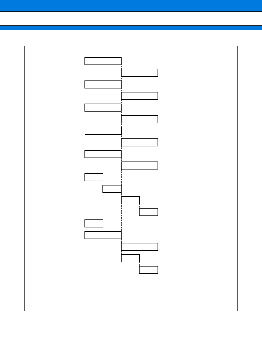
MB91F155A/MB91155/MB91154
64
· Register List
ASR1
AMR1
ASR2
AMR2
ASR3
AMR3
ASR4
AMR4
ASR5
AMR5
AMD0
AMD1
AMD32
AMD4
AMD5
EPCR0
(W)
(W)
(R/W)
(R/W)
(R/W)
(R/W)
(R/W)
bit 16
bit 31
bit 0
0 0 0 0 0 0 0 0
B
0 0 0 0 0 0 0 1
B
0 0 0 0 0 0 0 0
B
0 0 0 0 0 0 1 0
B
(W)
0 0 0 0 0 0 0 0
B
0 0 0 0 0 0 0 0
B
(W)
0 0 0 0 0 0 0 0
B
0 0 0 0 0 0 1 1
B
(W)
0 0 0 0 0 0 0 0
B
0 0 0 0 0 0 0 0
B
(W)
(W)
0 0 0 0 0 0 0 0
B
0 0 0 0 0 1 0 0
B
(W)
0 0 0 0 0 0 0 0
B
0 0 0 0 0 0 0 0
B
0 0 0 0 0 0 0 0
B
0 0 0 0 0 0 0 0
B
(W)
0 0 0 0 0 0 0 0
B
0 0 0 0 0 0 0 0
B
(W)
0 0 0 0 0 0 0 0
B
0 0 0 0 0 1 0 1
B
(W)
- - - - - - - -
B
1 1 1 1 1 1 1 1
B
(W)
- - - - 1 1 0 0
B
- 1 1 1 1 1 1 1
B
- - - 0 0 1 1 1
B
0 - - 0 0 0 0 0
B
0 0 0 0 0 0 0 0
B
0 - - 0 0 0 0 0
B
0 - - 0 0 0 0 0
B
0000060C
H
0000060D
H
0000060E
H
0000060F
H
00000610
H
00000611
H
00000612
H
00000613
H
00000614
H
00000615
H
00000616
H
00000617
H
00000618
H
00000619
H
0000061A
H
0000061B
H
0000061C
H
0000061D
H
0000061E
H
0000061F
H
00000628
H
00000629
H
0000062A
H
0000062B
H
00000620
H
00000621
H
00000622
H
00000623
H
00000624
H
000007FE
H
EPCR1
LER
MODR
(W)
(W)
- - - - - 0 0 0
B
XXXXXXXX
B
000007FF
H
Address
Initial value
(
) : Access
R/W : Read/Write enabled
W : Write only
: Not in use
X : Undefined

MB91F155A/MB91155/MB91154
65
13. Multifunction Timer
The multifunction timer unit consists of one 16-bit free-run timer, eight 16-bit output compare registers, four 16-
bit input capture registers, and six 16-bit PPG timer channels. By using this function waveforms can be output
based on the 16-bit free-run timer and the input pulse width and external clock cycle can also be measured.
· Timer Components
· 16-bit free-run timer (
×
1)
The 16-bit free-run timer consists of a 16-bit up counter, a control register, a 16-bit compare clear register,
and a prescaler. The output value of this counter is used as the basic time (base timer) for output compare
and input capture.
· Output compare (
×
8)
The output compare consists of eight 16-bit compare registers, a compare output latch, and a control register.
When the 16-bit free-run timer value agrees to the compare register value, the output level can be inverted
and an interrupt can also be generated.
· Input capture (
×
4)
The input capture consists of capture registers corresponding to four independent external input pins and a
control register. By detecting any edge of signals input from external input pins, the 16-bit free-run timer value
can be held in the capture register and an interrupt can be generated at the same time.
· 16-bit PPG timer (
×
6)
See the section on the PPG Timer.

MB91F155A/MB91155/MB91154
66
· Block Diagram
IVF
R-BUS
IVFE
STOP
Interrupt
Interrupt
Interrupt
Interrupt
Interrupt
Interrupt
16-bit free-run timer
Compare register 0/2/4/6
Compare circuit
Compare register 1/3/5/7
Compare circuit
Capture register 0/2
Capture register 1/3
16-bit compare clear register
(Channel 6's compare register)
MODE
SCLR
CLK2
CLK1
CLK0
Divider
Compare circuit
Clock
ICLR
IOP1
IOP0
IOE1
IOE0
ICP0
ICP1
ICE0
ICE1
EG11
EG10
EG01
EG00
IN 0/2
IN 1/3
CMOD
Select
OC0/2/4/6
T
Q
OC1/3/5/7
T
Edge detection
Edge detection
Q
ICRE
MS13 to 0

MB91F155A/MB91155/MB91154
67
· Register List
bit15
bit8 bit7
bit0
IPCP1
IPCP0
IPCP3
IPCP2
OCCP1
OCCP0
OCCP3
OCCP2
OCCP5
OCCP4
OCCP7
OCCP6
OCS3,2
OCS1,0
OCS7,6
OCS5,4
TCDT
TCCS
ICS23
ICS01
000068
H
000069
H
00006A
H
00006B
H
00006C
H
00006D
H
00006E
H
00006F
H
000071
H
000073
H
000074
H
000075
H
000076
H
000077
H
000078
H
000079
H
00007A
H
00007B
H
00007C
H
00007D
H
00007E
H
00007F
H
000080
H
000081
H
000082
H
000083
H
000084
H
000085
H
000086
H
000087
H
000088
H
000089
H
00008A
H
00008B
H
00008C
H
00008D
H
00008E
H
00008F
H
XXXXXXXX
B
( R )
XXXXXXXX
B
( R )
XXXXXXXX
B
( R )
XXXXXXXX
B
( R )
XXXXXXXX
B
( R )
XXXXXXXX
B
( R )
XXXXXXXX
B
( R )
XXXXXXXX
B
( R )
00000000
B
( R/W )
00000000
B
( R/W )
XXXXXXXX
B
( R/W )
XXXXXXXX
B
( R/W )
XXXXXXXX
B
( R/W )
XXXXXXXX
B
( R/W )
XXXXXXXX
B
( R/W )
XXXXXXXX
B
( R/W )
XXXXXXXX
B
( R/W )
XXXXXXXX
B
( R/W )
XXXXXXXX
B
( R/W )
XXXXXXXX
B
( R/W )
XXXXXXXX
B
( R/W )
XXXXXXXX
B
( R/W )
XXXXXXXX
B
( R/W )
XXXXXXXX
B
( R/W )
XXXXXXXX
B
( R/W )
XXXXXXXX
B
( R/W )
XXX00000
B
( R/W )
0000XX00
B
( R/W )
XXX00000
B
( R/W )
0000XX00
B
( R/W )
XXX00000
B
( R/W )
0000XX00
B
( R/W )
XXX00000
B
( R/W )
0000XX00
B
( R/W )
00000000
B
( R/W )
00000000
B
( R/W )
0 - - - - - - -
B
( R/W )
00000000
B
( R/W )
Address
Initial value
(
) : Access R/W : Read/Write enabled R : Read only
: Not in use
X : Undefined

MB91F155A/MB91155/MB91154
68
14. Calendar Macro
This macro is a calendar macro with a basic clock of 32.768 kHz.
The macro accomplishes clock functions including, year, month, date, hour, minutes, seconds, day of the week,
and leap years.
The macro counts the last two digits of calendar years 0 through 99.
· Block Diagram
· Register List
32 kHz
Oscillator
Calendar circuit
Bus
controller
D
b
u
s
bit15
Address
bit8
bit17
bit0
Initial value
CAC
CA1
CA2
CA3
CA4
CA5
CA6
CA7
CAS
000210
H
000211
H
00000000
B
( R/W )
- - XXXXXX
B
( R/W )
000212
H
000213
H
- - XXXXXX
B
( R/W )
- - - XXXXX
B
( R/W )
000214
H
000215
H
- - -XXXXX
B
( R/W )
- - - - - XXX
B
( R/W )
000216
H
000217
H
- - - - XXXX
B
( R/W )
- XXXXXXX
B
( R/W )
00021F
H
0 - - - - - - 0
B
( R/W )
(
) : Access
R/W : Read/Write enabled
: Not in use
X : Undefined

MB91F155A/MB91155/MB91154
69
15. I
2
C Interface
The I
2
C interface is a serial I/O port that supports the Inter IC BUS and operates as a master/slave device on
the I
2
C bus.
· Features of the I
2
C Interface
Contains one I
2
C interface channel.
The interface has the following features :
· Master/slave send and receive
· Arbitration function
· Clock synchronization function
· Slave address/general call address detection function
· Transfer direction detection function
· Repeated generation and detection of start conditions
· Bus error detection function
· Register List
· Bus control register (IBCR)
· Bus status register (IBSR)
· Address register (IADR)
· Clock control register (ICCR)
· Data register (IDAR)
R/W : Read/Write enabled, R : Read only,
: Not in use, X : Undefined
Address
Initial value
0000-0120
H
00000000
B
Address
Initial value
0000-0121
H
00000000
B
Address
Initial value
0000-0122
H
- XXXXXXX
B
Address
Initial value
0000-0123
H
-
-
0XXXXX
B
Address
Initial value
0000-0125
H
XXXXXXXX
B
R/W
R/W
R/W
R/W
R/W
R/W
R/W
R/W
bit 15
bit 14
bit 13
bit 12
bit 11
bit 10
bit 9
bit 8
BER
BEIE
SCC
MSS
ACK
GCAA
INTE
INT
R
R
R
R
R
R
R
R
bit 7
bit 6
bit 5
bit 4
bit 3
bit 2
bit 1
bit 0
BB
RSC
AL
LRB
TR
AAS
GCA
FBT
R/W
R/W
R/W
R/W
R/W
R/W
R/W
bit 15
bit 14
bit 13
bit 12
bit 11
bit 10
bit 9
bit 8
A6
A5
A4
A3
A2
A1
A0
R/W
R/W
R/W
R/W
R/W
R/W
bit 7
bit 6
bit 5
bit 4
bit 3
bit 2
bit 1
bit 0
EN
CS4
CS3
CS2
CS1
CS0
R/W
R/W
R/W
R/W
R/W
R/W
R/W
R/W
bit 7
bit 6
bit 5
bit 4
bit 3
bit 2
bit 1
bit 0
D7
D6
D5
D4
D3
D2
D1
D0

MB91F155A/MB91155/MB91154
70
· Block Diagram
EN
I
2
C enable
Peripheral clock
Clock division 1
Clock selection 1
Clock division 2
Shift clock generation
Clock selection 2
R bus
ICCR
IBCR
IBCR
Start
Master
Slave
Global call
ACK permission
GC-ACK permission
IBSR
Slave address
comparison
IBSR
BB
BER
SCC
MSS
ACK
AAS
GCAA
GCA
IADR
IRQ
End
Start/stop condition detection
SDA
SCL
First Byte
Error
Start/stop condition detection
Arbitration lost detection
Interrupt request
Last Bit
Bus busy
Send/Receive
Repeat start
Sync
Shift clock
edge variation timing
IDAR
BEIE
INTE
INT
RSC
LRB
TR
FBT
AL
CS4
CS3
CS2
CS1
CS0
2
4
8
16
5
6
7
8
32
64
128
256
ICCR

MB91F155A/MB91155/MB91154
71
16. FLASH Memory
The MB91F155A contains a 510-Kbyte (4 Mbits) flash memory. The sectors can be erased all at once or sector
by sector and that can be written with the FR-CPU by half word (16 bits) using a single 0.3 V power supply.
The MB91F155 accomplishes the following functions by a combination of the flash memory macro and the FR-
CPU interface circuit :
· Functions as the CPU program/data storage memory :
When used as a ROM, the memory is accessible with a 32-bit bus width.
Allows the CPU to read from/write to/erase the memory (automatic program algorithm*) .
· Functions equivalent to the stand-alone MBM29LV400C flash memory product :
Allows a ROM programmer to read from/write to/erase the memory (automatic program algorithm*)
At this time, using the flash memory from the FR-CPU is described. For detailed information about using the
flash memory from the ROM programmer, refer to the ROM programmer instruction manual.
* : Automatic program algorithm
=
Embedded Algorithm
TM
Embedded Algorithm
TM
is a trademark of Advanced Micro Devices, Inc.
· Block Diagram
RDY/BUSY
Rising edge detection
Flash memory
Control signal
generation
RESET
BYTE
OE
WE
CE
FA18 - 0
Address buffer
FR-C bus (instructions/data)
Data buffer
CA18 - 0
INTE
Interrupt requests
Bus control signals
RDYINT
RDY
WE
CD31 - 0
DI15 - 0
DO31 - 0

MB91F155A/MB91155/MB91154
72
· Memory Map
Flash memory address mapping varies between FLASH memory mode and CPU mode. Mapping in each mode
is shown next.
SA6
SA5
SA4
SA3
SA2
SA1
SA0
SA13
SA12
SA11
SA10
SA9
SA8
SA7
( SAn : sector address n )
0FFFFF
H
0FFFFF
H
0F8000
H
0F4000
H
0F0000
H
0E0000
H
0C0000
H
080000
H
080800
H
080000
H
0007C0
H
000000
H
0A0000
H
080800
H
CPU mode
FLASH memory area
RAM area 2 Kbytes
Status register
SA13
SA12
SA11
SA10
SA9
SA8
SA7
SA6
SA5
SA4
SA3
SA2
SA1
SA0
( SAn : sector address n )
0FFFFF
H
FLASH
memory image
07FFFF
H
010000
H
000000
H
FLASH memory mode
Memory mapping in FLASH memory mode of MB91F155A :
Memory mapping in CPU mode of MB91F155A :

MB91F155A/MB91155/MB91154
73
· Sector Address Table
· Registers
FLCR : Status register (CPU mode)
This register indicates the FLASH memory operating status. The register controls interrupts to the CPU as well
as writing to the FLASH memory.
This register is accessible only in CPU mode. Do not access this register with read modify write instructions.
FWTC : Wait register
This register controls waiting for the FLASH memory in CPU mode.
The register also controls accessing to read from the FLASH memory (33 MHz operations) at high speeds.
Sector address
Address range
Corresponding bit
positions
Sector capacity
SA7
080802, 3
H
to 09FFFE, F
H
(16 bits on LSB side)
bit15 to 0
64 Kbyte
SA8
0A0002, 3
H
to 0BFFFE, F
H
(16 bits on LSB side)
bit15 to 0
64 Kbyte
SA9
0C0002, 3
H
to 0DFFFE, F
H
(16 bits on LSB side)
bit15 to 0
64 Kbyte
SA10
0E0002, 3
H
to 0EFFFE, F
H
(16 bits on LSB side)
bit15 to 0
32 Kbyte
SA11
0F0002, 3
H
to 0F3FFE, F
H
(16 bits on LSB side)
bit15 to 0
8 Kbyte
SA12
0F4002, 3
H
to 0F7FFE, F
H
(16 bits on LSB side)
bit15 to 0
8 Kbyte
SA13
0F8002, 3
H
to 0FFFFE, F
H
(16 bits on LSB side)
bit15 to 0
16 Kbyte
SA0
080800, 1
H
to 09FFFC, D
H
(16 bits on MSB side)
bit31 to 16
64 Kbyte
SA1
0A0000, 1
H
to 0BFFFC, D
H
(16 bits on MSB side)
bit31 to 16
64 Kbyte
SA2
0C0000, 1
H
to 0DFFFC, D
H
(16 bits on MSB side)
bit31 to 16
64 Kbyte
SA3
0E0000, 1
H
to 0EFFFC, D
H
(16 bits on MSB side)
bit31 to 16
32 Kbyte
SA4
0F0000, 1
H
to 0F3FFC, D
H
(16 bits on MSB side)
bit31 to 16
8 Kbyte
SA5
0F4000, 1
H
to 0F7FFC, D
H
(16 bits on MSB side)
bit31 to 16
8 Kbyte
SA6
0F8000, 1
H
to 0FFFFC, D
H
(16 bits on MSB side)
bit31 to 16
16 Kbyte
R/W
( 0 )
R/W
( 0 )
R
( X )
( X )
( X )
( X )
R/W
( 0 )
bit 7
bit 6
bit 5
bit 4
bit 3
bit 2
bit 1
bit 0
RDYINT
R/W
( 0 )
INTE
WE
RDY
LPM
0007C0
H
R/W : Read/Write enabled, R : Read only,
: Not in use, X : Undefined
(
)
(
)
(
)
(
)
W
( 0 )
R/W
( 0 )
R/W
( 0 )
bit 7
bit 6
bit 5
bit 4
bit 3
bit 2
bit 1
bit 0
(
)
FACH
WTC1
WTC0
0007C4
H
R/W : Read/Write enabled, W : Write only,
: Not in use, X : Undefined

MB91F155A/MB91155/MB91154
74
17. 8-bit D/A Converter
This block is of an 8-bit resolution, R-2R D/A converter. The block contains three D/A converter channels and
each D/A control register can control output independently.
The D/A converter pin is a dedicated pin.
· Block Diagram
DA27
DA27
DA20
DA17
DA10
DA07
DA00
DAVC
DA20
DAE2
DAE1
DAE0
DA17
DAVC
DA10
DA07
DAVC
DA00
R
-
BUS
Standby control
Standby control
Standby control
D/A output channel 2
D/A output channel 1
D/A output channel 0

MB91F155A/MB91155/MB91154
75
· Register List
7
6
5
4
3
2
1
0
Initial value
DA06
DA07
DA05
DA04
DA03
DA02
DA01
DA00
DADR0
00000E3
H
bit
15
14
13
12
11
10
9
8
DA16
DA17
DA15
DA14
DA13
DA12
DA11
DA10
DADR1
00000E2
H
bit
23
22
21
20
19
18
17
16
DA26
DA27
DA25
DA24
DA23
DA22
DA21
DA20
DADR2
00000E1
H
bit
7
6
5
4
3
2
1
0
DAE0
DACR0
00000DF
H
bit
15
14
13
12
11
10
9
8
DAE1
DACR1
00000DE
H
bit
23
22
21
20
19
18
17
16
DAE2
DACR2
00000DD
H
bit
XXXXXXXX
B
( R/W )
XXXXXXXX
B
( R/W )
XXXXXXXX
B
( R/W )
- - - - - - - 0
B
( R/W )
- - - - - - - 0
B
( R/W )
- - - - - - - 0
B
( R/W )
( ) : Access, R/W : Read/Write enabled,
: Not in use, X : Undefined

MB91F155A/MB91155/MB91154
76
18. 8/16-bit Up/Down Counters/Timers
This is the up/down counter/timer block consisting of six event input pins, two 8-bit up/down counters, two 8-bit
reload/compare registers, and their control circuits.
The features of this module are as follows :
· Capable of counting in the (0) d- (256) d range by the 8-bit count register.
(In 16-bit
×
1 operating mode, the register can count in the (0) d- (65535) d range.)
· Four count modes to choose from by the count clock.
· In timer mode the count clock can be selected from two internal clock types.
· In up/down count mode an external pin input signal detection edge can be selected.
· The phase-difference count mode is suitable for encoder counting, such as of motors. Rotation angles, rotating
speeds, and so on can be counted accurately and easily by inputting the output of phases A, B, and Z.
· Two types of function to choose from for the ZIN pin. (Enabled in all modes)
· Equipped with compare and reload functions which can be used individually or in combination. When combined,
these functions can count up/down at any width.
· The immediately preceding count direction can be identified by the count direction flag.
· Capable of individually controlling interrupt generation when comparison results match, at occurrence of reload
(underflow) or overflow, or when the count direction changes.

MB91F155A/MB91155/MB91154
77
· Block Diagram
ZIN0
CGE1
UDCC
UCRE
Counter clear
RLDE
Carry
CMPF
OVFF
UDFF
UDIE
CITE
Counter clock
Interrupt output
UDF1
CSTR
BIN0
Prescaler
AIN0
CLKS
CES1
Up/down count
clock selection
CES0
CMS1
CMS0
UDF0
CDCF
CFIE
RCUT
Reload control
Edge/level detection
8 bit
RCR0
(Reload/compare register 0)
UDCR0
(Up/down count register 0)
Data bus
8 bit
CGE0
C/GS
· 8/16-bit Up/Down Counter/Timer (channel 0)

MB91F155A/MB91155/MB91154
78
ZIN1
CGE1
UDCC
UCRE
RLDE
Carry
Counter clock
Interrupt output
CMPF
OVFF
UDFF
UDIE
CITE
UDF1
CSTR
BIN1
AIN1
CLKS
Prescaler
CES1
CES0
M16E
CMS1
Up/down count
clock selection
CMS0
UDF0
CDCF
CFIE
RCUT
Counter clear
Reload control
Edge/level detection
8 bit
Data bus
RCR1
(Reload/compare register 1)
UDCR1
(Up/down count register 1)
8 bit
CGE0
C/GS
· 8/16-bit Up/Down Counter/Timer (channel 1)

MB91F155A/MB91155/MB91154
79
· Register List
( ) : Access, R/W : Read/Write enabled, R : Read only, W : Write only,
: Not in use, X : Undefined
Initial value
Address : 00005F
H
00000000
B
(R)
Initial value
Address : 00005E
H
00000000
B
(R)
Initial value
Address : 00005D
H
00000000
B
(W)
Initial value
Address : 00005C
H
00000000
B
(W)
Initial value
Address : 000063
H
00000000
B
(R/W)
Initial value
Address : 000067
H
00000000
B
(R/W)
Initial value
Address : 000061
H
-000X000
B
(R/W, W)
Initial value
Address : 000065
H
-000X000
B
(R/W, W)
Initial value
Address : 000060
H
00000000
B
(R/W)
Initial value
Address : 000064
H
-0000000
B
(R/W)
bit
7
6
5
4
3
2
1
0
UDCR0
bit
15
14
13
12
11
10
9
8
UDCR1
bit
7
6
5
4
3
2
1
0
RCR0
bit
15
14
13
12
11
10
9
8
RCR1
bit
7
6
5
4
3
2
1
0
CSR0
bit
7
6
5
4
3
2
1
0
CSR1
bit
7
6
5
4
3
2
1
0
CCRL0
bit
7
6
5
4
3
2
1
0
CCRL1
bit
15
14
13
12
11
10
9
8
CCRH0
bit
15
14
13
12
11
10
9
8
CCRH1

MB91F155A/MB91155/MB91154
80
19. Peripheral STOP Control
This function can be used to stop the clock of unused resources in order to conserve more power.
· Register List
bit7
bit0
STPR0
000090
H
0000 - - - -
B
( R/W )
STPR1
000091
H
00000000
B
( R/W )
STPR2
000092
H
000000 - -
B
( R/W )
Address
Initial value
( ) : Access, R/W : Read/Write enabled,
: Not in use

MB91F155A/MB91155/MB91154
81
s
s
s
s
ELECTRICAL CHARACTERISTICS
1.
Absolute Maximum Ratings
(V
SS
=
AV
SS
=
0.0 V)
*1 : Take care not to exceed V
CC
+
0.3 V when turning on the power, for example.
Take care also to prevent AV
CC
from exceeding V
CC
when turning on the power, for example.
*2 : The maximum output current stipulates the peak value of a single concerned pin.
*3 : The average output current stipulates the average current flowing through a single concerned pin over a period
of 100 ms.
*4 : The total average output current stipulates the average current flowing through all concerned pins over a period
of 100 ms.
WARNING: Semiconductor devices can be permanently damaged by application of stress (voltage, current,
temperature, etc.) in excess of absolute maximum ratings. Do not exceed these ratings.
Parameter
Symbol
Value
Unit
Remarks
Min
Max
Power supply voltage
V
CC
V
SS
-
0.3
V
SS
+
3.6
V
Analog supply voltage
AV
CC
V
SS
-
0.3
V
SS
+
3.6
V
*1
Analog reference voltage
AVRH
V
SS
-
0.3
V
SS
+
3.6
V
*1
Input voltage
V
I
V
SS
-
0.3
V
CC
+
0.3
V
Input voltage
(open drain port J)
V
I2
V
SS
-
0.3
V
SS
+
5.5
V
Analog pin input voltage
V
IA
V
SS
-
0.3
AV
CC
+
0.3
V
Output voltage
V
O
V
SS
-
0.3
V
CC
+
0.3
V
"L" level maximum output current
I
OL
10
mA
*2
"L" level average output current
I
OLAV
4
mA
*3
"L" level total maximum output current
I
OL
100
mA
"L" level total average output current
I
OLAV
50
mA
*4
"H" level maximum output current
I
OH
-
10
mA
*2
"H" level average output current
I
OHAV
-
4
mA
*3
"H" level total maximum output current
I
OH
-
50
mA
"H" level total average output current
I
OHAV
-
20
mA
*4
Power consumption
P
D
500
mW
Operating temperature
T
A
0
+
70
°
C
Storage temperature
Tstg
-
55
+
150
°
C

MB91F155A/MB91155/MB91154
82
2.
Recommended Operating Conditions
(V
SS
=
AV
SS
=
0.0 V)
WARNING: The recommended operating conditions are required in order to ensure the normal operation of the
semiconductor device. All of the device's electrical characteristics are warranted when the device is
operated within these ranges.
Always use semiconductor devices within their recommended operating condition ranges. Operation
outside these ranges may adversely affect reliability and could result in device failure.
No warranty is made with respect to uses, operating conditions, or combinations not represented on
the data sheet. Users considering application outside the listed conditions are advised to contact their
FUJITSU representatives beforehand.
Parameter
Symbol
Value
Unit
Remarks
Min
Max
Power supply voltage
V
CC
3.15
3.6
V
During normal operations.
2.0
3.6
The RAM state is retained
when stopped.
Analog supply voltage
AV
CC
V
SS
+
3.15
V
SS
+
3.6
V
Analog reference voltage
(High potential side)
AVRH
AV
CC
-
0.3
AV
CC
V
Analog reference voltage
(Low potential side)
AVRL
AV
SS
AV
SS
+
0.3
V
Operating temperature
T
A
0
+
70
°
C

MB91F155A/MB91155/MB91154
83
3.
DC Characteristics
(V
CC
=
3.15 V to 3.6 V, V
SS
=
AV
SS
=
0 V, T
A
=
0
°
C to
+
70
°
C)
* : Refer to "
s
I/O CIRCUIT TYPE".
Parameter
Symbol
Pin name
Condition
Value
Unit
Remarks
Min
Typ
Max
"H" level input
voltage
V
IH
Input except for
hysteresis input pin*
0.65
×
V
CC
V
CC
+
0.3
V
V
IHS
Hysteresis input pin*
0.8
×
V
CC
V
CC
+
0.3
V
"L" level input
voltage
V
IL
Input except for
hysteresis input pin*
V
SS
-
0.3
0.25
×
V
CC
V
V
ILS
Hysteresis input pin*
V
SS
-
0.3
0.2
×
V
CC
V
"H" level output
voltage
V
OH
Except for port J.
V
CC
=
3.15 V
I
OH
=
4.0 mA
V
CC
-
0.5
V
"L" level output
voltage
V
OL
Except for port J.
V
CC
=
3.15 V
I
OL
=
4.0 mA
0.4
V
Input leakage
current
I
LI
V
CC
=
3.6 V,
V
SS
<V
I
< V
CC
±
5
µ
A
"L" level output
voltage
V
OL2
Port J
V
CC
=
3.15 V
I
OL
=
15 mA
0.4
V
Open drain
Output appli-
cation voltage
V
D
Port J
V
CC
-
0.3
V
SS
+
5.0
V
Open drain
Pullup
resistance
R
PULL
RST, pullup pin
50
k
Power supply
current
I
CC
V
CC
V
CC
=
3.3 V,
33 MHz
85
120
mA
External
buss access
available
I
CCS
V
CC
V
CC
=
3.3 V,
33 MHz
60
100
mA
During sleep
mode
I
CCH
V
CC
V
CC
=
3.3 V,
T
A
=
+
25
°
C
15
150
µ
A
When
stopped and
calender is
not use (32
kHz stopped)
Input capacity
C
IN
Other than Vcc, Vss,
AVcc, AVss, and
AVRH
10
pF

MB91F155A/MB91155/MB91154
84
4.
Flash Memory Erase and Programming Performance
* : T
A
=
+
25
°
C, V
CC
=
3.3 V
Parameter
Value
Unit
Remarks
Min
Typ
Max
Sector Erase Time
1 *
15 *
s
Excludes programming time prior to erasure
Half Word Programming
Time
16 *
3600 *
µ
s
Excludes system-level overhead
Chip Programming Time
2.1 *
s
Excludes system-level overhead
Erase/Program Cycle
10000
cycle

MB91F155A/MB91155/MB91154
85
5.
AC Characteristics
(1) Clock Timing Ratings
(V
CC
=
3.15 V to 3.6 V, V
SS
=
AV
SS
=
0 V, T
A
=
0
°
C to
+
70
°
C)
*1 : The target analog section is the A/D.
*2 : The maximum external bus operating frequency allowed is 25 MHz.
*3 : The value when a minimum clock frequency of 10 MHz is input to X0 and half a division of the oscillator circuit
and the 1/8 gear are in use.
Parameter
Sym-
bol
Pin
name
Condition
Value
Unit
Remarks
Min
Max
Clock frequency
(High speed and self
oscillation)
f
C
X0, X1
10
16.5
MHz
Range in which self
oscillation is allowed
Clock frequency
(High speed and PLL in use)
Range in which self
oscillation and the
use of the PLL for
external clock input
are allowed
Clock frequency
(High speed an 1/2 division
input)
10
18
MHz
Range in which
external clocks can
be input
Clock frequency
(For calendar macro)
f
CA
X0A,
X1A
32
kHz
Self oscillation and
external clocks
Clock cycle time
t
C
X0, X1
55.6
100
ns
Clock pulse width
P
WH
X0, X1
25
P
WL
15
Input clock rising
t
cr
X0, X1
8
(t
cr
+ t
cf
)
Input clock falling
t
cf
Internal
operating clock
frequency
CPU
system
f
CP
One wait is
set with the
wait
controller.
0.625*
3
33
MHz
Bus
system
f
CPB
0.625*
3
25*
2
Peripheral
system
f
CPP
0.625*
3
33
Analog section
excluded. *
1
1
33
Analog section *
1
Internal operat-
ing clock cycle
time
CPU
system
t
CP
30.3
1600*
3
ns
Bus
system
t
CPB
40*
2
1600*
3
Peripheral
system
t
CPP
30.3
1600*
3
Analog section
excluded. *
1
30.3
1000
section *
1

MB91F155A/MB91155/MB91154
86
t
C
t
cf
t
cr
P
WH
P
WL
V
CC
3.6
3.15
f
CPP
f
CP
0.625 M
Operation assurance range
Frequency (Hz)
Supply voltage (V)
33 M

MB91F155A/MB91155/MB91154
87
The relationship between the X0 input and the internal clock set with the CHC/CCK1/CCK0 bit of the GCR (Gear
Control Register) is as shown next.
t
CYC
t
CYC
t
CYC
t
CYC
t
CYC
t
CYC
t
CYC
t
CYC
X0 input
· Source oscillation
×
1
(GCR CHC bit : 0)
(a) Gear
×
1
internal clock
CCK1/0 : 00
(b) Gear
×
1/2
internal clock
CCK1/0 : 01
(c) Gear
×
1/4
internal clock
CCK1/0 : 10
(d) Gear
×
1/8
internal clock
CCK1/0 : 11
· Source oscillation
×
1/2
(GCR CHC bit : 1)
(a) Gear
×
1
internal clock
CCK1/0 : 00
(b) Gear
×
1/2
internal clock
CCK1/0 : 01
(c) Gear
×
1/4
internal clock
CCK1/0 : 10
(d) Gear
×
1/8
internal clock
CCK1/0 : 11

MB91F155A/MB91155/MB91154
88
(2) Clock Output Timing
(V
CC
=
3.15 V to 3.6 V, V
SS
=
AV
SS
=
0 V, T
A
=
0
°
C to
+
70
°
C)
*1 : t
CYC
is a frequency for 1clock cycle including a gear cycle.
Use the doublur when CPU frequency is above 25 MHz.
*2 : Rating at a gear cycle of
×
1
When a gear cycle of 1/2, 1/4, 1/8 is selected, substitute "n" in the following equations wiht 1/2, 1/4, 1/8,
respectively.
·
Min : (1
-
n/2)
×
t
CYC
-
10
·
Max : (1
-
n/2)
×
t
CYC
+
10
Select a gear sysle of
×
1 when using the doublur.
*3 : Rating at a gear cycle of
×
1
When a gear cycle of 1/2, 1/4, 1/8 selected, substitute "n" in the following equations wiht 1/2, 1/4, 1/8,
respectively.
·
Min : n/2
×
t
CYC
-
10
·
Max : n/2
×
t
CYC
+
10
Select a gear sysle of
×
1 when using the doublur.
Parameter
Symbol
Pin
name
Condition
Value
Unit
Remarks
Min
Max
Cycle time
t
CYC
CLK
t
CP
ns
*1
t
CPB
On using doubla
CLK
CLK
t
CHCL
CLK
t
CYC
/2
-
10
t
CYC
/2
+
10
ns
*2
CLK
CLK
t
CLCH
CLK
t
CYC
/2
-
10
t
CYC
/2
+
10
ns
*3
VOL
VOH
VOH
CLK
t
CYC
t
CHCL
t
CLCH

MB91F155A/MB91155/MB91154
89
(3) Reset Input Ratings
(V
CC
=
3.15 V to 3.6 V, V
SS
=
AV
SS
=
0 V, T
A
=
0
°
C to
+
70
°
C)
(4) Power On Reset
(V
CC
=
3.15 V to 3.6 V, V
SS
=
AV
SS
=
0 V, T
A
=
0
°
C to
+
70
°
C)
Parameter
Symbol
Pin
name
Condition
Value
Unit
Remarks
Min
Max
Reset input time
t
RSTL
RST
t
CP
×
5
ns
Parameter
Symbol
Pin
name
Condition
Value
Unit
Remarks
Min
Max
Power supply rising time
f
R
V
CC
20
ms
V
CC
<
0.2 V before
turning up the power.
Power supply cutoff time
t
OFF
2
ms
RST
t
RSTL
0.2 V
CC
V
CC
t
R
0.9
×
V
CC
0.2 V
Holding RAM data.
t
OFF
V
CC
V
SS
V
CC
RST
t
RSTL
A rapid change in supply voltage might activate power on reset.
When the supply voltage needs to be varied while operating, it is recommended to minimize
fluctuations to smoothly start up the voltage.
It is recommended to keep the rising
inclination less than 50 mV/ms.
When turning on the power, start the RST pin in
"L" level state, allow as much time as for t
RSTL
after
reaching the V
CC
power supply level and then set
the pin to the H level.

MB91F155A/MB91155/MB91154
90
(5) Serial I/O (CH0-4)
(V
CC
=
3.15 V to 3.6 V, V
SS
=
AV
SS
=
0 V, T
A
=
0
°
C to
+
70
°
C)
Parameter
Symbol
Pin
name
Condition
Value
Unit Remarks
Min
Max
Serial clock cycle time
t
SCYC
Internal
clock
8 t
CPP
ns
SCK
SO delay time
t
SLOV
-
10
50
ns
Valid SI
SCK
t
IVSH
50
ns
SCK
valid SI hold time
t
SHIX
50
ns
Serial clock "H" pulse width
t
SHSL
External
clock
4 t
CPP
-
10
ns
Serial clock "L" pulse width
t
SLSH
4 t
CPP
-
10
ns
SCK
SO delay time
t
SLOV
0
50
ns
Valid SI
SCK
t
IVSH
50
ns
SCK
valid SI hold time
t
SHIX
50
ns
Serial busy period
t
BUSY
6 t
CPP
ns
SCS
SCK and SO delay time
t
CLZO
50
ns
SCS
SCK input mask time
t
CLSL
3 t
CPP
ns
SCS
SCK and SO Hi-Z time
t
CHOZ
50
ns
SCK
SO
SI
t
SHIX
t
IVSH
t
SLOV
t
SCYC
SCK
SO
SI
SCS
t
CHOZ
t
BUSY
t
CLSL
t
IVSH
t
SHIX
t
SLOV
t
SLSH
t
CLZO
t
SHSL
Internal shift clock mode
External shift clock mode

MB91F155A/MB91155/MB91154
91
(6) External Bus Measurement Conditions
The following conditions apply to items that are not specifically stipulated.
· AC characteristics measurement conditions
V
CC
: 3.3 V
· Load condition
V
IH
Input
Output
V
IL
V
OH
V
OL
V
CC
0 V
(The input rise/fall time is less
than 10 ns.)
V
IH
2.4 V
V
OH
1/2V
CC
V
IL
0.8 V
V
OL
1/2V
CC
C
=
50 pF
( V
CC :
3.3 V )
Output pin

MB91F155A/MB91155/MB91154
92
(7) Normal Bus Access and Read/Write Operations
(V
CC
=
3.15 V to 3.6 V, V
SS
=
AV
SS
=
0 V, T
A
=
0
°
C to
+
70
°
C)
*1 : If the bus is extended with either automatic wait insertion or RDY input, add the (t
CYC
×
the number of extended
cycles) time to this value.
*2 : This is the value at the time of (gear cycle
×
1) .
When the gear cycle is set to 1/2, 1/4 or 1/8, substitute "n" in the following formula with 1/2, 1/4 or 1/8 respectively.
Formula : (2
-
n
/
2)
×
t
CYC
-
40
Parameter
Symbol
Pin name
Condition
Value
Unit
Remarks
Min
Max
CS 0 - CS3 delay time
t
CHCSL
CLK
CS0 to CS3
15
ns
CS 0 - CS3 delay time
t
CHCSH
15
ns
Address delay time
t
CHAV
CLK
A23 to A00
15
ns
Data delay time
t
CHDV
CLK
D31 to D16
15
ns
RD delay time
t
CLRL
CLK
RD
10
ns
RD delay time
t
CLRH
10
ns
WR0 - WR1 delay time
t
CLWL
CLK
WR0 to WR1
10
ns
WR0 - WR1 delay time
t
CLWH
10
ns
Valid address
valid data input time
t
AVDV
A23 to A00
D31 to D16
3
/
2
×
t
CYC
-
40
ns
*1, *2
RD
valid data input time
t
RLDV
RD
D31 to D16
t
CYC
-
25
ns
*1
Data setup
RD
time
t
DSRH
25
ns
RD
Rdata hold time
t
RHDX
0
ns

MB91F155A/MB91155/MB91154
93
t
CYC
t
CHCSH
t
CHCSL
t
CHAV
t
CLRL
t
CLRH
t
RLDV
t
AVDV
t
RHDX
BA1
BA2
V
OH
V
OL
V
OH
V
OH
V
OH
V
OL
V
OL
V
OH
V
OL
V
OL
V
IL
V
IH
Read
V
IL
V
IH
V
OH
t
DSRH
V
OH
V
OL
V
OH
Write
V
OL
t
CLWH
t
CLWL
t
CHDV
CLK
CS0 to CS3
A23 to A00
RD
D31 to D16
WR0 to WR1
D31 to D16

MB91F155A/MB91155/MB91154
94
(8) Ready Input Timing
(V
CC
=
3.15 V to 3.6 V, V
SS
=
AV
SS
=
0 V, T
A
=
0
°
C to
+
70
°
C)
Parameter
Symbol
Pin
name
Condition
Value
Unit
Remarks
Min
Max
RDY setup time
CLK
t
RDYS
RDY
CLK
20
ns
CLK
RDY hold time
t
RDYH
RDY
CLK
0
ns
CLK
When
RDY wait
is applied
When
RDY wait
is not applied
V
IL
V
IH
V
IH
V
IL
V
IL
V
OH
V
OH
V
OL
V
OL
V
IH
V
IH
V
IL
t
RDYH
t
RDYS
t
RDYH
t
RDYS
t
CYC

MB91F155A/MB91155/MB91154
95
(9) Hold Timing
(V
CC
=
3.15 V to 3.6 V, V
SS
=
AV
SS
=
0 V, T
A
=
0
°
C to
+
70
°
C)
Note : More than one cycle exist after BRQ is fetched and before BGRNT changes.
Parameter
Symbol
Pin
name
Condition
Value
Unit
Remarks
Min
Max
BGRNT delay time
t
CHBGL
CLK
BGRNT
10
ns
BGRNT delay time
t
CHBGH
10
ns
Pin floating
BGRNT
time
t
XHAL
BGRNT
t
CYC
-
10
t
CYC
+
10
ns
BGRNT
Pin valid time
t
HAHV
t
CYC
-
10
t
CYC
+
10
ns
CLK
V
OH
V
OH
V
OL
High impedance
V
OH
t
CHBGL
t
XHAL
t
HAHV
t
CHBGH
tcyc
V
OH
BRQ
BGRNT
Each pin

MB91F155A/MB91155/MB91154
96
(9) DMA Controller Timing
(V
CC
=
3.15 V to 3.6 V, V
SS
=
AV
SS
=
0 V, T
A
=
0
°
C to
+
70
°
C)
Parameter
Symbol
Pin name
Condition
Value
Unit Remarks
Min
Max
DREQ input pulse width
t
DRWH
DREQ0 to DREQ2
2 t
CYC
ns
DACK delay time
(typical bus)
(typical DRAM)
t
CLDL
CLK
DACK0 to DACK2
6
ns
t
CLDH
6
ns
DEOP delay time
(typical bus)
(typical DRAM)
t
CLEL
CLK
DEOP0 to DEOP2
6
ns
t
CLEH
6
ns
DACK delay time
(Single Dram)
(Hyper Dram)
t
CHDL
CLK
DACK0 to DACK2
n
/
2
×
t
CYC
ns
t
CHDH
6
ns
DEOP delay time
(Single Dram)
(Hyper Dram)
t
CHEL
CLK
DEOP0 to DEOP2
n
/
2
×
t
CYC
ns
t
CHEH
6
ns
CLK
V
OL
V
OL
V
OH
V
OH
V
IH
V
IH
t
CLEL
t
CLDL
t
CLEH
t
CLDH
t
CHDH
t
CHDL
t
CHEL
t
DRWH
V
OH
V
OL
V
OL
V
OH
tcyc
DACK0 to DACK2
DEOP0 to DEOP2
(Typical bus)
(Typical DRAM)
DACK0 to DACK2
DEOP0 to DEOP2
( Single DRAM )
( Hyper DRAM )
DREQ0 to DREQ2

MB91F155A/MB91155/MB91154
97
6.
A/D Converter Electrical Characteristics
(V
CC
=
3.15 V to 3.6 V, V
SS
=
AV
SS
=
0 V, T
A
=
0
°
C to
+
70
°
C)
Notes :
·
The smaller the |AVRH| is, the greater the error is in general.
·
The external circuit output impedance of analog input should be used in compliance with the following
requirements :
External circuit output impedance
2 (k
)
If the output impedance of the external circuit is too high, an analog voltage sampling duration shortage
might occur. (Sampling duration
=
1.4
µ
s : @33 MHz)
Parameter
Sym-
bol
Pin
name
Condition
Value
Unit
Re-
marks
Min
Typ
Max
Resolution
10
Bit
Conversion time
5.1
µ
s
Total error
AV
CC
=
3.3 V,
AVRH
=
3.3 V
±
4.0
LSB
Linearity error
±
3.5
LSB
Differential linearity error
±
2.0
LSB
Zero transition error
V
OT
AN0 to
AN7
AV
CC
=
3.3 V,
AV
RH
=
3.3 V
AV
SS
-
1.5 AV
SS
+
0.5 AV
SS
+
2.5 LSB
Full-scale transition error
V
FST
AN0 to
AN7
AV
RH
-
5.5 AV
RH
-
1.5 AV
RH
+
0.5 LSB
Analog input current
I
AIN
AN0 to
AN7
0.1
10
µ
A
Analog input voltage
V
AIN
AN0 to
AN7
AV
SS
AV
RH
V
Reference voltage
AV
RH
AV
RH
AV
CC
V
Supply
current
Conversion
in operation
I
A
AV
CC
AV
CC
=
3.3 V
3.0
5.0
mA
Conversion
stopped
I
AH
5.0
µ
A
Reference
voltage
supply
current
Conversion
in operation
I
R
AVRH
AV
CC
=
3.3 V,
AVRH
=
3.3 V
2.0
3.0
mA
Conversion
stopped
I
RH
10
µ
A
Interchannel variation
AN0 to
AN7
4
LSB

MB91F155A/MB91155/MB91154
98
· A/D Converter Glossary
(Continued)
· Resolution
: Analog changes that are identifiable by the A/D converter.
· Linearity error
: The deviation of the straight line connecting the zero transition point
(00 0000 0000
00 0000 0001) with the full-scale transition point
(11 1111 1110
11 1111 1111) from actual conversion characteristics.
· Differential linearity error : The deviation of input voltage needed to change the output code by one LSB
from the theoretical value.
· Total error
: The difference between actual and theoretical conversion values including a
zero transition/full-scale transition/linearity error.
3FF
3FE
3FD
004
003
002
001
AV
SS
AVRH
Analog input
0.5 LSB'
{
1 LSB' ( N
-
1 )
+
0.5 LSB'
}
1.5 LSB'
Theoretical characteristics
Actual conversion
characteristics
V
NT
(Actual measurement)
Actual conversion
characteristics
Total error
Digital output
Total error of digital output N
=
V
NT
-
{1 LSB'
×
(N
-
1)
+
0.5 LSB'}
1 LSB'
1 LSB' (theoretical value)
=
AVRH
-
AV
SS
1024
[V]
V
OT
' (theoretical value)
=
V
NT
: Voltage at which digital output changes from (N
+
1) to N.
AV
SS
+
0.5 LSB'
[V]
V
FST
' (theoretical value)
=
AVRH
-
1.5 LSB' [V]

MB91F155A/MB91155/MB91154
99
(Continued)
7.
D/A Converter Electrical Characteristics
(V
CC
=
3.15 V to 3.6 V, V
SS
=
AV
SS
=
0 V, T
A
=
0
°
C to
+
70
°
C)
* : CL
=
20 pF
Parameter
Symbol
Pin
name
Condi-
tion
Value
Unit
Re-
marks
Min
Typ
Max
Resolution
8
Bit
Differential linearity error
1
LSB
Conversion time
20
µ
s
*
Analog output impedance
29
k
Linearity error of digital
output N
=
V
NT
-
{1 LSB
×
(N
-
1)
+
V
OT
}
1 LSB
[LSB]
Differential linearity error
of digital output N
=
V (
N
+
1
)
T
-
V
NT
1 LSB
-
1
1 LSB
=
V
FST
-
V
OT
1022
[V]
V
OT
: Voltage at which digital output changes from (000)
H
to (001)
H
.
V
FST
: Voltage at which digital output changes from (3FE)
H
to (3FF)
H
.
[LSB]
3FF
3FE
3FD
004
003
002
001
AV
SS
AVRH
Analog input
Theoretical characteristics
Actual conversion
characteristics
Digital output
Actual conversion
characteristics
Linearity error
{
1 LSB ( N
-
1 )
+
V
OT
}
V
FST
(Actual
measurement)
V
NT
(Actual
measurement)
V
OT
(Actual measurement)
N
+
1
N
N
-
1
N
-
2
AV
SS
AVRH
Analog input
Actual conversion
characteristics
Actual conversion
characteristics
Theoretical
characteristics
Digital output
Differential linearity error
V
FST
(Actual
measurement)
V
NT
(Actual
measurement)

MB91F155A/MB91155/MB91154
100
s
s
s
s
EXAMPLE CHARACTERISTICS
(1) "H" level output voltage
(2) "L" level output voltage
"H" level output voltage vs. Power supply voltage
"L" level output voltage vs. Power supply voltage
(3) "L" level output voltage (Open drain)
(4) Pull-up resistance
"L" level output voltage (Open drain) vs.
Power supply voltage
Pull-up resistance vs. Power supply voltage
3
2
1
0
4
5
2.8 3.0 3.2 3.4 3.6 3.8 4.0 4.2
VOH [V]
V
CC
[V]
300
250
100
0
350
400
2.8
3.0
3.2
3.4
3.6
3.8
4.0
4.2
VOL [mV]
V
CC
[V]
200
150
50
300
250
100
0
350
400
2.8
3.0
3.2
3.4
3.6
3.8
4.0
4.2
VOL [mV]
V
CC
[V]
200
150
50
70
60
30
0
80
2.8 3.0 3.2 3.4 3.6 3.8 4.0 4.2
R [k
]
V
CC
[V]
50
40
20
10

MB91F155A/MB91155/MB91154
101
(5) Power supply
(6) Power supply at sleeping
Power supply vs. Voltage
Power supply (Sleeping) vs. Voltage
(7) Power supply at stopping
(8) A/D conversion power supply
Power supply (Stopping) vs. Voltage
A/D conversion power supply current vs.
Power supply voltage
(9) A/D conversion reference voltage supply current
(33 MHz)
(10) D/A conversion power supply current (33 MHz)
A/D conversion reference voltage supply current vs.
Voltage
D/A conversion power supply current vs.
Power supply voltage
80
60
40
0
100
120
2.8
3.0
3.2
3.4
3.6
3.8
ICC [mA]
V
CC
[V]
20
MB91154
MB91155
MB91F155A
70
60
40
0
90
100
2.8
3.0
3.2
3.4
3.6
3.8
ICCS [mA]
V
CC
[V]
20
80
50
30
10
MB91154
MB91155
MB91F155A
0
120
2.8
3.0
3.2
3.4
3.6
3.8
ICCH [ ]
V
CC
[V]
60
100
80
40
20
µ
A
0
5
2.8
3.0
3.2
3.4
3.6
3.8
IA [mA]
V
CC
[V]
2
4
3
1
0.0
2.0
2.8
3.0
3.2
3.4
3.6
3.8
IR [mA]
V
CC
[V]
0.5
1.5
1.0
0.0
1.0
2.8
3.0
3.2
3.4
3.6
3.8
IADA [mA]
V
CC
[V]
0.4
0.8
0.6
0.2

MB91F155A/MB91155/MB91154
102
s
s
s
s
ORDERING INFORMATION
Part number
Package
Remarks
MB91F155APFV-G
MB91155PFV-G-XXX
MB91154PFV-G-XXX
144-pin plastic LQFP
(FPT-144P-M08)
MB91F155APF-G
144-pin plastic LQFP
(FPT-144P-M01)

MB91F155A/MB91155/MB91154
103
s
s
s
s
PACKAGE DIMENSION
(Continued)
144-pin plastic LQFP
(FPT-144P-M08)
*Pins width and pins thickness include plating thickness.
Dimensions in mm (inches)
C
2000 FUJITSU LIMITED F144019S-c-2-4
Details of "A" part
0.25(.010)
(Stand off)
(.004±.004)
0.10±0.10
(.024±.006)
0.60±0.15
(.020±.008)
0.50±0.20
1.50
+0.20
0.10
+.008
.004
.059
0°~8°
0.50(.020)
"A"
0.08(.003)
0.145±0.055
(.006±.002)
LEAD No.
1
36
INDEX
37
72
73
108
109
144
0.22±0.05
(.009±.002)
M
0.08(.003)
20.00±0.10(.787±.004)SQ
22.00±0.20(.866±.008)SQ
(Mounting height)

MB91F155A/MB91155/MB91154
104
(Continued)
144-pin plastic LQFP
(FPT-144P-M01)
(MB91F155A only)
*Pins width and pins thickness include plating thickness.
Dimensions in mm (inches)
C
2001 FUJITSU LIMITED F144002S-c-4-4
M
0.13(.005)
28.00±0.20(1.102±.008)SQ
32.00±0.40(1.260±.016)SQ
1
36
37
72
109
144
73
108
INDEX
0.65(.026)
0.32±0.05
(.013±.002)
0.10(.004)
0.17±0.06
(.007±.002)
"A"
0.25(.010)
(Mounting height)
Details of "A" part
0~8°
3.65±0.20
(.144±.008)
0.30
+0.10
0.25
.012
+.004
.010
(Stand off)
0.80±0.20
(.031±.008)
0.88±0.15
(.035±.006)

MB91F155A/MB91155/MB91154
FUJITSU LIMITED
All Rights Reserved.
The contents of this document are subject to change without notice.
Customers are advised to consult with FUJITSU sales
representatives before ordering.
The information and circuit diagrams in this document are
presented as examples of semiconductor device applications, and
are not intended to be incorporated in devices for actual use. Also,
FUJITSU is unable to assume responsibility for infringement of
any patent rights or other rights of third parties arising from the use
of this information or circuit diagrams.
The products described in this document are designed, developed
and manufactured as contemplated for general use, including
without limitation, ordinary industrial use, general office use,
personal use, and household use, but are not designed, developed
and manufactured as contemplated (1) for use accompanying fatal
risks or dangers that, unless extremely high safety is secured, could
have a serious effect to the public, and could lead directly to death,
personal injury, severe physical damage or other loss (i.e., nuclear
reaction control in nuclear facility, aircraft flight control, air traffic
control, mass transport control, medical life support system, missile
launch control in weapon system), or (2) for use requiring
extremely high reliability (i.e., submersible repeater and artificial
satellite).
Please note that Fujitsu will not be liable against you and/or any
third party for any claims or damages arising in connection with
above-mentioned uses of the products.
Any semiconductor devices have an inherent chance of failure. You
must protect against injury, damage or loss from such failures by
incorporating safety design measures into your facility and
equipment such as redundancy, fire protection, and prevention of
over-current levels and other abnormal operating conditions.
If any products described in this document represent goods or
technologies subject to certain restrictions on export under the
Foreign Exchange and Foreign Trade Law of Japan, the prior
authorization by Japanese government will be required for export
of those products from Japan.
F0206
©
FUJITSU LIMITED Printed in Japan