Äîêóìåíòàöèÿ è îïèñàíèÿ www.docs.chipfind.ru
DS07-13714-1E
FUJITSU SEMICONDUCTOR
DATA SHEET
16-bit Proprietary Microcontroller
CMOS
F
2
MC-16LX MB90460 Series
MB90462/467/F462/V460
s
s
s
s
DESCRIPTION
The MB90460 series is a line of general-purpose, Fujitsu 16-bit microcontrollers designed for process control
applications which require high-speed real-time processing, such as consumer products.
While inheriting the AT architecture of the F
2
MC
*
family, the instruction set for the F
2
MC-16LX CPU core of the
MB90460 series incorporates additional instructions for high-level languages, supports extended addressing
modes, and contains enhanced multiplication and division instructions as well as a substantial collection of
improved bit manipulation instructions. In addition, the MB90460 has an on-chip 32-bit accumulator which enables
processing of long-word data.
The peripheral resources integrated in the MB90460 series include : an 8/10-bit A/D converter, UARTs (SCI) 0
to 1, 16-bit PPG timer, a multi-functional timer (16-bit free-run timer, input capture units (ICUs) 0 to 3, output
compare units (OCUs) 0 and 5, 16-bit PPG timer, a waveform generator) , a multi-pulse generator (16-bit PPG
timer, 16-bit reload timer, waveform sequencer) , PWC 0 to 1, 16-bit reload timer and DTP/external interrupt.
* : F
2
MC stands for FUJITSU Flexible Microcontroller, a registered trademark of FUJITSU LIMITED.
s
s
s
s
FEATURES
· Minimum execution time : 62.5 ns/4 MHz oscillation (Uses PLL clock multiplication) maximum multiplier
=
4
· Maximum memory space
16 Mbyte
Linear/bank access
(Continued)
s
s
s
s
PACKAGES
64-pin plastic QFP
64-pin plastic LQFP
64-pin plastic SH-DIP
(FPT-64P-M06)
(FPT-64P-M09)
(DIP-64P-M01)

MB90460 Series
2
(Continued)
· Instruction set optimized for controller applications
Supported data types : bit, byte, word, and long-word types
Standard addressing modes : 23 types
32-bit accumulator enhancing high-precision operations
Signed multiplication/division and extended RETI instructions
· Enhanced high level language (C) and multi-tasking support instructions
Use of a system stack pointer
Symmetrical instruction set and barrel shift instructions
· Program patch function (for two address pointers)
· Enhanced execution speed : 4 byte instruction queue
· Enhanced interrupt function
Up to eight programmable priority levels
External interrupt inputs : 8 lines
· Automatic data transmission function independent of CPU operation
Up to 16 channels for the extended intelligent I/O service
DTP request inputs : 8 lines
· Internal ROM
FLASH : 64 Kbyte (with flash security)
MASKROM : 64 Kbyte
· Internal RAM
EVA : 8 Kbyte
FLASH : 2 Kbyte
MASKROM : 2 Kbyte
· General-purpose ports
Up to 51 channels (Input pull-up resistor settable for : 16 channels)
· A/D Converter (RC) : 8 ch
8/10-bit resolution selectable
Conversion time : 6.13
µ
s (Min) , 16 MHz operation
· UART : 2 channels
· 16 bit PPG : 3 channels
Mode switching function provided (PWM mode or one-shot mode)
Can be worked with a multi-functional timer, a multi-pulse generator or individually
· 16 bit reload timer : 2 channels
Can be worked with multi-pulse generator or individually
· 16-bit PWC timer : 2 channels
· A multi-functional timer
Input capture : 4 channels
Output compare with selectable buffer : 6 channels
Free-run timer with up or up/down mode selection and selectable buffer : 1 channel
16-bit PPG : 1 channel
A waveform generator : (16-bit timer : 3 channels, 3-phase waveform or dead time)
· A multi-pulse generator
16-bit PPG : 1 channel
16-bit reload timer : 1 channel
Waveform sequencer : (16-bit timer with buffer and compare clear function)
· Time-base counter/watchdog timer : 18-bit

MB90460 Series
3
· Low-power consumption mode :
Sleep mode
Stop mode
CPU intermittent operation mode
· Package :
QFP-64 (FPT-64P-M09 : 0.65 mm pitch)
QFP-64 (FPT-64P-M06 : 1.00 mm pitch)
SDIP-64 (DIP-64P-M01 : 1.78 mm pitch)
· CMOS technology

MB90460 Series
4
s
s
s
s
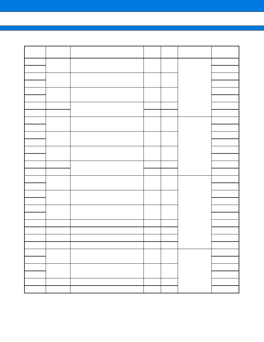
PRODUCT LINEUP
(Continued)
Item
Part number
MB90V460
MB90F462
MB90462
MB90467
Classification
Development/evaluation
product
Mass-produced
products
(Flash ROM)
Mass-produced products
(Mask ROM)
ROM size
64 KBytes
RAM size
8 KBytes
2 KBytes
CPU function
Number of Instruction : 351
Minimum execution time : 62.5 ns / 4 MHz (PLL
×
4)
Addressing mode : 23
Data bit length : 1, 8, 16 bits
Maximum memory space : 16 MBytes
I/O port
I/O port (CMOS) : 51
PWC
Pulse width counter timer : 2 channels
Pulse width counter
timer : 1ch
Timer function (select the counter timer from three internal clocks)
Various Pulse width measuring function (H pulse width, L pulse width, rising edge to fall-
ing edge period, falling edge to rising edge period, rising edge to rising edge period and
falling edge to falling edge period)
UART
UART : 2 channels
With full-duplex double buffer (8-bit length)
Clock asynchronized or clock synchronized transmission (with start and stop bits) can
be selectively used
Transmission can be one-to-one (bi-directional commuication) or one-to-n (Master-
Slave communication)
16-bit reload timer
Reload timer : 2 channels
Reload mode, single-shot mode or event count mode selectable
Can be worked with a multi-pulse generator or individually
16-bit PPG timer
PPG timer : 3 channels
PPG timer : 2ch
PWM mode or single-shot mode selectable
Can be worked with multi-functional timer / multi-pulse generator or individually
Multi-functional
timer
(for AC/DC
motor control)
16-bit free-running timer with up or up/down mode selection and buffer : 1 channel
16-bit output compare : 6 channels
16-bit input capture : 4 channels
16-bit PPG timer : 1 channel
Waveform generator (16-bit timer : 3 channels, 3-phase waveform or dead time)
Multi-pulse
generator
(for DC motor control)
16-bit PPG timer : 1 channel
16-bit reload timer operation (toggle output, one shot output select-
able)
Event counter function : 1 channel built-in
A waveform sequencer (includes 16-bit timer with buffer and com-
pare clear function)
8/10-bit A/D
converter
8/10-bit resolution (8 channels)
Conversion time : Less than 6.13
µ
S (16 MHz internal clock)
DTP/External
interrupt
8 independent channels
Selectable causes : Rising edge, falling edge, "L" level or "H" level
Lower power
consumption
Stop mode / Sleep mode / CPU intermittent operation mode
MB90460 Series
5
(Continued)
* : Varies with conditions such as the operating frequency (See section "
s
ELECTRICAL CHARACTERISTICS") .
Assurance for the MB90V460 is given only for operation with a tool at a power supply voltage of 4.5 V to 5.5 V,
an operating temperature of 0 to
+
25
°
C, and an operating frequency of 1 MHz to 16 MHz.
s
s
s
s
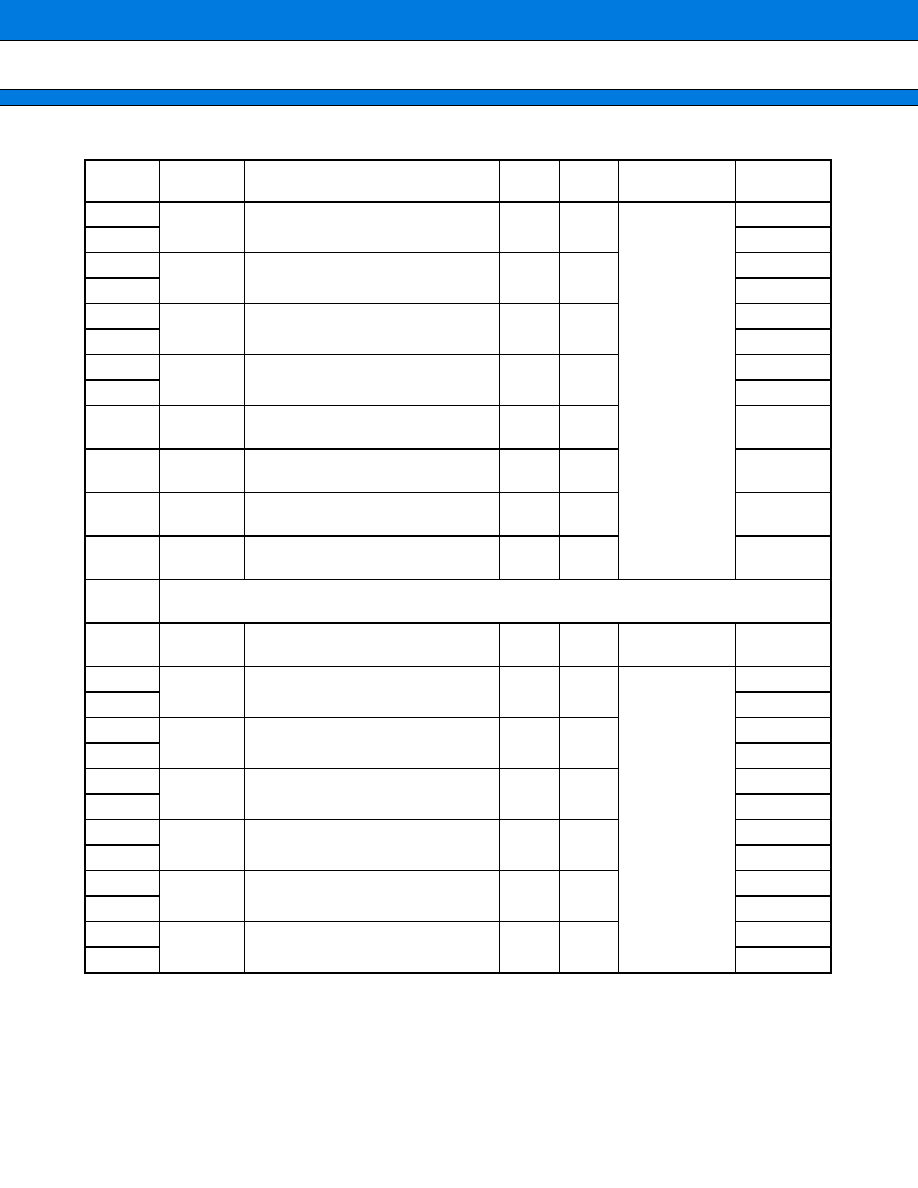
PACKAGE AND CORRESPONDING PRODUCTS
: Available,
: Not available
Note : For more information about each package, see section "
s
PACKAGE DIMENSIONS".
s
s
s
s
DIFFERENCES AMONG PRODUCTS
Memory Size
In evaluation with an evaluation product, note the difference between the evaluation product and the product
actually used. The following items must be taken into consideration.
· The MB90V460 does not have an internal ROM, however, operations equivalent to chips with an internal ROM
can be evaluated by using a dedicated development tool, enabling selection of ROM size by settings of the
development tool.
· In the MB90V460, images from FF4000
H
to FFFFFF
H
are mapped to bank 00, and FE0000
H
to FF3FFF
H
are
mapped to bank FF only. (This setting can be changed by configuring the development tool.)
· In the MB90462/F462/467, images from FF4000
H
to FFFFFF
H
are mapped to bank 00, and FF0000
H
to
FF3FFF
H
are mapped to bank FF only.
Item
Part number
MB90V460
MB90F462
MB90462
MB90467
Package PGA256
LQFP-64 (FPT-64P-M09 : 0.65 mm pitch)
QFP-64 (FPT-64P-M06 : 1.00 mm pitch)
SDIP-64 (DIP-64P-M01 : 1.78 mm pitch)
Power supply voltage for
operation*
4.5 V to 5.5 V *
Process
CMOS
Package
MB90V460
MB90F462
MB90462
MB90467
PGA256
FPT-64P-M09
FTP-64P-M06
DIP-64P-M01
×
×
×
×
×
×
×
MB90460 Series
6
s
s
s
s
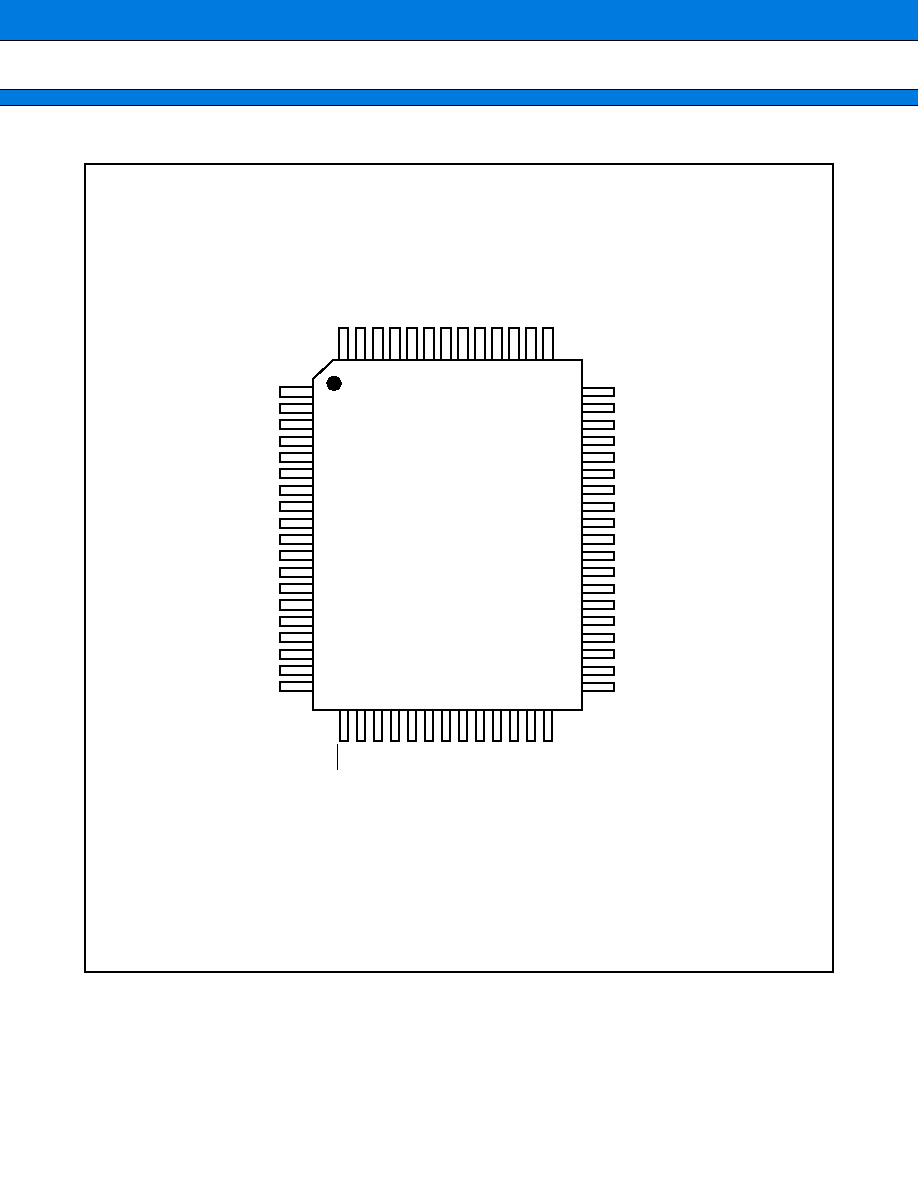
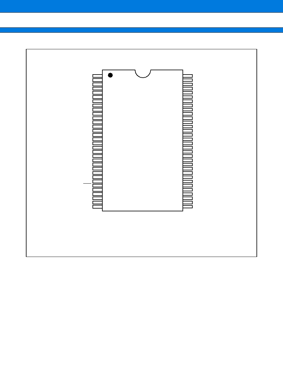
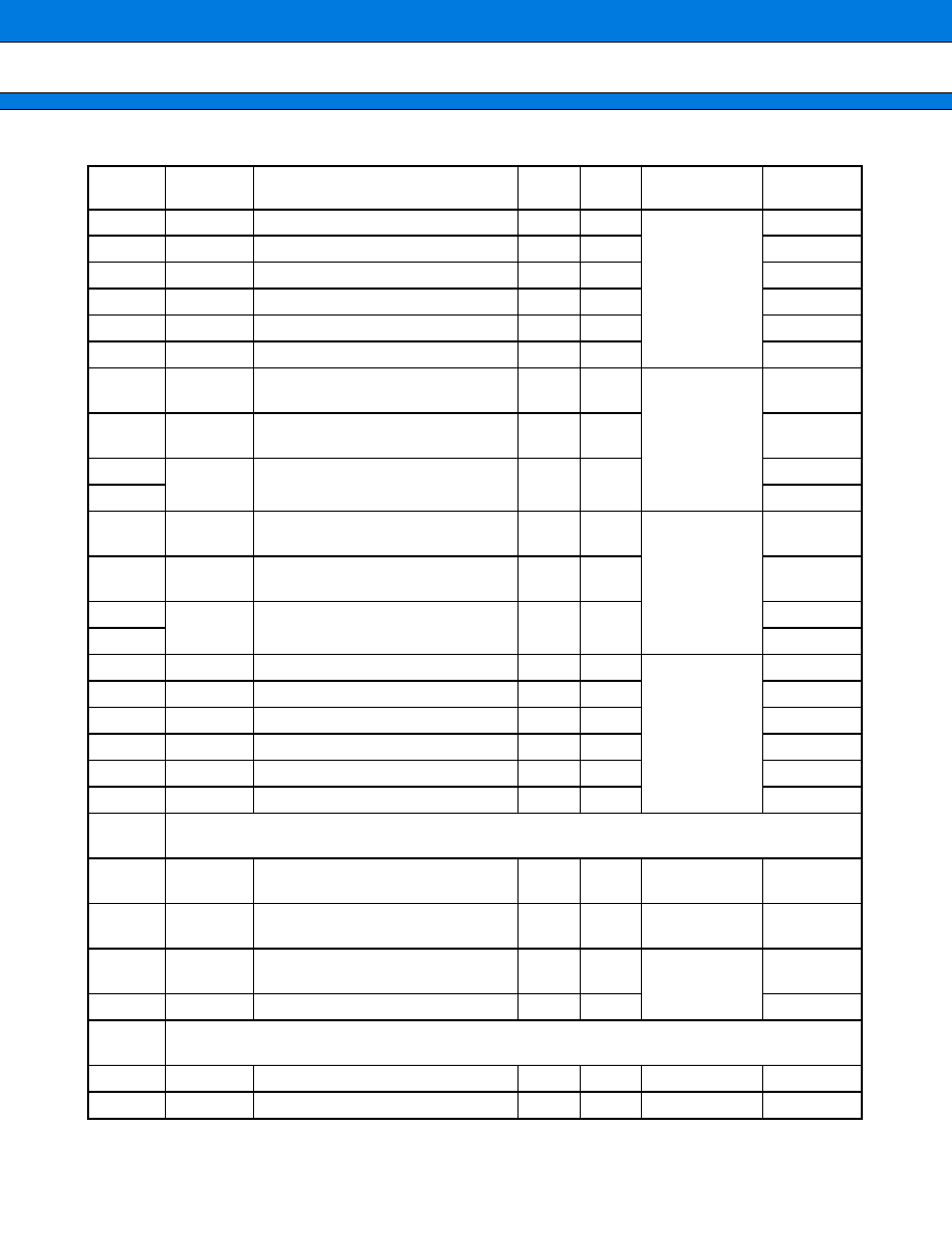
PIN ASSIGNMENT
(Continued)
(TOP VIEW)
(FPT-64P-M06)
*1 : Heavy current pins
*2 : MB90V460, MB90F462, MB90462 only.
They do not exist on MB90467, because there are not PWC (ch 0) , 16-bit PPG (ch 1) and waveform
sequencer.
P44/SNI1*
2
P45/SNI2*
2
P46/PPG2
P50/AN0
P51/AN1
P52/AN2
P53/AN3
P54/AN4
P55/AN5
P56/AN6
P57/AN7
AV
CC
AVR
AV
SS
P60/SIN1
P61/SOT1
P62/SCK1
P63/INT7
MD0
1
2
3
4
5
6
7
8
9
10
11
12
13
14
15
16
17
18
19
51
50
49
48
47
46
45
44
43
42
41
40
39
38
37
36
35
34
33
P30*
1
/RTO0 (U)
V
SS
P27/IN3
P26/IN2
P25/IN1
P24/IN0
P23/PWO1
P22/PWI1
P21/TO1
P20/TIN1
P17/FRCK
P16/INT6/TO0
P15/INT5/TIN0
P14/INT4
P13/INT3
P12/INT2/DTTI1*
2
P11/INT1
P10/INT0/DTTI0
P07/PWO0*
2
64
63
62
61
60
59
58
57
56
55
54
53
52
P43/SNI0*
2
P42/SCK0
P41/SO
T0
P40/SIN0
P37/PPG0
P36/PPG1*
2
C
V
CC
P35*
1
/R
T
O5 (Z)
P34*
1
/R
T
O4 (W)
P33*
1
/R
T
O3 (Y)
P32*
1
/R
T
O2 (V)
P31*
1
/R
T
O1 (X)
20
21
22
23
24
25
26
27
28
29
30
31
32
RST
MD1
MD2
X0
X1
V
SS
P00*
1
/OPT0*
2
P01*
1
/OPT1*
2
P02*
1
/OPT2*
2
P03*
1
/OPT3*
2
P04*
1
/OPT4*
2
P05*
1
/OPT5*
2
P06/PWI0*
2
MB90460 Series
7
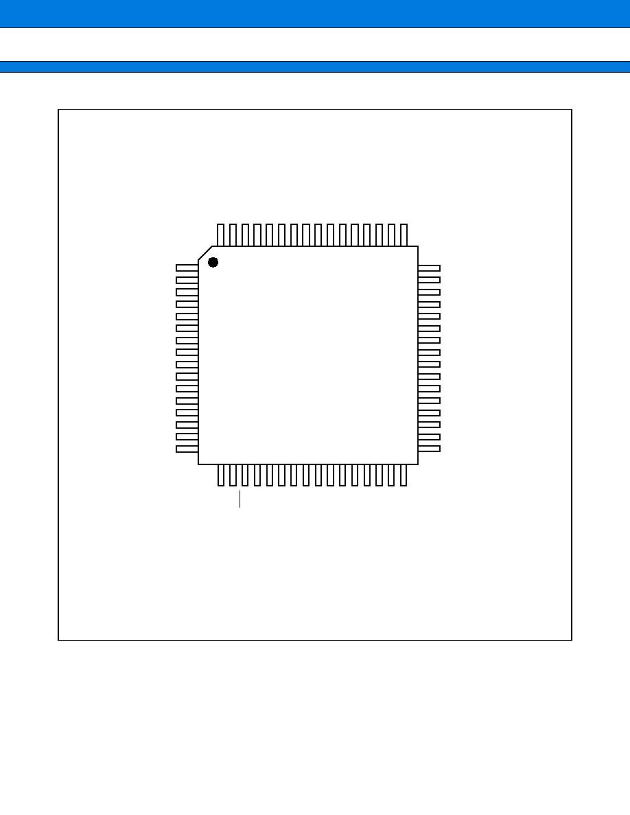
(Continued)
(TOP VIEW)
(FPT-64P-M09)
*1 : Heavy current pins
*2 : MB90V460, MB90F462, MB90462 only.
They do not exist on MB90467, because there are not PWC (ch 0) , 16-bit PPG (ch 1) and waveform
sequencer.
P45/SNI2*
2
P46/PPG2
P50/AN0
P51/AN1
P52/AN2
P53/AN3
P54/AN4
P55/AN5
P56/AN6
P57/AN7
AV
CC
AVR
AV
SS
P60/SIN1
P61/SOT1
P62/SCK1
1
2
3
4
5
6
7
8
9
10
11
12
13
14
15
16
48
47
46
45
44
43
42
41
40
39
38
37
36
35
34
33
P27/IN3
P26/IN2
P25/IN1
P24/IN0
P23/PWO1
P22/PWI1
P21/TO1
P20/TIN1
P17/FRCK
P16/INT6/TO0
P15/INT5/TIN0
P14/INT4
P13/INT3
P12/INT2/DTTI1*
2
P11/INT1
P10/INT0/DTTI0
64
63
62
61
60
59
58
57
56
55
54
53
52
51
50
49
P44/SNI1*
2
P43/SNI0*
2
P42/SCK0
P41/SO
T0
P40/SIN0
P37/PPG0
P36/PPG1*
2
C
V
CC
P35*
1
/R
T
O5 (Z)
P34*
1
/R
T
O4 (W)
P33*
1
/R
T
O3 (Y)
P32*
1
/R
T
O2 (V)
P31*
1
/R
T
O1 (X)
P30*
1
/R
T
O0 (U)
V
SS
17
18
19
20
21
22
23
24
25
26
27
28
29
30
31
32
P63/INT7
MD0
RST
MD1
MD2
X0
X1
V
SS
P00*
1
/OPT0*
2
P01*
1
/OPT1*
2
P02*
1
/OPT2*
2
P03*
1
/OPT3*
2
P04*
1
/OPT4*
2
P05*
1
/OPT5*
2
P06/PWI0
P07/PW
O0
MB90460 Series
8
(Continued)
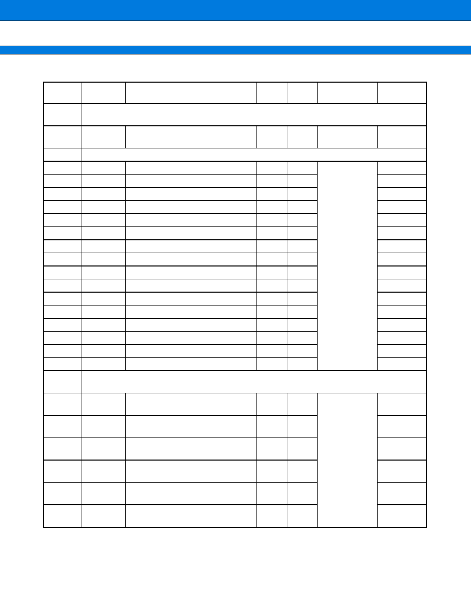
(TOP VIEW)
(DIP-64P-M01)
*1 : Heavy current pins
*2 : MB90V460, MB90F462, MB90462 only.
They do not exist on MB90467, because there are not PWC (ch 0) , 16-bit PPG (ch 1) and waveform
sequencer.
C
P36/PPG1*
2
P37/PPG0
P40/SIN0
P41/SOT0
P42/SCK0
P43/SNI0*
2
P44/SNI1*
2
P45/SNI2*
2
P46/PPG2
P50/AN0
P51/AN1
P52/AN2
P53/AN3
P54/AN4
P55/AN5
P56/AN6
P57/AN7
AV
CC
AVR
AV
SS
P60/SIN1
P61/SOT1
P62/SCK1
P63/INT7
MD0
RST
MD1
MD2
X0
X1
V
SS
1
2
3
4
5
6
7
8
9
10
11
12
13
14
15
16
17
18
19
20
21
22
23
24
25
26
27
28
29
30
31
32
64
63
62
61
60
59
58
57
56
55
54
53
52
51
50
49
48
47
46
45
44
43
42
41
40
39
38
37
36
35
34
33
V
CC
P35*
1
/RTO5 (Z)
P34*
1
/RTO4 (W)
P33*
1
/RTO3 (Y)
P32*
1
/RTO2 (V)
P31*
1
/RTO1 (X)
P30*
1
/RTO0 (U)
V
SS
P27/IN3
P26/IN2
P25/IN1
P24/IN0
P23/PWO1
P22/PWI1
P21/TO1
P20/TIN1
P17/FRCK
P16/INT6/TO0
P15/INT5/TIN0
P14/INT4
P13/INT3
P12/INT2/DTTI1*
2
P11/INT1
P10/INT0/DTTI0
P07/PWO0*
2
P06/PWI0*
2
P05*
1
/OPT5*
2
P04*
1
/OPT4*
2
P03*
1
/OPT3*
2
P02*
1
/OPT2*
2
P01*
1
/OPT1*
2
P00*
1
/OPT0*
2
MB90460 Series
9
s
s
s
s
PIN DESCRIPTION
(Continued)
Pin No.
Pin
name
I/O
circuit
Function
QFP-
M06*
2
LQFP-
M09*
1
SDIP*
3
23, 24
22, 23
30, 31
X0, X1
A
Oscillation input pins.
20
19
27
RST
B
External reset input pin.
26 to
31
25 to
30
33 to
38
P00 to
P05
D
General-purpose I/O ports.
OPT0 to
OPT5*
4
Output terminals OPT0 to 5 of the waveform sequencer.
These pins output the waveforms specified at the output data
registers of the waveform sequencer circuit. Output is generated
when OPE0 to 5 of OPCR is enabled.*
4
32
31
39
P06
E
General-purpose I/O ports.
PWI0*
4
PWC 0 signal input pin.*
4
33
32
40
P07
E
General-purpose I/O ports.
PWO0*
4
PWC 0 signal output pin.*
4
34
33
41
P10
C
General-purpose I/O ports.
INT0
Can be used as interrupt request input channels 0. Input is en-
abled when 1 is set in EN0 in standby mode.
DTTI0
RTO0 to 5 pins for fixed-level input. This function is enabled
when the waveform generator enables its input bits.
35
34
42
P11
C
General-purpose I/O ports.
INT1
Can be used as interrupt request input channels 1. Input is en-
abled when 1 is set in EN1 in standby mode.
36
35
43
P12
C
General-purpose I/O ports.
INT2
Can be used as interrupt request input channels 2. Input is en-
abled when 1 is set in EN2 in standby mode.
DTTI1*
4
OPT0 to 5 pins for fixed-level input. This function is enabled
when the waveform sequencer enables its input bit.*
4
37 to
38
36 to
37
44 to
45
P13 to
P14
C
General-purpose I/O ports.
INT3 to
INT4
Can be used as interrupt request input channels 3 to 4.
Input is enabled when 1 is set in EN3 to EN4 in standby mode.
39
38
46
P15
C
General-purpose I/O ports.
INT5
Can be used as interrupt request input channel 5. Input is en-
abled when 1 is set in EN5 in standby mode.
TIN0
External clock input pin for reload timer 0.
MB90460 Series
10
Pin No.
Pin
name
I/O
circuit
Function
QFP-
M06*
2
LQFP-
M09*
1
SDIP*
3
40
39
47
P16
C
General-purpose I/O ports.
INT6
Can be used as interrupt request input channels 6. Input is en-
abled when 1 is set in EN6 in standby mode.
TO0
Event output pin for reload timer 0.
41
40
48
P17
C
General-purpose I/O ports.
FRCK
External clock input pin for free-running timer.
42
41
49
P20
F
General-purpose I/O ports.
TIN1
External clock input pin for reload timer 1.
43
42
50
P21
F
General-purpose I/O ports.
TO1
Event output pin for reload timer 1.
44
43
51
P22
F
General-purpose I/O ports.
PWI1
PWC 1 signal input pin.
45
44
52
P23
F
General-purpose I/O ports.
PWO1
PWC 1 signal output pin.
46 to
49
45 to
48
53 to
56
P24 to
P27
F
General-purpose I/O ports.
IN0 to
IN3
Trigger input pins for input capture channels 0 to 3.
When input capture channels 0 to 3 are used for input operation,
these pins are enabled as required and must not be used for any
other I/P.
51 to
56
50 to
55
58 to
63
P30 to
P35
G
General-purpose I/O ports.
RTO0 (U)
to
RTO5 (Z)
Waveform generator output pins. These pins output the wave-
forms specified at the waveform generator. Output is generated
when waveform generator output is enabled. (U) to (Z) show the
coils that control 3-phase motor.
59
58
2
P36
H
General-purpose I/O ports.
PPG1*
4
Output pins for PPG channels 1. This function is enabled when
PPG channels 1 enable output.*
4
60
59
3
P37
H
General-purpose I/O ports.
PPG0
Output pins for PPG channels 0. This function is enabled when
PPG channels 0 enable output.
61
60
4
P40
F
General-purpose I/O ports.
SIN0
Serial data input pin for UART channel 0. While UART channel
0 is operating for input, the input of this pin is used as required
and must not be used for any other input.
62
61
5
P41
F
General-purpose I/O ports.
SOT0
Serial data output pin for UART channel 0. This function is en-
abled when UART channel 0 enables data output.
MB90460 Series
11
(Continued)
(Continued)
(Continued)
Pin No.
Pin
name
I/O
circuit
Function
QFP-
M06*
2
LQFP-
M09*
1
SDIP*
3
63
62
6
P42
F
General-purpose I/O ports.
SCK0
Serial clock I/O pin for UART channel 0. This function is enabled
when UART channel 0 enables clock output.
64
63
7
P43
F
General-purpose I/O ports.
SNI0*
4
Trigger input pins for position detection of the waveform se-
quencer. When this pin is used for input operation, it is enabled
as required and must not be used for any other I/P.*
4
1
64
8
P44
F
General-purpose I/O ports.
SNI1*
4
Trigger input pins for position detection of the Multi-pulse gener-
ator. When this pin is used for input operation, it is enabled as
required and must not be used for any other I/P.*
4
2
1
9
P45
F
General-purpose I/O ports.
SNI2*
4
Trigger input pins for position detection of the Multi-pulse gener-
ator. When this pin is used for input operation, it is enabled as
required and must not be used for any other I/P.*
4
3
2
10
P46
F
General-purpose I/O ports.
PPG2
Output pins for PPG channel 2. This function is enabled when
PPG channel 2 enables output.
4 to 11
3 to 10
11 to
18
P50 to
P57
I
General-purpose I/O ports.
AN0 to
AN7
A/D converter analog input pins. This function is enabled when
the analog input specification is enabled. (ADER) .
12
11
19
AV
CC
V
CC
power input pin for analog circuits.
13
12
20
AVR
Reference voltage (
+
) input pin for the A/D converter. This volt-
age must not exceed V
CC
and AV
CC
. Reference voltage (
-
) is
fixed to AV
SS
.
14
13
21
AV
SS
V
SS
power input pin for analog circuits.
15
14
22
P60
F
General-purpose I/O ports.
SIN1
Serial data input pin for UART channel 1. While UART channel
1 is operating for input, the input of this pin is used as required
and must not be used for any other in-put.
16
15
23
P61
F
General-purpose I/O ports.
SOT1
Serial data output pin for UART channel 1. This function is en-
abled when UART channel 1 enables data output.
MB90460 Series
12
(Continued)
*1 : FPT-64P-M09
*2 : FPT-64P-M06
*3 : DIP-64P-M01
*4 : MB90V460, MB90F462, MB90462 only.
They do not exist on MB90467, because there are not PWC (ch 0) , 16-bit PPG (ch 1) and waveform sequencer.
Pin No.
Pin
name
I/O
circuit
Function
QFP-
M06*
2
LQFP-
M09*
1
SDIP*
3
17
16
24
P62
F
General-purpose I/O port.
SCK1
Serial clock I/O pin for UART channel 1. This function is enabled
when UART channel 1 enables clock output.
18
17
25
P63
F
General-purpose I/O port.
INT7
Usable as interrupt request input channel 7. Input is enabled
when 1 is set in EN7 in standby mode.
19
18
26
MD0
J
Input pin for operation mode specification. Connect this pin di-
rectly to V
CC
or V
SS
.
21, 22
20, 21
28, 29
MD1,
MD2
J
Input pin for operation mode specification. Connect this pin di-
rectly to V
CC
or V
SS
.
25, 50
24, 49
32, 57
V
SS
Power (0 V) input pin.
57
56
64
V
CC
Power (5 V) input pin.
58
57
1
C
Capacity pin for power stabilization. Please connect to an ap-
proximately 0.1
µ
F ceramic capacitor.
MB90460 Series
13
s
s
s
s
I/O CIRCUIT TYPE
(Continued)
Classification
Type
Remarks
A
Main clock (main clock crystal
oscillator)
· At an oscillation feedback
resistor of approximately
1 M
B
· Hysteresis input
· Pull-up resistor
approximately 50 k
C
· CMOS output
· Hysteresis input
· Selectable pull-up resistor
approximately 50 k
· I
OL
=
4 mA
· Standby control available
D
· CMOS output
· CMOS input
· Selectable pull-up resistor
approximately 50 k
· Standby control available
· I
OL
=
12 mA
X1
Xout
X0
N-ch P-ch
N-ch
P-ch
Standby mode control
R
R
Pout
P-ch
Pull up control
Hysteresis input
Standby mode control
P-ch
N-ch
Nout
R
Pout
P-ch
Pull up control
CMOS input
Standby mode control
P-ch
N-ch
Nout
MB90460 Series
14
(Continued)
Classification
Type
Remarks
E
· CMOS output
· CMOS input
· Selectable pull-up resistor
approximately 50 k
· Standby control available
· I
OL
=
4 mA
F
· CMOS output
· Hysteresis input
· Standby control available
· I
OL
=
4 mA
G
· CMOS output
· CMOS input
· Standby control available
· I
OL
=
12 mA
H
· CMOS output
· CMOS input
· Standby control available
· I
OL
=
4 mA
R
Pout
P-ch
Pull up control
CMOS input
Standby mode control
P-ch
N-ch
Nout
Pout
Hysteresis input
Standby mode control
P-ch
N-ch
Nout
Pout
CMOS input
Standby mode control
P-ch
N-ch
Nout
Pout
CMOS input
Standby mode control
P-ch
N-ch
Nout

MB90460 Series
15
(Continued)
Classification
Type
Remarks
I
· CMOS output
· CMOS input
· Analog input
· I
OL
=
4 mA
J
· Hysteresis input
Pout
CMOS input
Analog input control
Analog input
P-ch
N-ch
Nout
MB90460 Series
16
s
s
s
s
HANDLING DEVICES
1.
Preventing Latchup
CMOS ICs may cause latchup in the following situations :
· When a voltage higher than V
CC
or lower than V
SS
is applied to input or output pins.
· When a voltage exceeding the rating is applied between V
CC
and V
SS
.
· When AV
CC
power is supplied prior to the V
CC
voltage.
If latchup occurs, the power supply current increases rapidly, sometimes resulting in thermal breakdown of the
device. Use meticulous care not to let it occur.
For the same reason, also be careful not to let the analog power-supply voltage exceed the digital power-supply
voltage.
2.
Handling unused input pins
Unused input pins left open may cause abnormal operation, or latch-up leading to permanent damage. Unused
input pins should be pulled up or pulled down through at least 2 k
resistance.
Unused input/output pins may be left open in the output state, but if such pins are in the input state they should
be handled in the same way as input pins.
3.
Use of the external clock
When the device uses an external clock, drive only the X0 pin while leaving the X1 pin open (See the illustration
below) .
4.
Power Supply Pins (V
CC
/V
SS
)
In products with multiple V
CC
or V
SS
pins, the pins of a same potential are internally connected in the device to
avoid abnormal operations including latch-up. However, connect the pins external power and ground lines to
lower the electro-magnetic emission level to prevent abnormal operation of strobe signals caused by the rise in
the ground level, and to conform to the total current rating.
Make sure to connect V
CC
and V
SS
pins via the lowest impedance to power lines.
It is recommended to provide a bypass capacitor of around 0.1
µ
F between V
CC
and V
SS
pins near the device.
5.
Crystal Oscillator Circuit
Noise around X0 or X1 pins may cause abnormal operations. Make sure to provide bypass capacitors via the
shortest distance from X0, X1 pins, crystal oscillator (or ceramic resonator) and ground lines, and make sure,
to the utmost effort, that lines of oscillation circuit not cross the lines of other circuits.
It is highly recommended to provide a printed circuit board art work surrounding X0 and X1 pins with the ground
area for stabilizing the operation.
6.
Turning-on Sequence of Power Supply to A/D Converter and Analog Inputs
Make sure to turn on the A/D converter power supply (AV
CC
, AV
SS
, AVR) and analog inputs (AN0 to AN7) after
turning-on the digital power supply (V
CC
) .
Turn-off the digital power after turning off the A/D converter supply and analog inputs. In this case, make sure
that the voltage of AVR dose not exceed AV
CC
(turning on/off the analog and digital power supplies simultaneously
is acceptable) .
X0
X1
Open
MB90460 series

MB90460 Series
17
7.
Connection of Unused Pins of A/D Converter
Connect unused pin of A/D converter to AV
CC
=
V
CC
, AV
SS
=
AVR
=
V
SS
.
8.
N.C. Pin
The N.C. (internally connected) pin must be opened for use.
9.
Notes on Energization
To prevent the internal regulator circuit from malfunctioning, set the voltage rise time during energization at 50
µ
s or more.
10. Initialization
In the device, there are internal registers which are initialized only by a power-on reset. To initialize these registers,
please turn on the power again.
11. Return from standby state
If the power-supply voltage goes below the standby RAM holding voltage in the standby state, the device may
fail to return from the standby state. In this case, reset the device via the external reset pin to return to the normal
state.
MB90460 Series
18
s
s
s
s
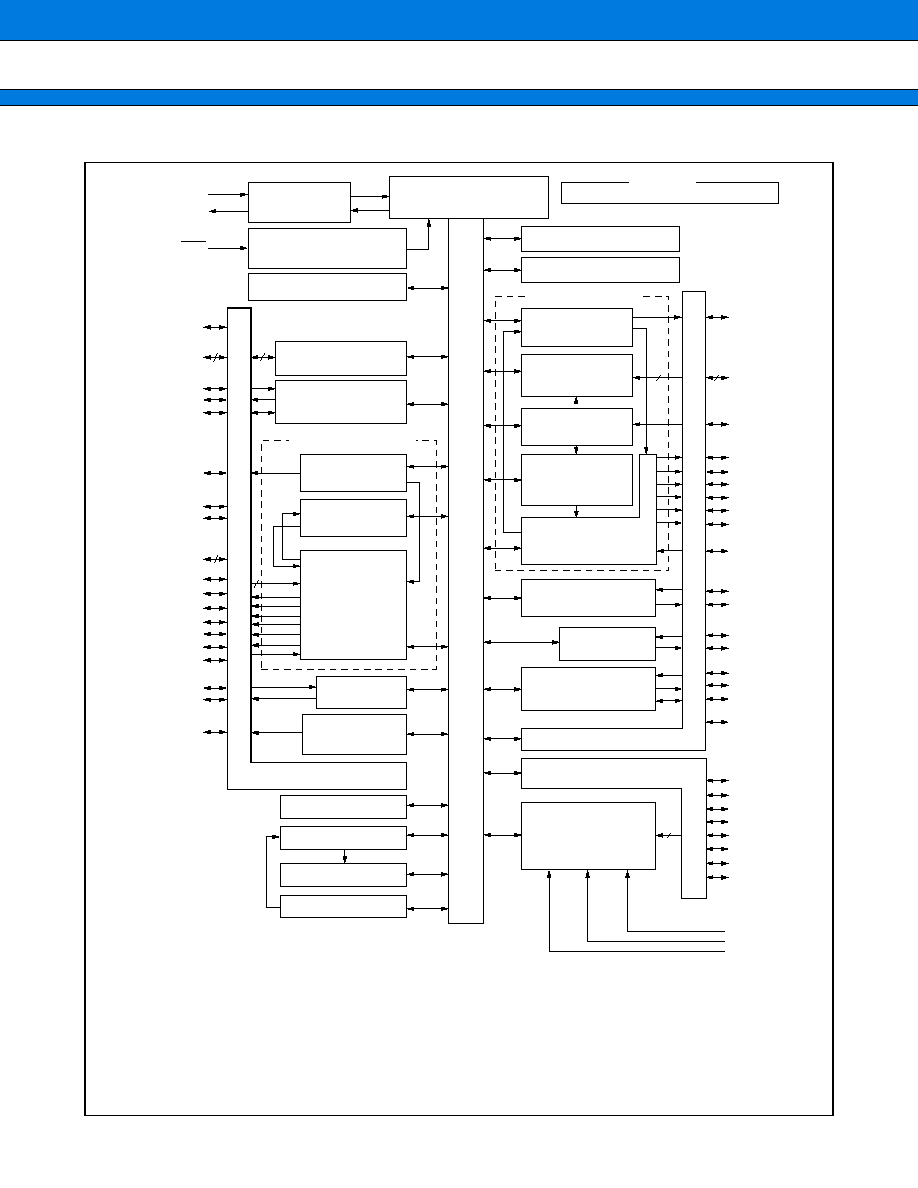
BLOCK DIAGRAM
X0
X1
RST
P11/INT1
P40/SIN0
P41/SOT0
P42/SCK0
P36/PPG1
2
P15/INT5/TIN0
P16/INT6/TO0
P00/OPT0
2
P01/OPT1
2
P02/OPT2
2
P03/OPT3
2
P04/OPT4
2
P05/OPT5
2
P06/PWI0
2
P07/PWO0
2
P46/PPG2
P12/INT2/DTTI1
2
P43/SNI0
2
to
P45/SNI2
2
P13/INT3 to
P14/INT4
2
3
Clock control
circuit
Reset circuit
(Watch-dog timer)
Interrupt controller
DTP/External interrupt
UART
(Ch0)
16-bit PPG
(Ch1)
16-bit reload timer
(Ch0)
Waveform
sequencer
Multi-pulse Generator
3
8
PWC
(Ch0)
16-bit PPG
(Ch2)
CMOS I/O port 0, 1, 3, 4
RAM
ROM
ROM correction
ROM mirroring
F
2
MC-16LX Bus
CPU
F
2
MC-16LX series core
Other pins
V
SS
×
2, V
CC
×
1, MD0-2, C
Timebase timer
Delayed interrupt generator
Multi-functional Timer
4
4
16-bit PPG
(Ch0)
16-bit input capture
(Ch0/1/2/3)
16-bit free-run
timer
16-bit output
compare
(Ch0 to 5)
Waveform
generator
16-bit reload timer
(Ch1)
PWC
(Ch1)
UART
(Ch1)
CMOS I/O port 1, 2, 3, 6
CMOS I/O port 5
A/D converter
(8/10 bit)
P37/PPG0
P17/FRCK
P30/RTO0 (U)
P31/RTO1 (X)
P32/RTO2 (V)
P33/RTO3 (Y)
P34/RTO4 (W)
P35/RTO5 (Z)
P10/INT0/DTTI0
P20/TIN1
P22/PWI1
P23/PWO1
P60/SIN1
P61/SOT1
P62/SCK1
P63/INT7
P50/AN0
P51/AN1
P52/AN2
P53/AN3
P54/AN4
P55/AN5
P56/AN6
P57/AN7
AV
CC
AVR
AV
SS
P21/TO1
P24/IN0 to
P27/IN3
8
1
1
1
2
Note : P00 to P07 (8 channels) : With registers that can be used
as input pull-up resistors
P10 to P17 (8 channels) : With registers that can be used as input pull-up resistors
*1: Only MB90V460, MB90F462 and MB90462 have PWC (ch 0) , 16-bit PPG (ch 1) and waveform sequencer.
They do not exist on MB90467.
*2: The multi-pulse generator function can be used only by MB90V460, MB90F462 and MB90462.
This function can not be used by MB90467.
MB90460 Series
19
s
s
s
s
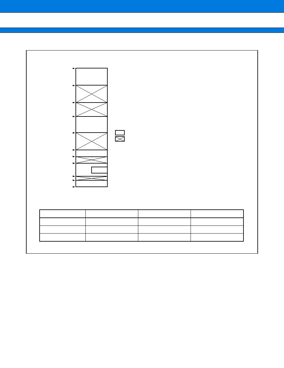
MEMORY MAP
Note : The ROM data of bank FF is reflected in the upper address of bank 00, realizing effective use of the C
compiler small model. The lower 16-bit is assigned to the same address, enabling reference of the table on
the ROM without stating "far". For example, if an attempt has been made to access 00C000
H
, the contents
of the ROM at FFC000
H
are accessed actually. Since the ROM area of the FF bank exceeds 48 Kbytes, the
whole area cannot be reflected in the image for the 00 bank. The ROM data at FF4000
H
to FFFFFF
H
looks,
therefore, as if it were the image for 004000
H
to 00FFFF
H
. Thus, it is recommended that the ROM data table
be stored in the area of FF4000
H
to FFFFFF
H
.
FFFFFF
H
Address #1
Address #2
Address #3
FC0000
H
010000
H
004000
H
003FE0
H
000100
H
0000C0
H
000000
H
ROM area
Register
ROM area
(FF bank image)
Peripheral area
Peripheral area
RAM
area
: Internal access memory
: Access not allowed
In Single chip mode
the mirror function
is supported
Parts No.
Address#1
Address#2
Address#3
MB90462/467
FF0000
H
004000
H
000900
H
MB90F462
FF0000
H
004000
H
000900
H
MB90V460
(FF0000
H
) 004000
H
002100
H
MB90460 Series
20
s
s
s
s
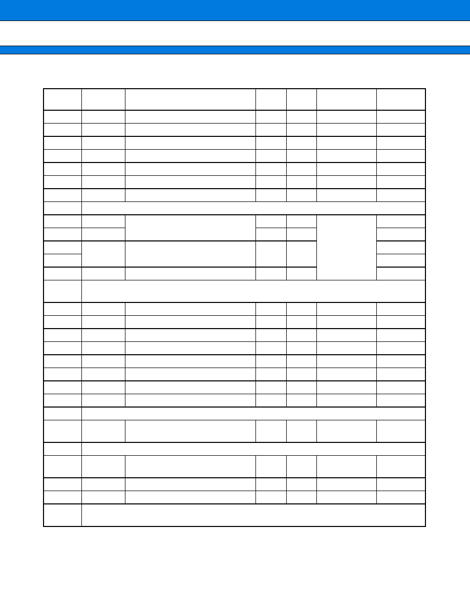
I/O MAP
(Continued)
Address
Abbrevia-
tion
Register
Byte
access
Word
access
Resource
name
Initial value
000000
H
PDR0
Port 0 data register
R/W
R/W
Port 0
XXXXXXXX
B
000001
H
PDR1
Port 1 data register
R/W
R/W
Port 1
XXXXXXXX
B
000002
H
PDR2
Port 2 data register
R/W
R/W
Port 2
XXXXXXXX
B
000003
H
PDR3
Port 3 data register
R/W
R/W
Port 3
XXXXXXXX
B
000004
H
PDR4
Port 4 data register
R/W
R/W
Port 4
-XXXXXXX
B
000005
H
PDR5
Port 5 data register
R/W
R/W
Port 5
XXXXXXXX
B
000006
H
PDR6
Port 6 data register
R/W
R/W
Port 6
----XXXX
B
000007
H
Prohibited area
000008
H
PWCSL0
PWC control status register CH0
R/W
R/W
PWC timer
(CH0)
00000000
B
000009
H
PWCSH0
R/W
R/W
00000000
B
00000A
H
PWC0
PWC data buffer register CH0
R/W
XXXXXXXX
B
00000B
H
XXXXXXXX
B
00000C
H
DIV0
Divide ratio control register CH0
R/W
R/W
------00
B
00000D
H
to 0F
H
Prohibited area
000010
H
DDR0
Port 0 direction register
R/W
R/W
Port 0
00000000
B
000011
H
DDR1
Port 1 direction register
R/W
R/W
Port 1
00000000
B
000012
H
DDR2
Port 2 direction register
R/W
R/W
Port 2
00000000
B
000013
H
DDR3
Port 3 direction register
R/W
R/W
Port 3
00000000
B
000014
H
DDR4
Port 4 direction register
R/W
R/W
Port 4
-0000000
B
000015
H
DDR5
Port 5 direction register
R/W
R/W
Port 5
00000000
B
000016
H
DDR6
Port 6 direction register
R/W
R/W
Port 6
----0000
B
000017
H
ADER
Analog input enable register
R/W
R/W
Port 5, A/D
11111111
B
000018
H
Prohibited area
000019
H
CDCR0
Clock division control register 0
R/W
R/W
Communication
prescaler 0
0---0000
B
00001A
H
Prohibited area
00001B
H
CDCR1
Clock division control register 1
R/W
R/W
Communication
prescaler 1
0---0000
B
00001C
H
RDR0
Port 0 pull-up resistor setting register
R/W
R/W
Port 0
00000000
B
00001D
H
RDR1
Port 1 pull-up resistor setting register
R/W
R/W
Port 1
00000000
B
00001E
H
to 1F
H
Prohibited area
MB90460 Series
21
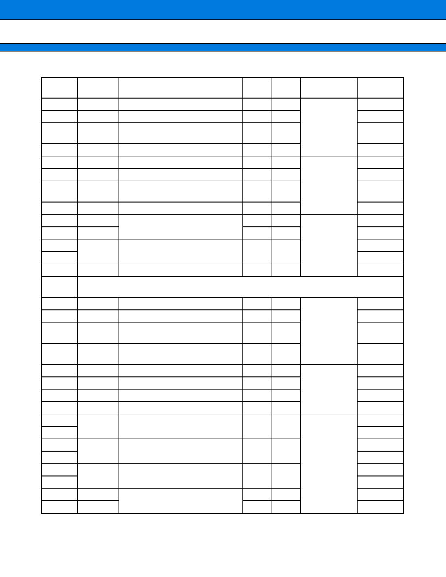
(Continued)
Address
Abbrevia-
tion
Register
Byte
access
Word
access
Resource
name
Initial value
000020
H
SMR0
Serial mode register 0
R/W
R/W
UART0
00000000
B
000021
H
SCR0
Serial control register 0
R/W
R/W
00000100
B
000022
H
SIDR0 /
SODR0
Input data register 0 /
output data register 0
R/W
R/W
XXXXXXXX
B
000023
H
SSR0
Serial status register 0
R/W
R/W
00001000
B
000024
H
SMR1
Serial mode register 1
R/W
R/W
UART1
00000000
B
000025
H
SCR1
Serial control register 1
R/W
R/W
00000100
B
000026
H
SIDR1 /
SODR1
Input data register 1 /
output data register 1
R/W
R/W
XXXXXXXX
B
000027
H
SSR1
Status register 1
R/W
R/W
00001000
B
000028
H
PWCSL1
PWC control status register CH1
R/W
R/W
PWC timer
(CH1)
00000000
B
000029
H
PWCSH1
R/W
R/W
00000000
B
00002A
H
PWC1
PWC data buffer register CH1
R/W
XXXXXXXX
B
00002B
H
XXXXXXXX
B
00002C
H
DIV1
Divide ratio control register CH1
R/W
R/W
------00
B
00002D
H
to 2F
H
Prohibited area
000030
H
ENIR
Interrupt / DTP enable register
R/W
R/W
DTP/external
interrupt
00000000
B
000031
H
EIRR
Interrupt / DTP cause register
R/W
R/W
XXXXXXXX
B
000032
H
ELVRL
Request level setting register
(Lower Byte)
R/W
R/W
00000000
B
000033
H
ELVRH
Request level setting register
(Higher Byte)
R/W
R/W
00000000
B
000034
H
ADCS0
A/D control status register 0
R/W
R/W
8/10-bit A/D
converter
00000000
B
000035
H
ADCS1
A/D control status register 1
R/W
R/W
00000000
B
000036
H
ADCR0
A/D data register 0
R
R
XXXXXXXX
B
000037
H
ADCR1
A/D data register 1
R/W
R/W
00000-XX
B
000038
H
PDCR0
PPG0 down counter register
R
16-bit
PPG timer
(CH0)
11111111
B
000039
H
11111111
B
00003A
H
PCSR0
PPG0 period setting register
W
XXXXXXXX
B
00003B
H
XXXXXXXX
B
00003C
H
PDUT0
PPG0 duty setting register
W
XXXXXXXX
B
00003D
H
XXXXXXXX
B
00003E
H
PCNTL0
PPG0 control status register
R/W
R/W
--000000
B
00003F
H
PCNTH0
R/W
R/W
00000000
B
MB90460 Series
22
(Continued)
Address
Abbrevia-
tion
Register
Byte
access
Word
access
Resource
name
Initial value
000040
H
PDCR1
PPG1 down counter register
R
16-bit
PPG timer
(CH1)
11111111
B
000041
H
11111111
B
000042
H
PCSR1
PPG1 period setting register
W
XXXXXXXX
B
000043
H
XXXXXXXX
B
000044
H
PDUT1
PPG1 duty setting register
W
XXXXXXXX
B
000045
H
XXXXXXXX
B
000046
H
PCNTL1
PPG1 control status register
R/W
R/W
--000000
B
000047
H
PCNTH1 R/W
R/W
00000000
B
000048
H
PDCR2
PPG2 down counter register
R
16-bit
PPG timer
(CH2)
11111111
B
000049
H
11111111
B
00004A
H
PCSR2
PPG2 period setting register
W
XXXXXXXX
B
00004B
H
XXXXXXXX
B
00004C
H
PDUT2
PPG2 duty setting register
W
XXXXXXXX
B
00004D
H
XXXXXXXX
B
00004E
H
PCNTL2
PPG2 control status register
R/W
R/W
--000000
B
00004F
H
PCNTH2
R/W
R/W
00000000
B
000050
H
TMRR0
16-bit timer register 0
R/W
Waveform
generator
XXXXXXXX
B
000051
H
XXXXXXXX
B
000052
H
TMRR1
16-bit timer register 1
R/W
XXXXXXXX
B
000053
H
XXXXXXXX
B
000054
H
TMRR2
16-bit timer register 2
R/W
XXXXXXXX
B
000055
H
XXXXXXXX
B
000056
H
DTCR0
16-bit timer control register 0
R/W
R/W
00000000
B
000057
H
DTCR1
16-bit timer control register 1
R/W
R/W
00000000
B
000058
H
DTCR2
16-bit timer control register 2
R/W
R/W
00000000
B
000059
H
SIGCR
Waveform control register
R/W
R/W
00000000
B
00005A
H
CPCLRB /
CPCLR
Compare clear buffer register /
Compare clear register (lower)
R/W
16-bit
free-running
timer
11111111
B
00005B
H
11111111
B
00005C
H
TCDT
Timer data register (lower)
R/W
00000000
B
00005D
H
00000000
B
00005E
H
TCCSL
Timer control status register (lower)
R/W
R/W
00000000
B
00005F
H
TCCSH
Timer control status register (upper)
R/W
R/W
-0000000
B
MB90460 Series
23
(Continued)
Address
Abbrevia-
tion
Register
Byte
access
Word
access
Resource
name
Initial value
000060
H
IPCP0
Input capture data register CH0
R
16-bit
input capture
(CH0 to CH3)
XXXXXXXX
B
000061
H
XXXXXXXX
B
000062
H
IPCP1
Input capture data register CH1
R
XXXXXXXX
B
000063
H
XXXXXXXX
B
000064
H
IPCP2
Input capture data register CH2
R
XXXXXXXX
B
000065
H
XXXXXXXX
B
000066
H
IPCP3
Input capture data register CH3
R
XXXXXXXX
B
000067
H
XXXXXXXX
B
000068
H
PICSL01
PPG output control / Input capture
control status register 01 (lower)
R/W
R/W
00000000
B
000069
H
PICSH01
PPG output control / Input capture
control status register 01 (upper)
R/W
R/W
00000000
B
00006A
H
ICSL23
Input capture control status register
23 (lower)
R/W
R/W 00000000
B
00006B
H
ICSH23
Input capture control status register
23 (upper)
R
R
------00
B
00006C
H
to 6E
H
Prohibited area
00006F
H
ROMM
ROM mirroring function selection
register
W
W
ROM mirroring
function
-------1
B
000070
H
OCCPB0/
OCCP0
Output compare buffer register /
output compare register 0
R/W
Output compare
(CH0 to CH5)
XXXXXXXX
B
000071
H
XXXXXXXX
B
000072
H
OCCPB1/
OCCP1
Output compare buffer register /
output compare register 1
R/W
XXXXXXXX
B
000073
H
XXXXXXXX
B
000074
H
OCCPB2/
OCCP2
Output compare buffer register /
output compare register 2
R/W
XXXXXXXX
B
000075
H
XXXXXXXX
B
000076
H
OCCPB3/
OCCP3
Output compare buffer register /
output compare register 3
R/W
XXXXXXXX
B
000077
H
XXXXXXXX
B
000078
H
OCCPB4/
OCCP4
Output compare buffer register /
output compare register 4
R/W
XXXXXXXX
B
000079
H
XXXXXXXX
B
00007A
H
OCCPB5/
OCCP5
Output compare buffer register /
output compare register 5
R/W
XXXXXXXX
B
00007B
H
XXXXXXXX
B
MB90460 Series
24
(Continued)
Address
Abbrevia-
tion
Register
Byte
access
Word
access
Resource
name
Initial value
00007C
H
OCS0
Compare control register 0
R/W
R/W
Output compare
(CH0 to CH5)
00000000
B
00007D
H
OCS1
Compare control register 1
R/W
R/W
-0000000
B
00007E
H
OCS2
Compare control register 2
R/W
R/W
00000000
B
00007F
H
OCS3
Compare control register 3
R/W
R/W
-0000000
B
000080
H
OCS4
Compare control register 4
R/W
R/W
00000000
B
000081
H
OCS5
Compare control register 5
R/W
R/W
-0000000
B
000082
H
TMCSRL0
Timer control status register CH0
(lower)
R/W
R/W
16-bit
reload timer
(CH0)
00000000
B
000083
H
TMCSRH0
Timer control status register CH0
(upper)
R/W
R/W
----0000
B
000084
H
TMR0 /
TMRD0
16 bit timer register CH0 /
16-bit reload register CH0
R/W
XXXXXXXX
B
000085
H
XXXXXXXX
B
000086
H
TMCSRL1
Timer control status register CH1
(lower)
R/W
R/W
16-bit reload
timer (CH1)
00000000
B
000087
H
TMCSRH1
Timer control status register CH1
(upper)
R/W
R/W
----0000
B
000088
H
TMR1 /
TMRD1
16 bit timer register CH1 /
16-bit reload register CH1
R/W
XXXXXXXX
B
000089
H
XXXXXXXX
B
00008A
H
OPCLR
Output control lower register
R/W
R/W
Waveform
sequencer
00000000
B
00008B
H
OPCUR
Output control upper register
R/W
R/W
00000000
B
00008C
H
IPCLR
Input control lower register
R/W
R/W
00000000
B
00008D
H
IPCUR
Input control upper register
R/W
R/W
00000000
B
00008E
H
TCSR
Timer control status register
R/W
R/W
00000000
B
00008F
H
NCCR
Noise cancellation control register
R/W
R/W
00000000
B
000090
H
to 9D
H
Prohibited area
00009E
H
PACSR
Program address detect control
status register
R/W
R/W
Rom correction
00000000
B
00009F
H
DIRR
Delayed interrupt cause /
clear register
R/W
R/W
Delayed
interrupt
-------0
B
0000A0
H
LPMCR
Low-power consumption mode
register
R/W
R/W
Low-power
consumption
control register
00011000
B
0000A1
H
CKSCR
Clock selection register
R/W
R/W
11111100
B
0000A2
H
to A7
H
Prohibited area
0000A8
H
WDTC
Watchdog control register
R/W
R/W
Watchdog timer
X-XXX111
B
0000A9
H
TBTC
Timebase timer control register
R/W
R/W
Timebase timer
1--00100
B
MB90460 Series
25
(Continued)
Address
Abbrevia-
tion
Register
Byte
access
Word
access
Resource
name
Initial value
0000AA
H
to AD
H
Prohibited area
0000AE
H
FMCS
Flash memory control status
register
R/W
R/W
Flash memory
interface circuit
00010000
B
0000AF
H
Prohibited area
0000B0
H
ICR00
Interrupt control register 00
R/W
R/W
Interrupt
controller
00000111
B
0000B1
H
ICR01
Interrupt control register 01
R/W
R/W
00000111
B
0000B2
H
ICR02
Interrupt control register 02
R/W
R/W
00000111
B
0000B3
H
ICR03
Interrupt control register 03
R/W
R/W
00000111
B
0000B4
H
ICR04
Interrupt control register 04
R/W
R/W
00000111
B
0000B5
H
ICR05
Interrupt control register 05
R/W
R/W
00000111
B
0000B6
H
ICR06
Interrupt control register 06
R/W
R/W
00000111
B
0000B7
H
ICR07
Interrupt control register 07
R/W
R/W
00000111
B
0000B8
H
ICR08
Interrupt control register 08
R/W
R/W
00000111
B
0000B9
H
ICR09
Interrupt control register 09
R/W
R/W
00000111
B
0000BA
H
ICR10
Interrupt control register 10
R/W
R/W
00000111
B
0000BB
H
ICR11
Interrupt control register 11
R/W
R/W
00000111
B
0000BC
H
ICR12
Interrupt control register 12
R/W
R/W
00000111
B
0000BD
H
ICR13
Interrupt control register 13
R/W
R/W
00000111
B
0000BE
H
ICR14
Interrupt control register 14
R/W
R/W
00000111
B
0000BF
H
ICR15
Interrupt control register 15
R/W
R/W
00000111
B
0000C0
H
to FF
H
External area
001FF0
H
PADR0L
Program address detection
register 0 (Lower Byte)
R/W
R/W
Rom correction
XXXXXXXX
B
001FF1
H
PADR0M
Program address detection
register 0 (Middle Byte)
R/W
R/W
XXXXXXXX
B
001FF2
H
PADR0H
Program address detection
register 0 (Higher Byte)
R/W
R/W
XXXXXXXX
B
001FF3
H
PADR1L
Program address detection
register 1 (Lower Byte)
R/W
R/W
XXXXXXXX
B
001FF4
H
PADR1M
Program address detection
register 1 (Middle Byte)
R/W
R/W
XXXXXXXX
B
001FF5
H
PADR1H
Program address detection
register 1 (Higher Byte)
R/W
R/W
XXXXXXXX
B
MB90460 Series
26
(Continued)
Address
Abbrevia-
tion
Register
Byte
access
Word
access
Resource
name
Initial value
003FE0
H
OPDBR0
Output data buffer register 0
R/W
Waveform
sequencer
00000000
B
003FE1
H
00000000
B
003FE2
H
OPDBR1
Output data buffer register 1
R/W
00000000
B
003FE3
H
00000000
B
003FE4
H
OPDBR2
Output data buffer register 2
R/W
00000000
B
003FE5
H
00000000
B
003FE6
H
OPDBR3
Output data buffer register 3
R/W
00000000
B
003FE7
H
00000000
B
003F78
H
OPDBR4
Output data buffer register 4
R/W
00000000
B
003FE9
H
00000000
B
003FEA
H
OPDBR5
Output data buffer register 5
R/W
00000000
B
003FEB
H
00000000
B
003FEC
H
OPEBR6
Output data buffer register 6
R/W
00000000
B
003FED
H
00000000
B
003FEE
H
OPEBR7
Output data buffer register 7
R/W
00000000
B
003FEF
H
00000000
B
003FF0
H
OPEBR8
Output data buffer register 8
R/W
00000000
B
003FF1
H
00000000
B
003FF2
H
OPEBR9
Output data buffer register 9
R/W
00000000
B
003FF3
H
00000000
B
003FF4
H
OPEBRA
Output data buffer register A
R/W
00000000
B
003FF5
H
00000000
B
003FF6
H
OPEBRB
Output data buffer register B
R/W
00000000
B
003FF7
H
00000000
B
003FF8
H
OPDR
Output data register
R
XXXXXXXX
B
003FF9
H
0000XXXX
B
003FFA
H
CPCR
Compare clear register
R/W
XXXXXXXX
B
003FFB
H
XXXXXXXX
B
003FFC
H
TMBR
Timer buffer register
R
00000000
B
003FFD
H
00000000
B
003FFE
H
to
003FFF
H
Prohibited area

MB90460 Series
27
· Meaning of abbreviations used for reading and writing
· Explanation of initial values
The Instruction using IO addressing e.g. MOV A, io, is not supported for registers area 003FE0
H
to 003FFF
H
.
Note : For bits that is initialized by an reset operation, the initial value set by the reset operation is listed as an initial
value. Note that the values are different from reading results.
For LPMCR/CKSCR/WDTC, there are cases where initialization is performed or not performed, depending
on the types of the reset. However, initial value for resets that initializes the value is listed.
R/W : Read and write enabled
R
: Read only
W
: Write only
0
: The bit is initialized to 0.
1
: The bit is initialized to 1.
X
: The initial value of the bit is undefined.
-
: The bit is not used. Its initial value is undefined.
MB90460 Series
28
s
s
s
s
INTERRUPT FACTORS, INTERRUPT VECTORS, INTERRUPT CONTROL REGISTER
(Continued)
Interrupt cause
EI
2
OS
support
Interrupt vector
Interrupt control
register
Priority
*2
Number
Address
ICR
Address
Reset
#08
08
H
FFFFDC
H
High
INT9 instruction
#09
09
H
FFFFD8
H
Exception processing
#10
0A
H
FFFFD4
H
A/D converter conversion termination
#11
0B
H
FFFFD0
H
ICR00
0000B0
H
*1
Output compare channel 0 match
#12
0C
H
FFFFCC
H
End of measurement by PWC0 timer /
PWC0 timer overflow
#13
0D
H
FFFFC8
H
ICR01
0000B1
H
*1
16-bit PPG timer 0
#14
0E
H
FFFFC4
H
Output compare channel 1 match
#15
0F
H
FFFFC0
H
ICR02
0000B2
H
*1
16-bit PPG timer 1
#16
10
H
FFFFBC
H
Output compare channel 2 match
#17
11
H
FFFFB8
H
ICR03
0000B3
H
*1
16-bit reload timer 1 underflow
#18
12
H
FFFFB4
H
Output compare channel 3 match
#19
13
H
FFFFB0
H
ICR04
0000B4
H
*1
DTP/ext. interrupt channels 0/1 detection
#20
14
H
FFFFAC
H
DTTI0
Output compare channel 4 match
#21
15
H
FFFFA8
H
ICR05
0000B5
H
*2
DTP/ext. interrupt channels 2/3 detection
#22
16
H
FFFFA4
H
DTTI1
Output compare channel 5 match
#23
17
H
FFFFA0
H
ICR06
0000B6
H
*1
End of measurement by PWC1 timer /
PWC1 timer overflow
#24
18
H
FFFF9C
H
DTP/ext. interrupt channels 4/5 detection
#25
19
H
FFFF98
H
ICR07
0000B7
H
*1
Waveform sequencer timer compare match
/ write timing
#26
1A
H
FFFF94
H
DTP/ext. interrupt channels 6/7 detection
#27
1B
H
FFFF90
H
ICR08
0000B8
H
*1
Waveform sequencer position detect /
compare interrupt
#28
1C
H
FFFF8C
H
Waveform generator 16-bit timer 0/1/2
underflow
#29
1D
H
FFFF88
H
ICR09
0000B9
H
*1
16-bit reload timer 0 underflow
#30
1E
H
FFFF84
H
16-bit free-running timer zero detect
#31
1F
H
FFFF80
H
ICR10 0000BA
H
*1
16-bit PPG timer 2
#32
20
H
FFFF7C
H
Input capture channels 0/1
#33
21
H
FFFF78
H
ICR11 0000BB
H
*1
16-bit free-running timer compare clear
#34
22
H
FFFF74
H
×
×
×
MB90460 Series
29
(Continued)
: Can be used and support the EI
2
OS stop request.
: Can be used and interrupt request flag is cleared by EI
2
OS interrupt clear signal.
: Cannot be used.
: Usable when an interrupt cause that shares the ICR is not used.
Interrupt cause
EI2OS
support
Interrupt vector
Interrupt control
register
Priority
*2
Number
Address
ICR
Address
Input capture channels 2/3
#35
23
H
FFFF70
H
ICR12 0000BC
H
*1
Timebase timer
#36
24
H
FFFF6C
H
UART1 receive
#37
25
H
FFFF68
H
ICR13 0000BD
H
*1
UART1 send
#38
26
H
FFFF64
H
UART0 receive
#39
27
H
FFFF60
H
ICR14 0000BE
H
*1
UART0 send
#40
28
H
FFFF5C
H
Flash memory status
#41
29
H
FFFF58
H
ICR15
0000BF
H
*1
Delayed interrupt generator module
#42
2A
H
FFFF54
H
Low
×

MB90460 Series
30
s
s
s
s
PERIPHERAL RESOURCES
1.
Low-Power Consumption Control Circuit
The MB90460 series has the following CPU operating mode configured by selection of an operating clock and
clock operation control.
· Clock mode
PLL clock mode : A PLL clock that is a multiple of the oscillation clock (HCLK) frequency is used to operate
the CPU and peripheral functions.
Main clock mode : The main clock, with a frequency one-half that of the oscillation clock (HCLK) , is used to
operate the CPU and peripheral functions. In main clock mode, the PLL multiplier circuit is inactive.
· CPU intermittent operation mode
CPU intermittent operation mode causes the CPU to operate intermittently, while high-speed clock pulses are
supplied to peripheral functions, reducing power consumption. In CPU intermittent operation mode, intermittent
clock pulses are only applied to the CPU when it is accessing a register, internal memory, a peripheral function,
or an external unit.
· Standby mode
In standby mode, the low power consumption control circuit stops supplying the clock to the CPU (sleep mode)
or the CPU and peripheral functions (timebase timer mode) , or stops the oscillation clock itself (stop
mode) , reducing power consumption.
· PLL sleep mode
PLL sleep mode is activated to stop the CPU operating clock when the microcontroller enters PLL clock
mode; other components continue to operate on the PLL clock.
· Main sleep mode
Main sleep mode is activated to stop the CPU operating clock when the microcontroller enters main clock
mode; other components continue to operate on the main clock.
· PLL timebase timer mode
PLL timebase timer mode causes microcontroller operation, with the exception of the oscillation clock, PLL
clock and timebase timer, to stop. All functions other than the timebase timer are deactivated.
· Main timebase timer mode
Main timebase timer mode causes microcontroller operation, with the exception of the oscillation clock, main
clock and the timebase timer, to stop. All functions other than the timebase timer are deactivated.
· Stop mode
Stop mode causes the source oscillation to stop. All functions are deactivated.
MB90460 Series
31
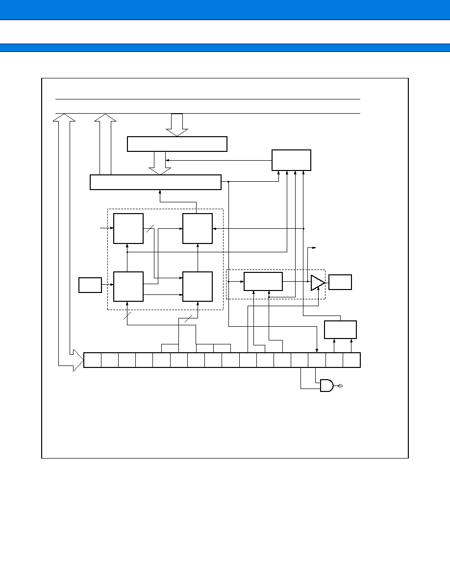
Block Diagram
RESV MCM WS1 WS0 RESV MCS CS1 CS0
STP
Pin
Pin
Pin
SLP
SPL RST TMD CG1
CPU intermittent
operation selecter
Pin high
impedance
control circuit
Internal reset
generation
circuit
CPU clock
control circuit
Peripheral clock
control circuit
CG0 RESV
2
2
X0
X1
RST
RST
Release reset
Cancel interrupt
Clock generator
Low power mode control register (LPMCR)
Pin Hi-z control
Internal reset
CPU clock
Stop and sleep signals
Stop signal
Machine clock
Clock selector
Clock selection register (CKSCR)
Timebase timer
System clock
generation circuit
Oscillation stabilization
wait is passed
Peripheral clock
Oscillation stabilization
wait interval selector
Select intermittent cycles
Standby control
circuit
PLL multipiler
circuit
×
1
×
2
×
3
×
4
Divide-
by-4
Divide-
by-4
Divide-
by-4
Divide-
by-2
Divide-
by-512
Divide-
by-2
Main clock
3
MB90460 Series
32
2.
I/O Ports
(1) Outline of I/O ports
When a data register serving for control output is read, the data output from it as a control output is read regardless
of the value in the direction register. Note that, if a read-modify-write instruction (such as a bit set instruction) is
used to preset output data in the data register when changing its setting from input to output, the data read is
not the data register latched value but the input data from the pin.
Ports 0 to 4 and 6 are input/output ports which serve as inputs when the direction register value is "0" or as
outputs when the value is "1".
Port 5 are input/output ports as other port when ADER is 00
H
.
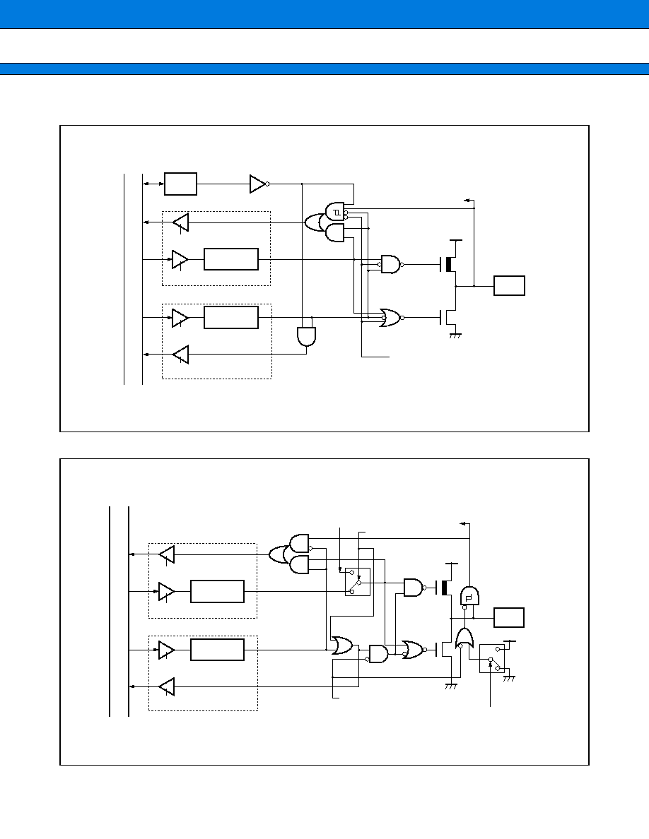
Block Diagram
· Block diagram of Port 0 pins
(Continued)
RDR
Port data register (PDR)
Resource output enable
Pull-up resistor
About 50 K
Standby control (SPL
=
1)
PDR read
PDR write
DDR write
DDR read
Port data direction register (DDR)
Internal data bus
Output latch
Pin
Resource output
Direction
latch
Direct resource input
MB90460 Series
33
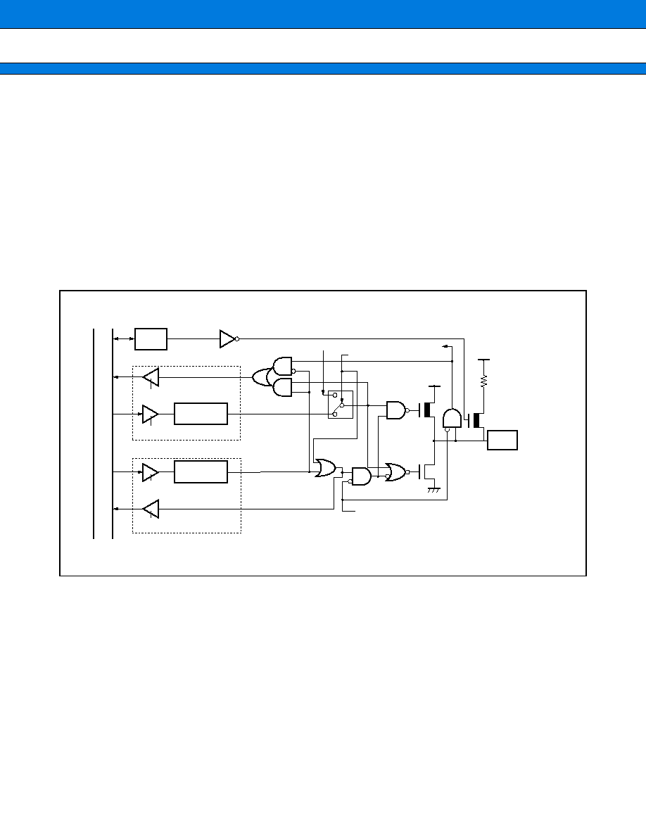
· Block diagram of Port 1 pins
· Block diagram of Port 2 pins
(Continued)
RDR
Port data register (PDR)
Resource output enable
Pull-up resistor
About 50 K
Standby control (SPL
=
1)
PDR read
PDR write
DDR write
DDR read
Port data direction register (DDR)
Internal data bus
Output latch
Pin
Resource output
Direction
latch
Resource input
Port data register (PDR)
Resource output enable
Standby control (SPL
=
1)
PDR read
PDR write
DDR write
DDR read
Port data direction register (DDR)
Internal data bus
Output latch
Pin
Resource output
Direction
latch
Resource input
MB90460 Series
34
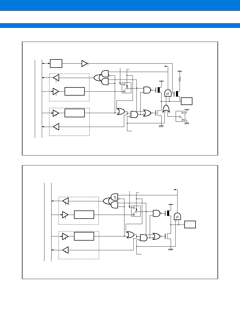
· Block diagram of Port 3 pins
· Block diagram of Port 4 pins
(Continued)
Port data register (PDR)
Resource output enable
Standby control (SPL
=
1)
PDR read
PDR write
DDR write
DDR read
Port data direction register (DDR)
Internal data bus
Output latch
Pin
Resource output
Direction
latch
Port data register (PDR)
Resource output enable
Standby control (SPL
=
1)
PDR read
PDR write
DDR write
DDR read
Port data direction register (DDR)
Internal data bus
Output latch
Pin
Resource output
Direction
latch
Resource input
MB90460 Series
35
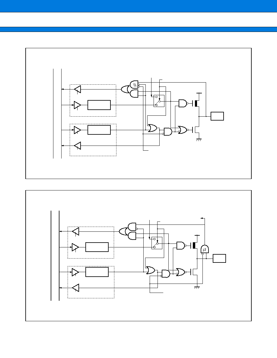
(Continued)
· Block diagram of Port 5 pins
· Block diagram of Port 6 pins
ADER
Port data register (PDR)
Standby control (SPL
=
1)
PDR read
PDR write
DDR write
DDR read
Port data direction register (DDR)
Internal data bus
Output latch
Pin
Direction
latch
Analog input
Port data register (PDR)
Resource output enable
Standby control (SPL
=
1)
PDR read
PDR write
DDR write
DDR read
Port data direction register (DDR)
Internal data bus
Output latch
Pin
Resource output
External interrupt enable
Direction
latch
Resource input
MB90460 Series
36
3.
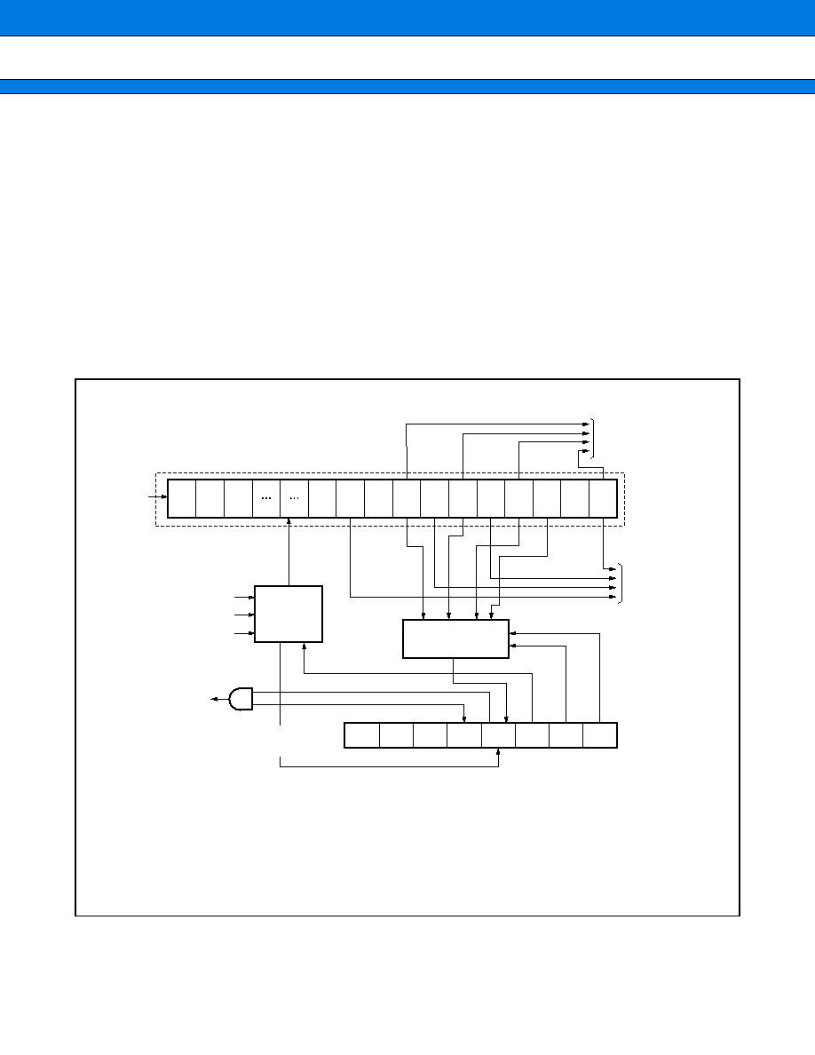
Timebase Timer
The timebase timer is an 18-bit free-running counter (timebase counter) that counts up in synchronization to the
internal count clock (main oscillator clock divided by 2) .
Features of timebase timer :
· Interrupt generated when counter overflow
· EI
2
OS supported
· Interval timer function :
An interrupt generated at four different time intervals
· Clock supply function :
Four different clocks can be selected as a watchdog timer's count clock
Supply clock for oscillation stabilization
Block Diagram
TBIE TBOF TBR TBC1 TBC0
×
2
1
×
2
2
×
2
3
×
2
8
×
2
9
×
2
10
×
2
11
×
2
12
×
2
13
×
2
14
×
2
15
×
2
16
×
2
18
×
2
17
OF
Counter
clear circuit
Interval
timer selector
OF
OF
OF
Timebase
timer counter
Counter clear
Timebase timer
interrupt signal #36
(24
H
)*
2
TBOF clear
TBOF set
To
watchdog
timer
To the oscillation
setting time selector
in the clock control
section
Divide-by
-two HCLK
Power-on reset
Stop mode start
CKSCR : MCS
=
1 to 0 *
1
Timebase timer interrpt
register (TBTC)
OF : Overflow
HCLK : Oscillation clock
*1 : Switching of the machine clock from the oscillation clock to the PLL clock
*2 : Interrupt number
MB90460 Series
37
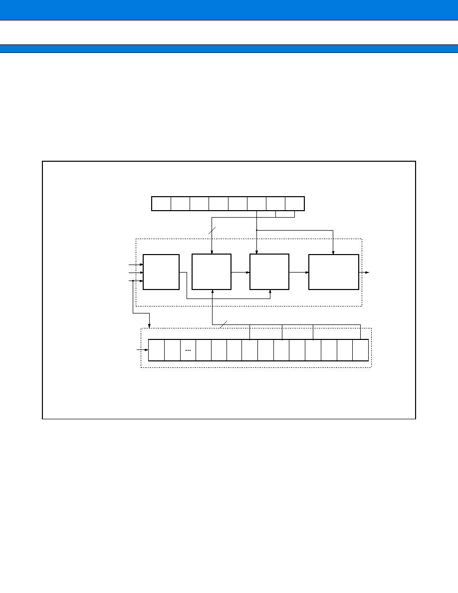
4.
Watchdog Timer
The watchdog timer is a 2-bit counter that uses the timebase timer's supply clock as the count clock. After
activation, if the watchdog timer is not cleared within a given period, the CPU will be reset.
· Features of Watchdog Timer :
Reset CPU at four different time intervals
Status bits to indicate the reset causes
Block Diagram
PONR STBR WRST ERST SRST WTE
WT1
WT0
×
2
1
×
2
2
×
2
8
×
2
9
×
2
10
×
2
11
×
2
12
×
2
13
×
2
14
×
2
15
×
2
16
×
2
17
×
2
18
2
4
Counter
clear control
circuit
Count
clock
selector
2-bit
counter
Watchdog
reset generator
One-half of HCLK
Watchdog timer control register (WDTC)
Watchdog timer
Activation
with CLR
To the
internal
reset
generator
CLR
CLR
Clear
(Timebase timer counter)
Over-
flow
Start of sleep mode
Start of hold status mode
Start of stop mode
HCLK : Oscillation clock

MB90460 Series
38
5.
16 bit reload timer (
×
×
×
×
2)
The 16-bit reload timer provides two operating mode, internal clock mode and event count mode. In each
operating mode, the 16-bit down counter can be reloaded (reload mode) or stopped when underflow (one-shot
mode) .
Output pins TO1 - TO0 are able to output different waveform accroding to the counter operating mode. TO1 -
TO0 toggles when counter underflow if counter is operated as reload mode. TO1 - TO0 output specified level
(H or L) when counter is counting if the counter is in one-shot mode.
Features of the 16 bit reload timer :
· Interrupt generated when timer underflow
· EI
2
OS supported
· Internal clock operating mode :
Three internal count clocks can be selected
Counter can be activated by software or exteranl trigger (singal at TIN1 - TIN0 pin)
Counter can be reloaded or stopped when underflow after activated
· Event count operating mode :
Counter counts down by one when specified edge at TIN1 - TIN0 pin
Counter can be reloaded or stopped when underflow
MB90460 Series
39
Block Diagram
TMRD0*
1
<TMRD1>
Reload signal
Wait signal
Count clock generation
circuit
Machine
clock
TMR0*
1
<TMR1>
P15/TIN0*
1
<P20/TIN1>
CLK
Gate
input
Clear
Internal
clock
Select
signal
EN
CLK
Invert
Output control circuit
To UART0 and
UART1 *
1
<To the A/D
converter>
Interrupt request signal
#30 (1E
H
)*
2
<#32 (20
H
)>
P16/TO0*
1
<P21/TO1>
External clock
Function selection
Timer control status register (TMCSR0)*
1
<TMCSR1>
3
3
2
CSL1 CSL0 MOD2
F
2
MC-16LX Bus
16-bit reload register
16-bit timer register
Prescaler
Input
control
circuit
Pin
Pin
Valid
clock
judgment
circuit
Clock
selector
Output signal
generation
circuit
Operation
control
circuit
Reload
control circuit
MOD1MOD0 OUTE OUTL RELD
UF
INTE
CNTE TRG
*1 : This register includes channel 0 and channel 1. The register enclosed in
<
and
>
indicates the
channel 1 register.
*2 : Interrupt number
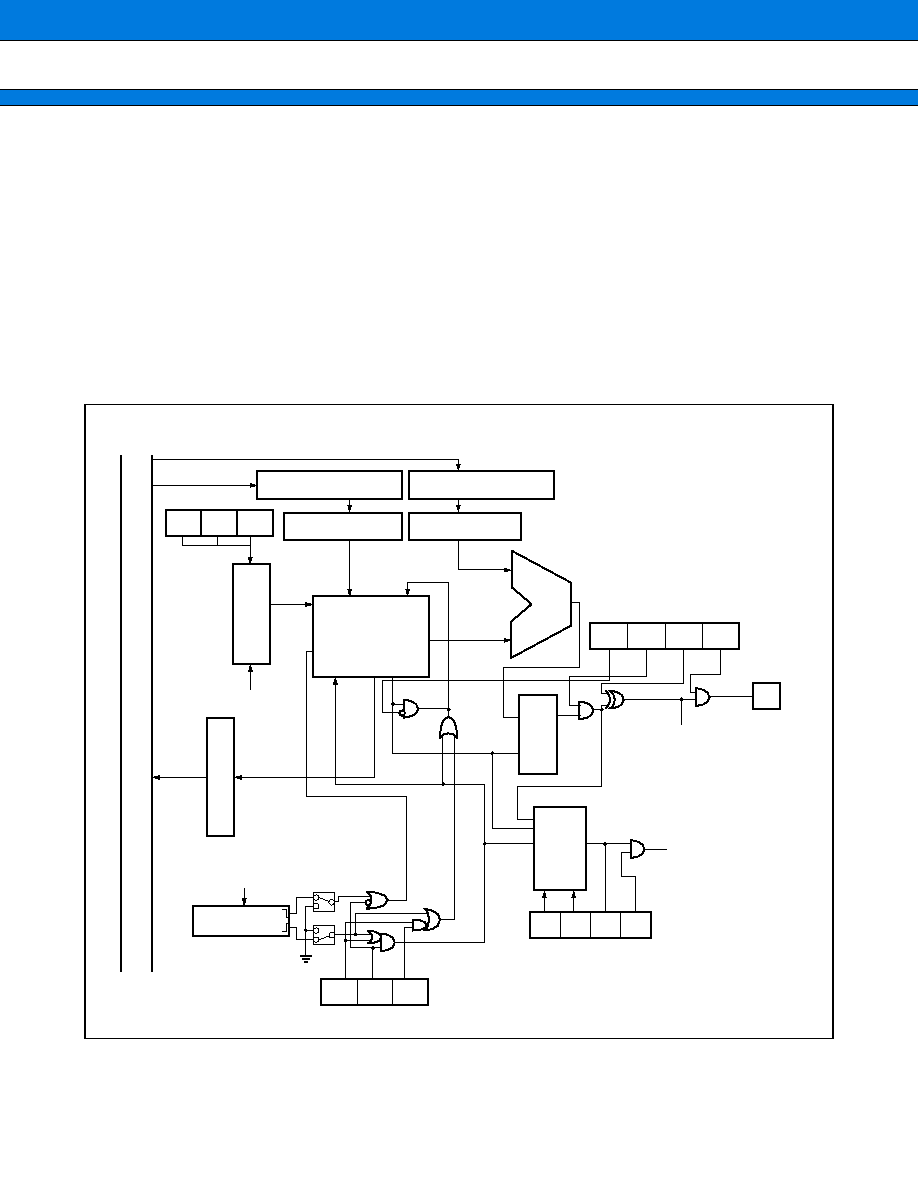
MB90460 Series
40
6.
16-bit PPG Timer (
×
×
×
×
3 )
The 16-bit PPG timer consists of a 16-bit down counter, prescaler, 16-bit period setting buffer register, 16-bit
duty setting buffer register, 16-bit control register and a PPG output pin. This module can be used to output
pulses synchronized by software trigger or GATE signal from Multi-functional timer, refer to "Multi-functional
Timer"
Features of 16-bit PPG Timer :
· Two operating mode : PWM and One-shot
· 8 types of counter operation clock (
,
/2,
/4,
/8,
/16,
/32,
/64,
/128) can be selected
· Interrupt generated when trigger signal arrived, or counter borrow, or change of PPG output
· EI
2
OS supported
Block Diagram
Prescaler
CKS2 CKS1 CKS0
Period Setting
Buffer Register 0/1/2
Duty Setting
Buffer Register 0/1/2
Duty Setting
Register 0/1/2
Period Setting
Register 0/1/2
1/1
1/2
1/4
1/8
1/16
1/32
1/64
1/128
Machine clock
Down Counter
Register 0/1/2
GATE-from multi-functional
timer (for PPG ch. 0 only)
Edge detection
CLK
LOAD
BORROW
START
STOP
16-bit
down counter
Comparator
S
Q
R
MDSE PGMS OSEL POEN
Pin
P37/PPG0
or
P36/PPG1
or
P46/PPG2
PPG0 (multi-functional timer)
or
PPG1 (multi-pulse generator)
or
PPG2
Interrupt
selection
Interrupt
#14/#16/#32
IRS1 IRS0 IRQF IREN
F
2
MC-16LX Bus
(for PPG ch. 1 & 2)
STGR CNTE RTRG

MB90460 Series
41
7.
Multi-functional Timer
The 16-bit multi-functional timer module consists of one 16-bit free-running timer, four input capture circuits, six
output comparators and one channel of 16-bit PPG timer. This module allows six independent waveforms
generated by PPG timer or waveform generator to be outputted. With the 16-bit free-run timer and the input
capture circuit, a input pulse width measurement and external clock cycle measurement can be done.
(1) 16-bit free-running timer (1 channel)
· The 16-bit free-running timer consists of a 16-bit up/up-down counter, control register, 16-bit compare clear
register (with buffer register) and a prescaler.
· 8 types of counter operation clock (
,
/2,
/4,
/8,
/16,
/32,
/64,
/128) can be selected. (
is the machine
clock)
· Two types of interrupt causes :
- Compare clear interrupt is generated when there is a comparing match with compare clear register and 16-
bit free-run timer.
- Zero detection interrupt is generated while 16-bit free-running timer is detected as zero in count value.
· EI
2
OS supported
· The compare clear register has a selectable buffer register, into which data is written for transfer to the compare
clear register. When the timer is stopped, transfer occurs immediately when the data is written to the buffer.
When the timer is operation, data transfer from the buffer occurs when the timer value is detected to be zero.
· Reset, software clear, compare match with compare clear register in up-count mode will reset the counter
value to "0000
H
".
· Supply clock to output compare module :
The prescaler ouptut is acted as the count clock of the output compare.
(2) Output compare module (6 channels)
· The output compare module consists of six 16-bit compare registers (with selectable buffer register) , compare
output latch and compare control registers. An interrupt is generated and output level is inverted when the
value of 16-bit free-running timer and compare register are matched.
· 6 compare registers can be operated independently.
· Output pins and interrupt flag are corresponding to each compare register.
· Inverts output pins by using 2 compare registers together. 2 compare registers can be paired to control the
output pins.
· Setting the initial value for each output pin is possible.
· Interrupt generated when there is a comparing match with output compare register and 16 bit free-run timer
· EI
2
OS supported
(3) Input capture module (4 channels)
Input capture consists of 4 independent external input pins, the corresponding capture register and capture
control register. By detecting any edge of the input signal from the external pin, the value of the 16-bit free-
running timer can be stored in the capture register and an interrupt is generated simultaneously.
· Operation synchronized with the 16-bit free-run timer's count clock.
· 3 types of trigger edge (rising edge, falling edge and both edge) of the external input signal can be selected
and there is indication bit to show the trigger edge is rising or falling.
· 4 input captures can be operated independently.
· Two independent interrupts are generated when detecting a valid edge from external input.
· EI
2
OS supported
(4) 16-bit PPG timer (
×
×
×
×
1)
The 16-bit PPG timer 0 is used to provide a PPG signal for waveform generator.
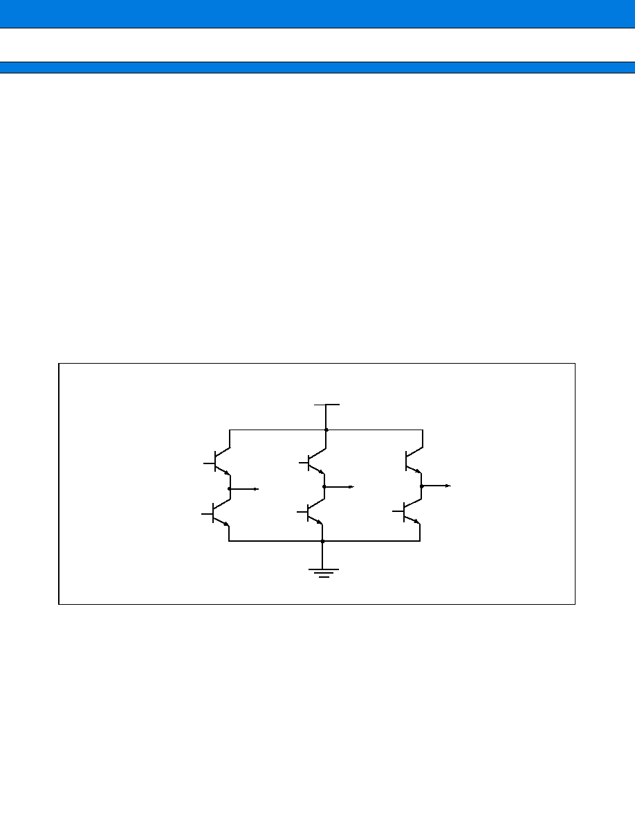
MB90460 Series
42
(5) Waveform Generator module
The waveform generator consists of three 16-bit timer registers, three timer control registers and 16-bit waveform
control register.
With waveform generator, it is possible to generate real time output, 16-bit PPG waveform output, non-overlap
3-phase waveform output for inverter control and DC chopper waveform output.
· It is possible to generate a non-overlap waveform output based on dead-time of 16-bit timer. (Dead-time timer
function)
· It is possible to generate a non-overlap waveform output when realtime output is operated in 2-channel mode.
(Dead-time timer function)
· By detecting realtime output compare match, GATE signal of the PPG timer operation will be generated to
start or stop PPG timer operation. (GATE function)
· When a match is detected by realtime output compare, the 16-bit timer is activated. The PPG timer can be
started or stopped easily by generating a GATE signal for PPG operation until the 16-bit timer stops. (GATE
function)
· Forced to stop output waveform using DTTI0 pin input
· Interrupt generated when DTTI0 active or 16-bit tmer underflow
· EI
2
OS supported
· MCU to 3-phase Motor Interface Circuit
RTO0 (U) , RTO2 (V) , RTO4 (W) are called "UPPER ARM".
RTO1 (X) , RTO3 (Y) , RTO5 (Z) are called "LOWER ARM".
RTO0 (U) and RTO1 (X) are called "non-overlapping output pair".
RTO2 (V) and RTO3 (Y) are called "non-overlapping output pair".
RTO4 (W) and RTO5 (Z) are called "non-overlapping output pair".
(U) , (V) , (W) are the 3-phase coil connection.
RTO4(W)
(V)
RTO5(Z)
(W)
RTO2(V)
(U)
RTO3(Y)
RTO0(U)
RTO1(X)
V
CC
MB90460 Series
43
· 3-phase Motor Coil Connection Circuit
(U)
(V)
(W)
(V)
(W)
(U)
Star Connection Circuit
Delta Connection Circuit
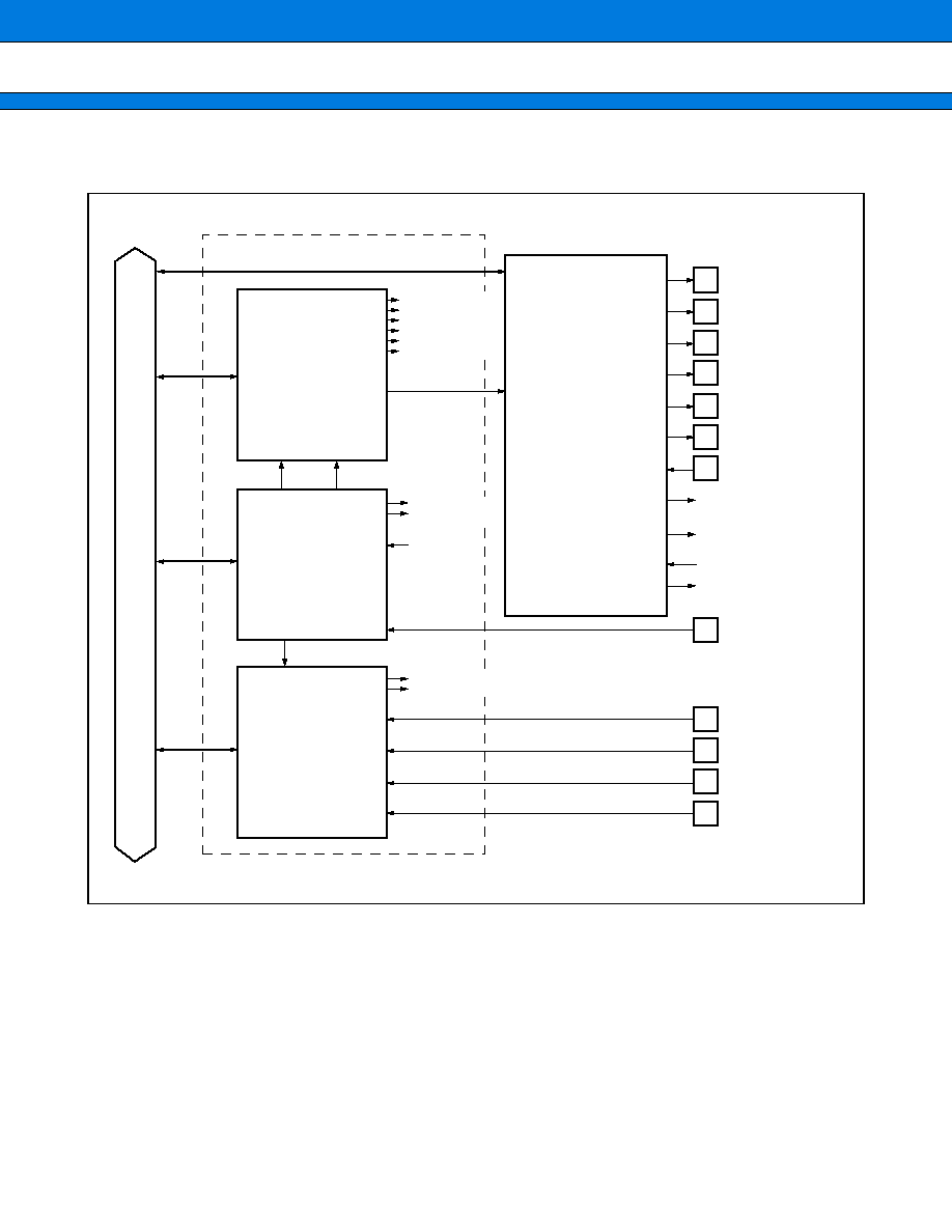
MB90460 Series
44
Block Diagram
· Block Diagram of Multi-functional Timer
(Continued)
Real time I/O
Interrupt#12
Interrupt#15
Interrupt#17
Interrupt#19
Interrupt#21
Interrupt#23
output compare 0
output compare 1
output compare 2
output compare 3
output compare 4
output compare 5
RT0 to 5
16-bit Output
Compare
buffer
transfer
counter
value
16-bit free-
running
timer
Interrupt#31
Interrupt#34
A/D trigger
A/D trigger
EXCK
Zero detect
Compare clear
Input capture 0/1
Input capture 2/3
counter
value
Interrupt #33
Interrupt #35
16-bit Input
Capture
IN0
IN1
IN2
IN3
RT0 to 5
Waveform
generator
RTO0
RTO1
RTO2
RTO3
RTO4
RTO5
DTTI
PPG0
PPG0
GATE
GATE
Interrupt#29
16-bit timer 0/1/2
underflow
Interrupt#20
DTTI0 falling edge detect
Pin
Pin
Pin
Pin
Pin
Pin
Pin
Pin
Pin
Pin
Pin
Pin
P24/IN0
P17/FRCK
P10/INT0/DTTI0
P35/RTO5 (Z)
P34/RTO4 (W)
P33/RTO3 (Y)
P32/RTO2 (V)
P31/RTO1 (X)
P30/RTO0 (U)
P25/IN1
P26/IN2
P27/IN3
F
2
MC-16LX Bus
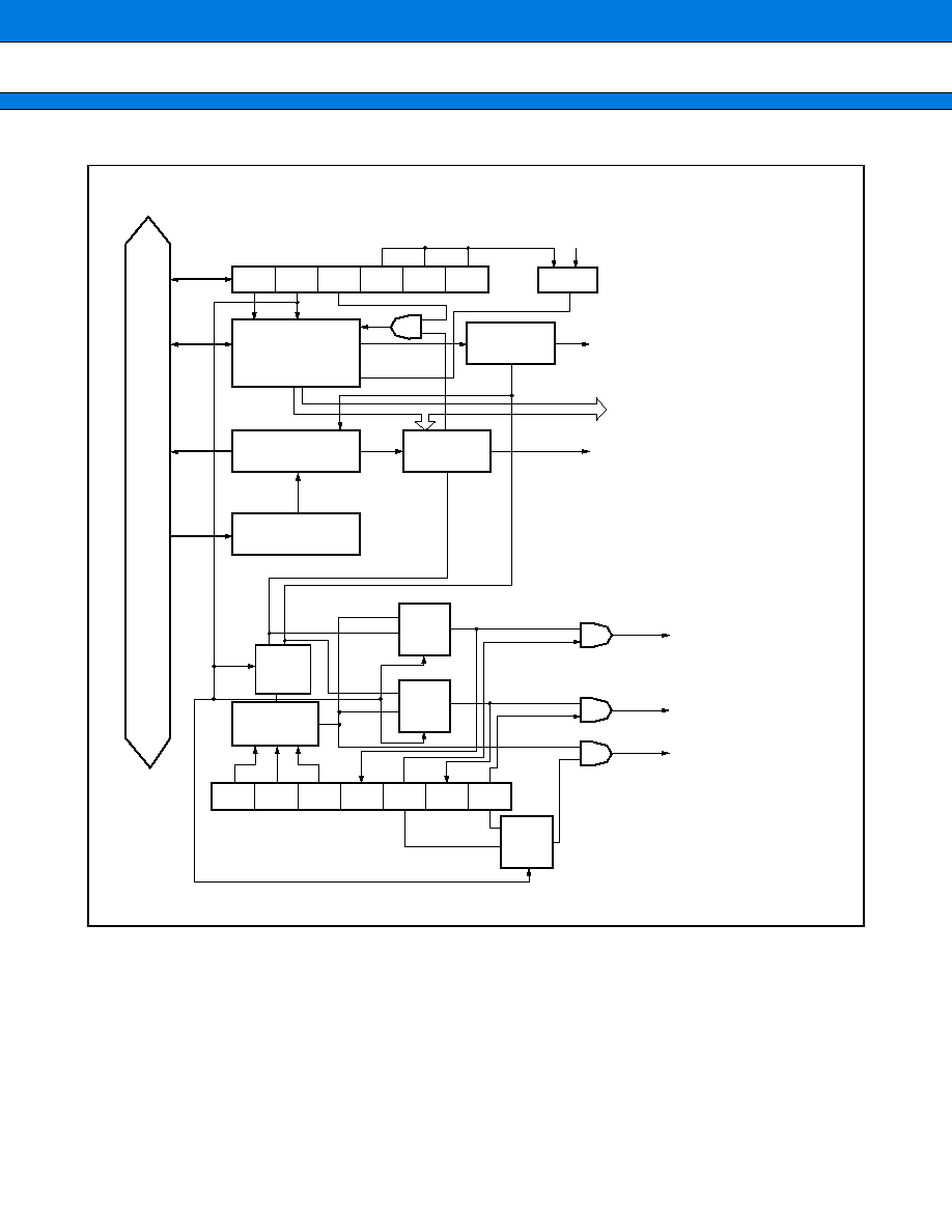
MB90460 Series
45
· Block diagram of 16-bit free-running timer
(Continued)
F
2
MC-16LX BUS
Prescaler
STOP MODE SCLR CLK2 CLK1 CLK0
Zero detect
circuit
Zero detect (to output compare)
STOP
UP/
UP-DOWN
CLR
16-bit free-running
timer
CK
transfer
16-bit compare
clear register
Compare
circuit
To Input Capture &
Output Compare
Compare clear match (to output compare)
16-bit compare
clear buffer register
Selector
I0
I1
O
Mask Circuit
Selector
Selector
I0
I1
I0
I1
O
O
Selector
I0
I1
O
MSI2
MSI1
MSI0
ICLR
ICRE IRQZF IRQZE
A/D trigger
Interrupt #34 (22
H
)
Interrupt #31 (1F
H
)
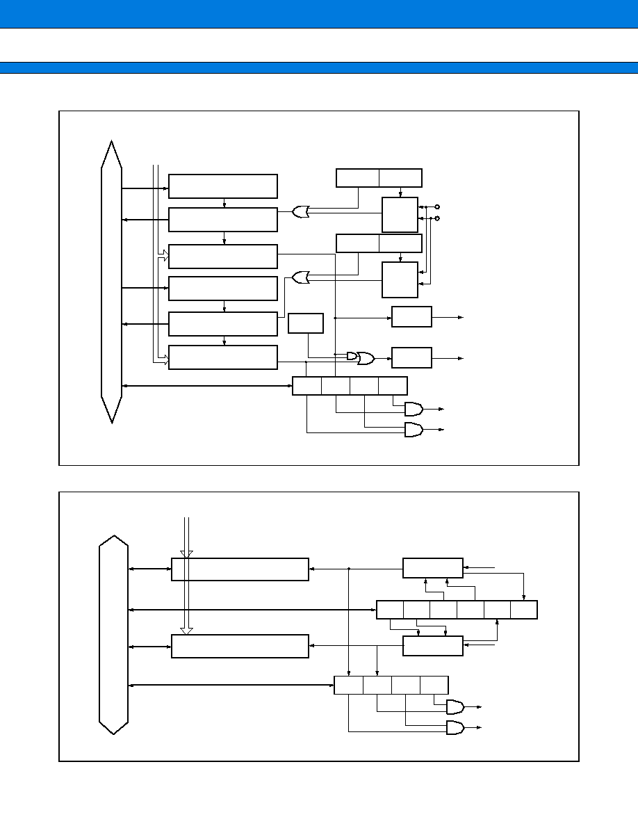
MB90460 Series
46
· Block diagram of 16-bit output compare
· Block diagram of 16-bit input capture
(Continued)
BUF0
BUF1
BTS0
BTS1
Selector
Selector
O
O
I0
I1
I0
I1
Zero detect from
free-running timer
Compare clear match from
free-running timer
Count value from Free-running timer
Compare buffer
register 0/2/4
Compare register 0/2/4
Compare register 1/3/5
Compare circuit
Compare circuit
Compare buffer
register 1/3/5
transfer
transfer
CMOD
F
2
MC-16LX BUS
T
Q
T
Q
RT0/2/4
(Waveform
generator)
RT1/3/5
(Waveform
generator)
IOP1
IOP0
IOE1
IOE0
Interrupt
#12, #17, #21
#15, #19, #23
Count value from Free-running timer
Capture register 0/2
Capture register 1/3
F
2
MC-16LX BUS
Interrupt
#33, #35
#33, #35
IN0/2
IN1/3
Edge detect
Edge detect
EG11 EG10 EG01 EG00
IEI1
IEI0
ICP0
ICP1
ICE0
ICE1
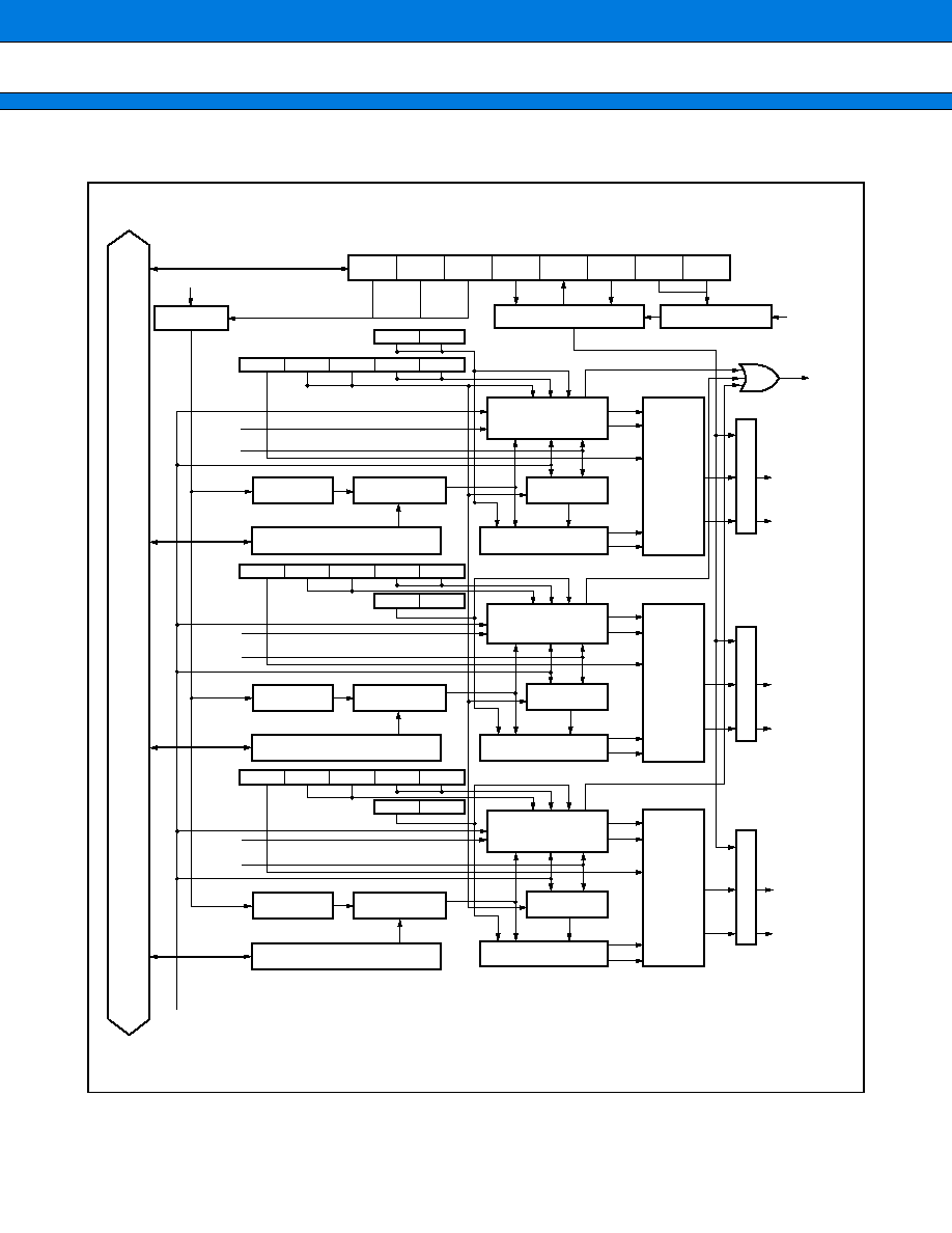
MB90460 Series
47
(Continued)
· Block diagram of waveform generator
F
2
MC-16LX BUS
Divider
DCK2
DCK1
DCK0
NRSL
DTIF
DTIE
NWS1
NWS0
SIGCR
DTTI0
Noise Cancellation
DTTI0 control circuit
GATE 0/1
GATE
(to PPG0)
TO0
TO1
TO2
TO3
TO4
TO5
U
X
V
Y
W
Z
Waveform control
Selector
Output Control
Output Control
Output Control
RTO0 (U)
RTO1 (X)
RTO2 (V)
RTO3 (Y)
RTO4 (W)
RTO5 (Z)
Selector
Selector
Selector
GATE 4/5
GATE 2/3
Dead time generator
Dead time generator
Dead time generator
Selector
Selector
Waveform control
Waveform control
PICSH01
DTCR0
RT0
RT1
RT2
RT3
RT4
RT5
16-bit timer 0
16-bit timer register 0
16-bit timer register 1
16-bit timer register 2
Compare circuit
16-bit timer 1
Compare circuit
16-bit timer 2
Compare circuit
DTCR1
DTCR2
PICSH01
PICSH01
PPG0
TMD2
TMD1 TMD0 GTEN1 GTEN0
TMD2 TMD1 TMD0 GTEN1 GTEN0
TMD2 TMD1 TMD0 GTEN1 GTEN0
PGEN5 PGEN4
PGEN3 PGEN2
PGEN1 PGEN0

MB90460 Series
48
8.
Multi-Pulse Generator
The Multi-pulse Generator consists of a 16-bit PPG timer, a 16-bit reload timer and a waveform sequencer. By
using the waveform sequencer, 16-bit PPG timer output signal can be directed to Multi-pulse Generator output
(OPT5 to 0) according to the input signal of Multi-pulse Generator (SNI2 to 0) . Meanwhile, the OPT5 to 0 output
signal can be hardware terminated by DTTI input (DTTI1) in case of emergency. The OPT5 to 0 output signals
are synchronized with the PPG signal in order to eliminate the unwanted glitch.
The Multi-pulse generator has the following features :
· Output Signal Control
- 12 output data buffer registers are provided
- Output data register can be updated by any one of output data buffer registers when :
1. an effective edge detected at SNI2 - SNI0 pin
2. 16-bit reload timer underflow
3. output data buffer register OPDBR0 is written
· Output data register (OPDR) determines which OPT terminals (OPT5 - 0) output the 16-bit PPG waveform
- Waveform sequencer is provided with a 16-bit timer to measure the speed of motor
- The 16-bit timer can be used to disable the OPT output when the position detection is missing
· Input Position Detect Control
- SNI2 - SNI0 input can be used to detect the rotor position
- A controllable noise filter is provided to the SNI2 - SNI0 input
· PPG Synchronization for Output signal
- OPT output is able to synchronize the edge of PPG waveform to avoid a short pulse (or glitch) appearance
· Vaious interrupt generation causes
· EI
2
OS supported
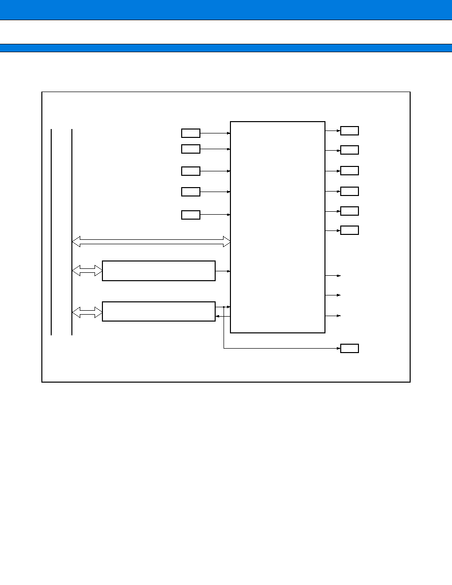
MB90460 Series
49
Block Diagram
· Block diagram of Multi-pulse generator
(Continued)
F
2
MC-16LX Bus
16-BIT PPG TIMER 1
16-BIT RELOAD TIMER 0
TOUT
TIN
PPG1
DTTI
SNI2
SNI1
SNI0
TIN0
Pin
Pin
Pin
Pin
Pin
P12/INT2/DTTI1
P15/INT5/TIN0
P45/SNI2
P44/SNI1
P43/SNI0
PPG1
WIN0
TIN0O
WAVEFORM
SEQUENCER
OPT5
OPT4
OPT3
OPT2
OPT1
OPT0
Pin
Pin
Pin
Pin
Pin
Pin
Pin
P05/OPT5
P04/OPT4
P03/OPT3
P02/OPT2
P01/OPT1
P00/OPT0
P16/INT6/TO0
INTERRUPT #22
INTERRUPT #26
INTERRUPT #28
Interrupt #22
Interrupt #26
Interrupt #28
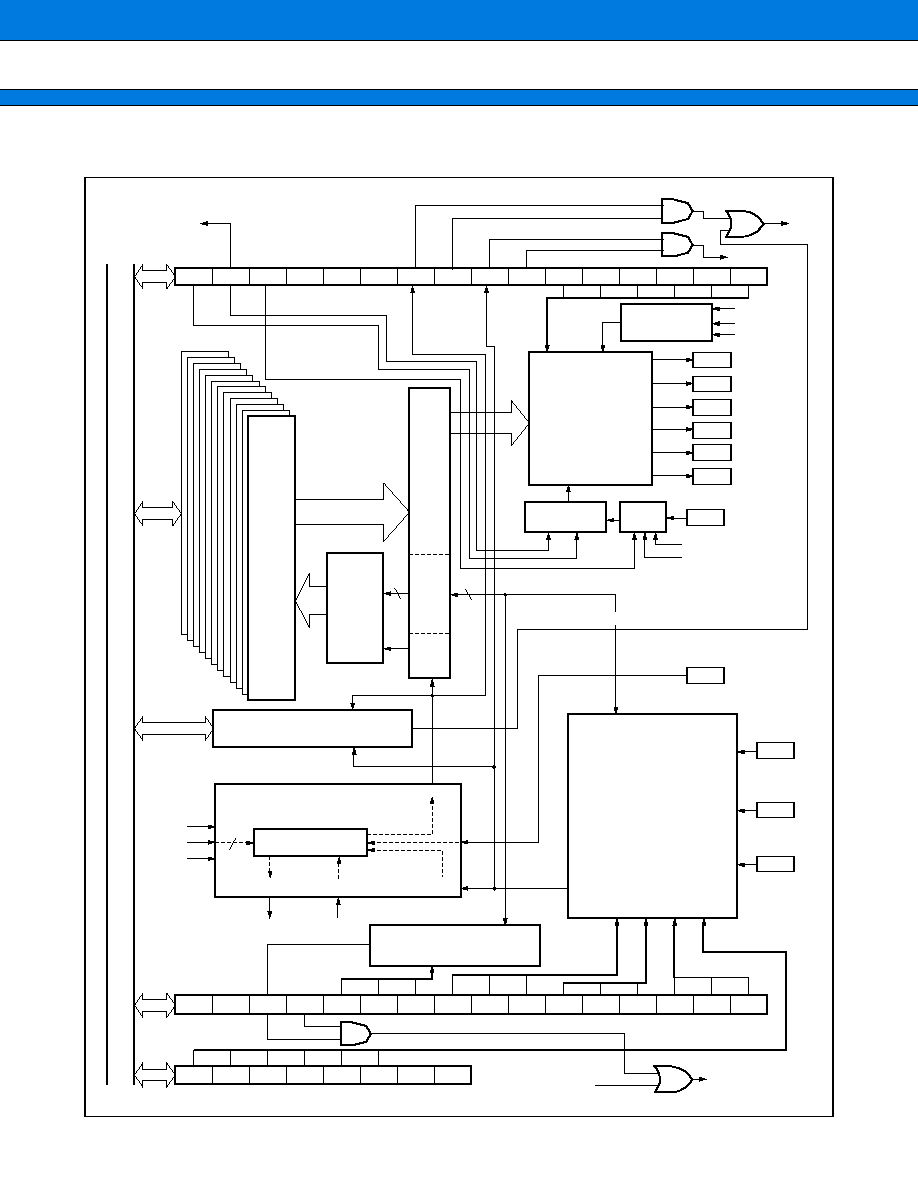
MB90460 Series
50
(Continued)
· Block diagram of waveform sequencer
Interrupt #22
WRITE TIMING INTERRUPT
OPCR Register
POSITION DETECTION INTERRUPT
Interrupt
#26
PDIRT
From PPG1
WTS1
WTS0
SYN Circuit
Pin
Pin
Pin
Pin
Pin
Pin
P00/OPT0
P01/OPT1
P02/OPT2
P03/OPT3
P04/OPT4
P05/OPT5
P12/INT2/DTTI1
Pin
D1
D0
Noise
Filter
DTTI1 Control
Circuit
OUTPUT
CONTROL
CIRCUIT
DTIE DTIF NRSL OPS2 OPS1 OPS0 WTIF WTIE PDIF PDIE OPE5 OPE4 OPE3 OPE2 OPE1 OPE0
OPDBRB to 0 Registers
OUTPUT DATA BUFFER REGISTER
×
12
DECODER
OPDR Register
OP
×
1/OP
×
0
RDA2 to 0
BNKF
3
3
COMPARE CLEAR INTERRUPT
F
2
MC-16LX Bus
16-BIT TIMER
WTO
WTIN1
CCIRT
Pin
P15/INT5/TIN0
P43/SNI0
P44/SNI1
P45/SNI2
Pin
Pin
Pin
POSITION
DETECT
CIRCUIT
WTIN1
WTIN1
3
OPS2
OPS1
OPS0
TIN0O
DATA WRITE
CONTROL UNIT
SELECTOR
TIN0O
WTIN0
WTIN0
WTO
COMPARISON CIRCUIT
IPCR Register
NCCR Register
WTS1 WTS0 CPIF CPIE CPD2 CPD1 CPD0 CMPE CPE1 CPE0 SNC2 SNC1 SNC0 SEE2 SEE1 SEE0
PDIRT
Interrupt #28
COMPARE MATCH INTERRUPT
D0
D1
S00
S01
S10
S11
S20
S21

MB90460 Series
51
9.
PWC Timer
The PWC (pulse width count) timer is a 16-bit multi-function up-counter with reload timer functions and input-
signal pulse-width count functions as well.
The PWC timer consists of a 16-bit counter, on input pulse divider, a divide ratio control register, a count input
pin, a pulse output pin, and a 16-bit control register.
The PWC timer has the following features :
· Interrupt generated when timer overflow or end of PWC measurement.
· EI
2
OS supported
· Timer functions :
- Generates an interrupt request at set time intervals.
- Outputs pulse signals synchronized with the timer cycle.
- Selects the counter clock from among three internal clocks.
· Pulse-width count functions
- Counts the time between external pulse input events.
- Selects the counter clock from among three internal clocks.
- Count mode
·
H pulse width (rising edge to falling edge) /L pulse width (falling edge to rising edge)
·
Rising-edge cycle (rising edge to falling edge) /Falling-edge cycle (falling edge to rising edge)
·
Count between edges (rising or falling edge to falling or rising edge)
Capable of counting cycles by dividing input pulses by 2
2
, 2
4
, 2
6
, 2
8
using an 8-bit input divider.
Generates an interrupt request upon the completion of count operation.
Selects single or consecutive count operation.
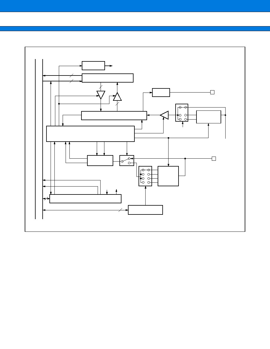
MB90460 Series
52
Block Diagram
ERR
PWC read
PWC
Reload
Overflow
Data transfer
16
16
16
Error
detection
16
16-bit up count timer
Control circuit
Clock
F.F.
Clock
divider
Edge
detection
F
2
MC-16LX b
u
s
Wr
ite enab
led
15
ERR
CKS0
CKS1
PWCS
DIVR
8-bit
divider
2
2
2
2
3
P06/PWI0
P22/PWI1
P07/PWO0
P23/PWO1
Division
rate
selection
Start edge
selection
Count end
edge
End edge
selection
Count bit
output
Flag setting
Divider ON/OFF
Overflow
Timer clear
Count
enabled
Count start edge
Count end interrupt request
Overflow interrupt request
CKS1, CKS0,
Divider clear
Internal clock
(machine clock / 4)

MB90460 Series
53
10. UART
The UART is a serial I/O port for asynchronous (start-stop) communication or clock-synchronous communication.
The UART has the following features :
· Full-duplex double buffering
· Capable of asynchronous (start-stop bit) and CLK-synchronous communications
· Support for the multiprocessor mode
· Various method of baud rate generation :
- External clock input possible
- Internal clock (a clock supplied from 16-bit reload timer can be used.)
- Embedded dedicated baud rate generator
* : Assuming internal machine clock frequencies of 6, 8, 10, 12, and 16 MHz
· Error detection functions (parity, framing, overrun)
· NRZ (Non Return to Zero) Signal format
· Interrupt request :
- Receive interrupt (receive complete, receive error detection)
- Transmit interrupt (transmission complete)
- Transmit / receive conforms to extended intelligent I/O service (EI
2
OS)
· Flexible data length :
- 7 bit to 9 bit selective (without a parity bit)
- 6 bit to 8 bit selective (with a parity bit)
Operation
Baud rate
Asynchronous
31250/9615/4808/2404/1202 bps
CLK synchronous
2 M/1 M/500 K/250 K/125 K/62.5 Kbps
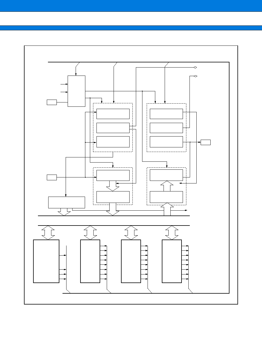
MB90460 Series
54
Block Diagram
PE
ORE
FRE
RDRF
TDRE
BDS
RIE
TIE
MD1
MD0
CS2
CS1
CS0
RST
SCKE
SOE
PEN
P
SBL
CL
A/D
REC
RXE
TXE
MD
DIV2
DIV1
DIV0
SOT0, 1
SCK0, 1
SIN0, 1
Clock
selector
Reception
control
circuit
Reception clock
Reception bit
counter
Reception parity
counter
Start bit
detection circuit
Send clock
send control
circuit
Send start circuit
Send bit counter
Send parity counter
Reception interrupt
request output
Send interrupt
request output
End of reception
Start of transmission
Reception
shift register
Send shift register
Reception status
determination circuit
16-bit reload timer
Dedicated baud
rate generator
Control bus
Pin
Pin
Pin
Serial input
data register (0, 1)
Serial output
data register (0, 1)
receive error
generation signal
(to CPU)
2
EI OS
Internal data bus
Serial
status
register
0, 1
Serial
control
register
0, 1
Serial
mode
register
0, 1
Communication
prescaler
control
register
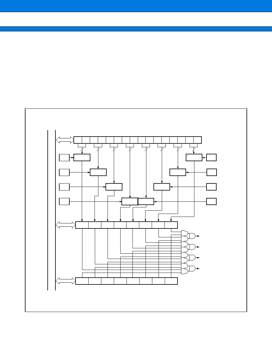
MB90460 Series
55
11. DTP/External Interrupts
The DTP/external interrupt circuit is activated by the signal supplied to a DTP/external interrupt pin. The CPU
accepts the signal using the same procedure it uses for normal hardware interrupts and generates external
interrupts or activates the extended intelligent I/O service (EI
2
OS) .
Features of DTP/External Interrupt :
· Total 8 external interrupt channels
· Two request levels ("H" and "L") are provided for the intelligent I/O service.
· Four request levels (rising edge, falling edge, "H" level and "L" level) are provided for external interrupt requests.
Block Diagram
LB7
ER7
ER6
ER5
ER4
ER3
ER2
ER1
ER0
EN7
EN6
EN5
EN4
EN3
EN2
EN1
EN0
P63/INT7
P10/INT0/DTTI0
LA7 LB6 LA6 LB5 LA5 LB4 LA4 LB3 LA3 LB2 LA2 LB1 LA1 LB0 LA0
P16/INT6/TO0
P11/INT1
P12/INT2/DTTI1
P13/INT3
P15/INT5/TIN0
P14/INT4
Pin
Pin
Pin
Pin
Pin
Pin
Selector
Selector
Selector
Selector
Pin
Pin
Internal data bus
Selector
Selector
Selector
Selector
#20(14
H
)
Interrupt request number
Request level setting register (ELVR)
#22(16
H
)
#25(19
H
)
#27(1B
H
)
2
2
2
2
2
2
2
2
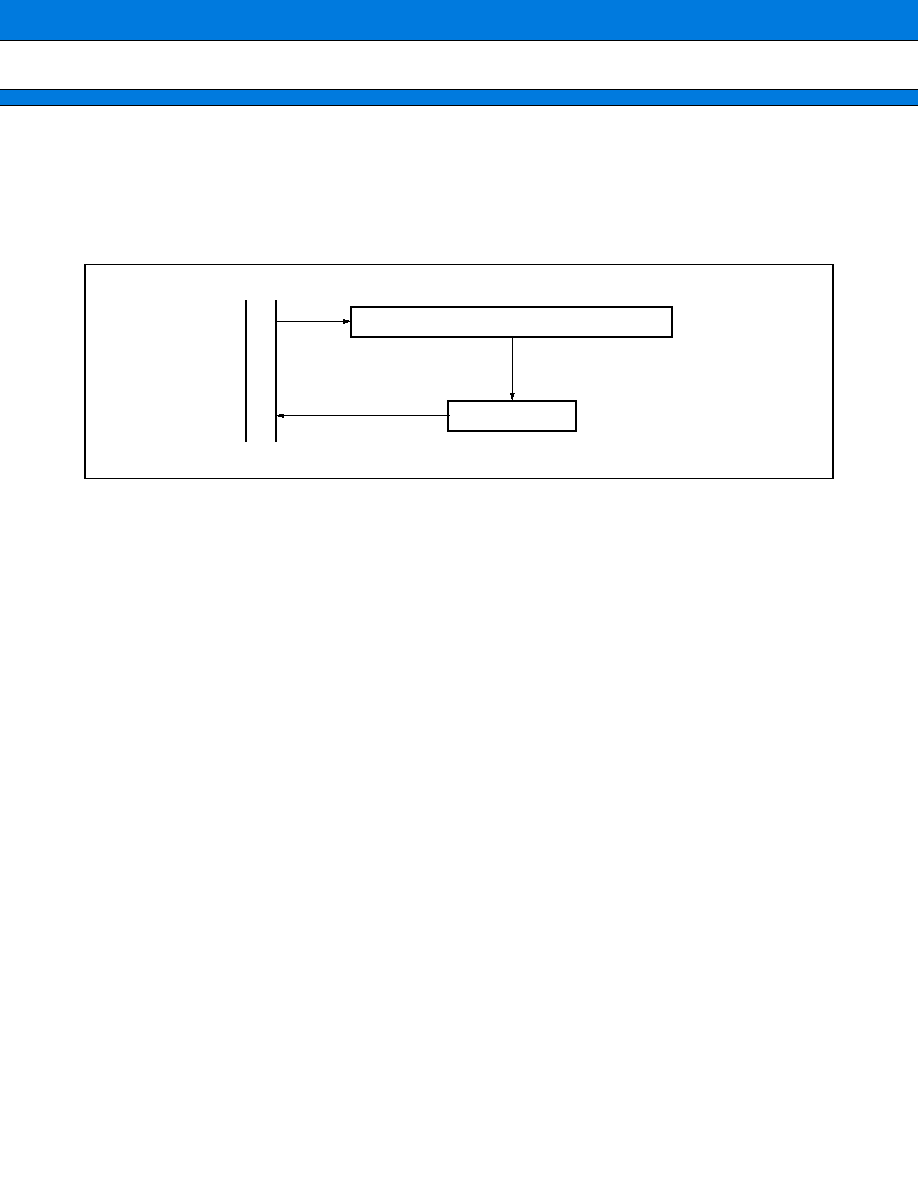
MB90460 Series
56
12. Delayed Interrupt Generation Module
The delayed interrupt generation module is used to generate a task switching interrupt. Interrupt requests to the
F
2
MC-16LX CPU can be generated and cleared by software using this module.
Block Diagram
Delayed interrupt cause issuance/cancellation decoder
Interrupt cause latch
F
2
MC- 16LX bus

MB90460 Series
57
13. A/D Converter
The converter converts the analog voltage input to an analog input pin (input voltage) to a digital value. The
converter has the following features :
· The minimum conversion time is 6.13
µ
s (for a machine clock of 16 MHz; includes the sampling time) .
· The minimum sampling time is 2.0
µ
s (for a machine clock of 16 MHz) .
· The converter uses the RC-type successive approximation conversion method with a sample hold circuit.
· A resolution of 10 bits or 8 bits can be selected.
· Up to eight channels for analog input pins can be selected by a program.
· Various conversion mode :
- Single conversion mode : Selectively convert one channel.
- Scan conversion mode : Continuously convert multiple channels. Maximum of 8 program selectable channels.
- Continuous conversion mode : Repeatedly convert specified channels.
- Stop conversion mode : Convert one channel then halt until the next activation. (Enables synchronization of
the conversion start timing.)
· At the end of A/D conversion, an interrupt request can be generated and EI
2
OS can be activated.
· In the interrupt-enabled state, the conversion data protection function prevents any part of the data from being
lost through continuous conversion.
· The conversion can be activated by software, 16-bit reload timer 1 (rising edge) and 16-bit free-running timer
zero detection edge.
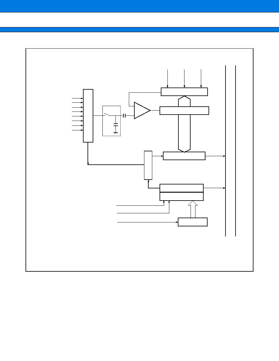
MB90460 Series
58
Block Diagram
MPX
AV
SS
AVR
D/A converter
AV
CC
AN0
AN1
AN2
AN3
AN4
AN5
AN6
AN7
ADCS0/1
ADCR0/1
16-bit reload timer 1
16-bit free-running timer zero detection
Sequential compare register
Data register
Comparator
Input circuit
Sample and hold circuit
Prescaler
A/D control register 0
A/D control register 1
Operation clock
F
2
MC-16LX bus
Decoder
: Machine clock
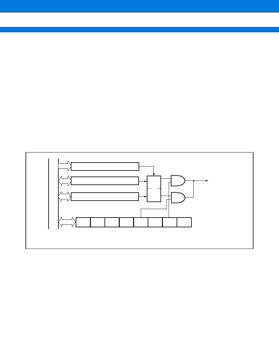
MB90460 Series
59
14. ROM Correction Function
In the case that the address of the instruction after the one that a program is currently processing matches the
address configured in the detection address configuration register, the program forces the next instruction to be
processed into an INT9 instruction, and branches to the interrupt process program. Since processing can be
conducted using INT9 interrupts, programs can be repaired using batch processing.
·
·
·
·
Overview of the Rom correction Function
· The address of the instruction after the one that a program is currently processing is always stored in an
address latch via the internal data bus. Address match detection constantly compares the address stored in
the address latch with the one configured in the detection address configuration register. If the two compared
addresses match, the CPU forcibly changes this instruction into an INT9 instruction, and executes an interrupt
processing program.
· There are two detection address configuration registers : PADR0 and PADR1. Each register provides an
interrupt enable bit. This allows you to individually configure each register to enable/prohibit the generation of
interrupts when the address stored in the address latch matches the one configured in the detection address
configuration register.
Block Diagram
· Address latch
Stores value of address output to internal data bus.
· Address detection control register (PACSR)
Set this register to enable/prohibit interrupt output when an address match is detected.
· Detection address configuration register (PADR0, PADR1)
Configure an address with which to compare the address latch value.
PACSR
PADR0 (24 bit)
PADR1 (24 bit)
Address latch
Detection address configuration register 0
Detection address configuration register 1
Comparator
INT9 instruction
(INT9 interrupt generation)
Re-
served
Re-
served
Re-
served
AD0E
Re-
served
AD1E
Re-
served
Re-
served
Internal data bus
Address detection control register (PACSR)
Reseved : Make sure this is always set to "01"
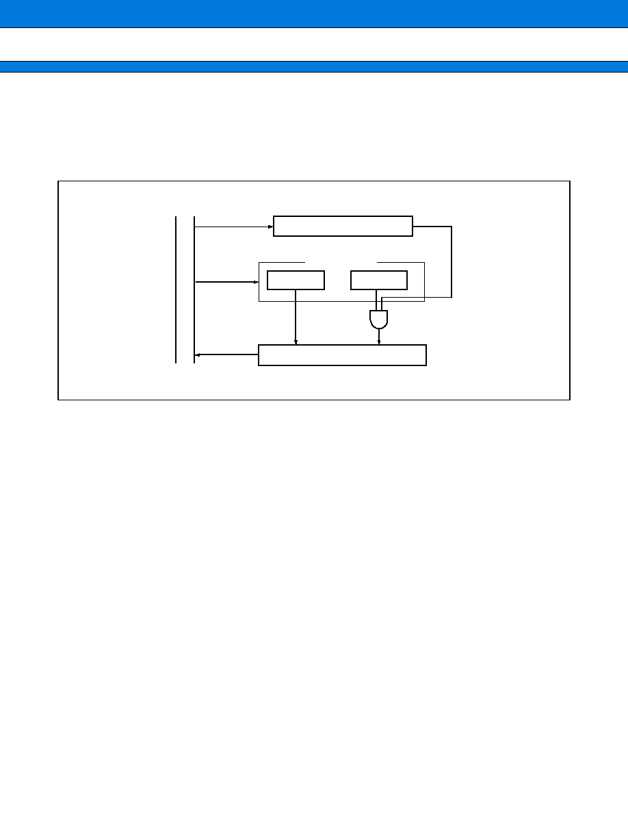
MB90460 Series
60
15. ROM Mirroring Function Selection Module
The ROM mirroring function selection module can select what the FF bank allocated the ROM and see through
the 00 bank according to register settings.
Block Diagram
ROM
ROM mirroring register
Address area
FF bank
00 bank
F
2
MC-16LX bus
MB90460 Series
61
16. 512 Kbit Flash Memory
The 512 Kbit flash memory is allocated in the FE
H
to FF
H
banks on the CPU memory map. Like masked ROM,
flash memory is read-accessible and program-accessible to the CPU using the flash memory interface circuit.
The flash memory can be programmed/erased by the instruction from the CPU via the flash memory interface
circuit. The flash memory can therefore be reprogrammed (updated) while still on the circuit board under inte-
grated CPU control, allowing program code and data to be improved efficiently.
Note that sector operations such as "enable sector protect" cannot be used.
Features of 512 Kbit flash memory
· 64 kwords
×
8 bits/32 kwords
×
16 bits (16 k
+
8 k
+
8 k
+
32 k) sector configuration
· Automatic program algorithm (same as the Embedded Algorithm* : MBM29F400TA)
· Installation of the deletion temporary stop/delete restart function
· Write/delete completion detected by the data polling or toggle bit
· Write/delete completion detected by the CPU interrupt
· Compatibility with the JEDEC standard-type command
· Each sector deletion can be executed (Sectors can be freely combined) .
· Flash security feature
· Number of write/delete operations 10,000 times guaranteed.
· Flash reading cycle time (Min) 2 machine cycles
* : Embedded Algorithm is a trademark of Advanced Micro Devices, Inc.
(1) Register configuration
Flash Memory Control status register
Bit number
Address : 0000AE
H
FMCS
Read/write
Initial value
R/W
0
R/W
0
R
1
W
0
W
0
W
0
R/W
0
7
6
5
4
3
2
1
0
RDYINT
R/W
0
INTE
WE
RDY
Reserved
LPM1
Reserved
LMP0

MB90460 Series
62
(2) Sector configuration of 512Kbit flash memory
The 512 Kbit flash memory has the sector configuration illustrated below. The addresses in the illustration are
the upper and lower addresses of each sector.
When accessed from the CPU, SA0 to SA3 are allocated in the FF bank registers, respectively.
* : Programmer addresses correspond to CPU addresses when data is programmed in flash memory by a parallel
programmer. Programmer addresses are used to program/erase data using a general-purpose programmer.
FFFFFF
H
FFC000
H
FFBFFF
H
FFA000
H
FF9FFF
H
FF8000
H
FF7FFF
H
FF0000
H
7FFFF
H
7C000
H
7BFFF
H
7A000
H
79FFF
H
78000
H
77FFF
H
70000
H
SA3 (16 Kbytes)
SA2 (8 Kbytes)
SA1 (8 Kbytes)
SA0 (32 Kbytes)
Flash memory
CPU address
*Writer address

MB90460 Series
63
s
s
s
s
ELECTRICAL CHARACTERISTICS
1.
Absolute Maximum Ratings
(V
SS
=
AV
SS
=
0.0 V)
*1 : AV
CC
shall never exceed V
CC
when power on.
*2 : V
I
and V
O
shall never exceed V
CC
+
0.3 V.
*3 : The maximum output current is a peak value for a corresponding pin.
*4 :
·
Applicable to pins : P00 to P07, P10 to P17, P20 to P27, P30 to P37, P40 to P46, P60 to P63
·
Use within recommended operating conditions.
·
Use at DC voltage (current) .
·
The
+
B signal should always be applied with a limiting resistance placed between the
+
B signal and the
microcontroller.
·
The value of the limiting resistance should be set so that when the
+
B signal is applied the input current to the
microcontroller pin does not exceed rated values, either instantaneously or for prolonged periods.
(Continued)
Parameter
Symbol
Rating
Unit
Remarks
Min
Max
Power supply voltage
V
CC
V
SS
-
0.3
V
SS
+
6.0
V
AV
CC
V
SS
-
0.3
V
SS
+
6.0
V
V
CC
AV
CC
* 1
AVR
V
SS
-
0.3
V
SS
+
6.0
V
AV
CC
AVR, AVR
AV
SS
Input voltage
V
I
V
SS
-
0.3
V
SS
+
6.0
V
*2
Output voltage
V
O
V
SS
-
0.3
V
SS
+
6.0
V
*2
Maximum clamp current
I
CLAMP
-
2.0
+
2.0
mA
*4
Total maximum clamp current
| I
CLAMP
|
20
mA
*4
"L" level maximum output
current
I
OL
15
mA
*3
"L" level average output
current
I
OLAV
4
mA
Average output current
=
operating
current
×
operating efficiency
"L" level total maximum
output current
I
OL
100
mA
"L" level total average
output current
I
OLAV
50
mA
Average output current
=
operating
current
×
operating efficiency
"H" level maximum output
current
I
OH
-
15
mA
*3
"H" level average output
current
I
OHAV
-
4
mA
Average output current
=
operating
current
×
operating efficiency
"H" level total maximum
output current
I
OH
-
100
mA
"H" level total average
output current
I
OHAV
-
50
mA
Average output current
=
operating
current
×
operating efficiency
Power consumption
P
D
300
mW
Operating temperature
T
A
-
40
+
85
°
C
Storage temperature
Tstg
-
55
+
150
°
C
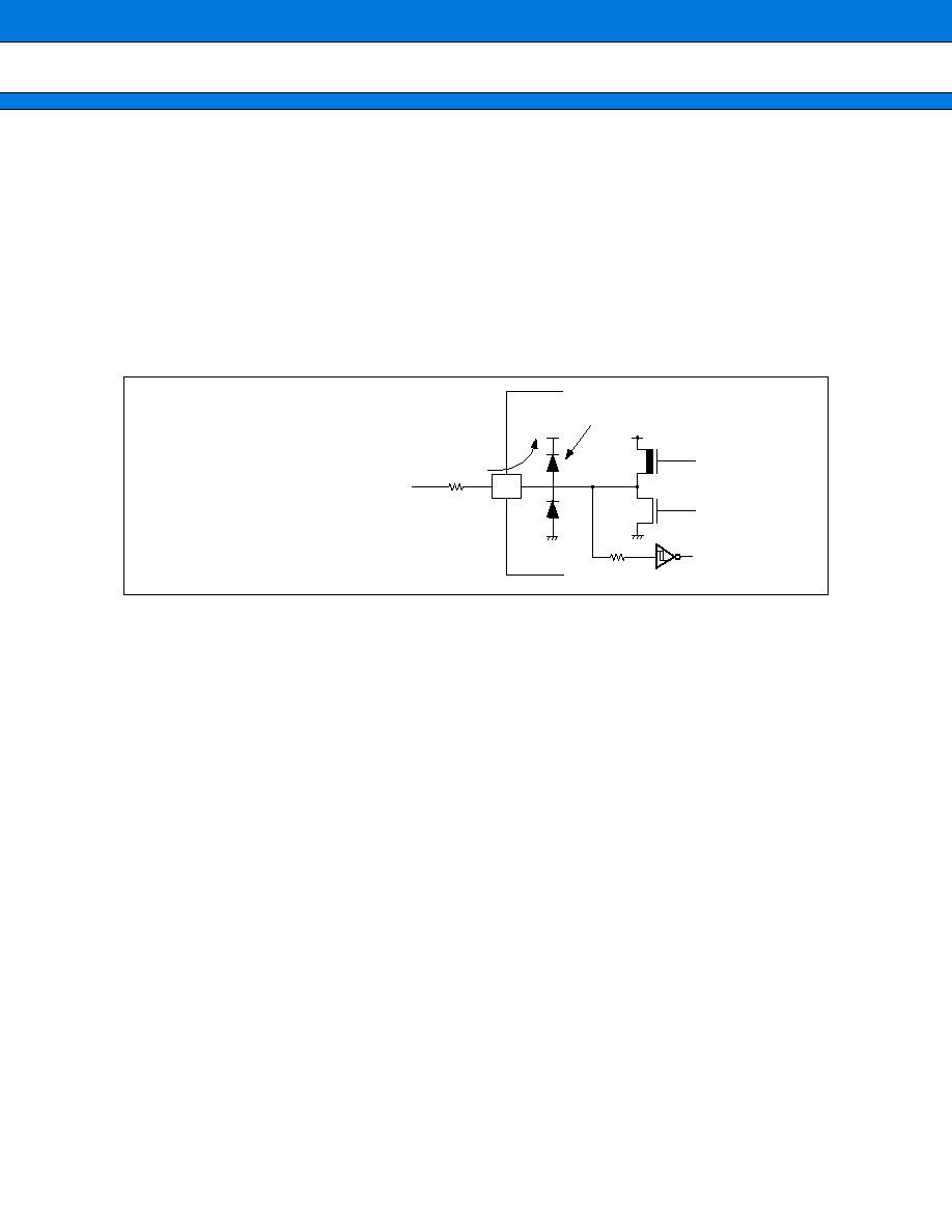
MB90460 Series
64
(Continued)
·
Note that when the microcontroller drive current is low, such as in the power saving modes, the
+
B input
potential may pass through the protective diode and increase the potential at the V
CC
pin, and this may affect
other devices.
·
Note that if a
+
B signal is input when the microcontroller current is off (not fixed at 0 V) , the power supply is
provided from the pins, so that incomplete operation may result.
·
Note that if the
+
B input is applied during power-on, the power supply is provided from the pins and the resulting
supply voltage may not be sufficient to operate the power-on reset.
·
Care must be taken not to leave the
+
B input pin open.
·
Note that analog system input/output pins other than the A/D input pins (LCD drive pins, comparator input
pins, etc.) cannot accept
+
B signal input.
·
Sample recommended circuits:
WARNING: Semiconductor devices can be permanently damaged by application of stress (voltage, current,
temperature, etc.) in excess of absolute maximum ratings. Do not exceed these ratings.
P-ch
N-ch
V
CC
R
· Input/Output Equivalent circuits
+
B input (0 V to 16 V)
Limiting
resistance
Protective diode
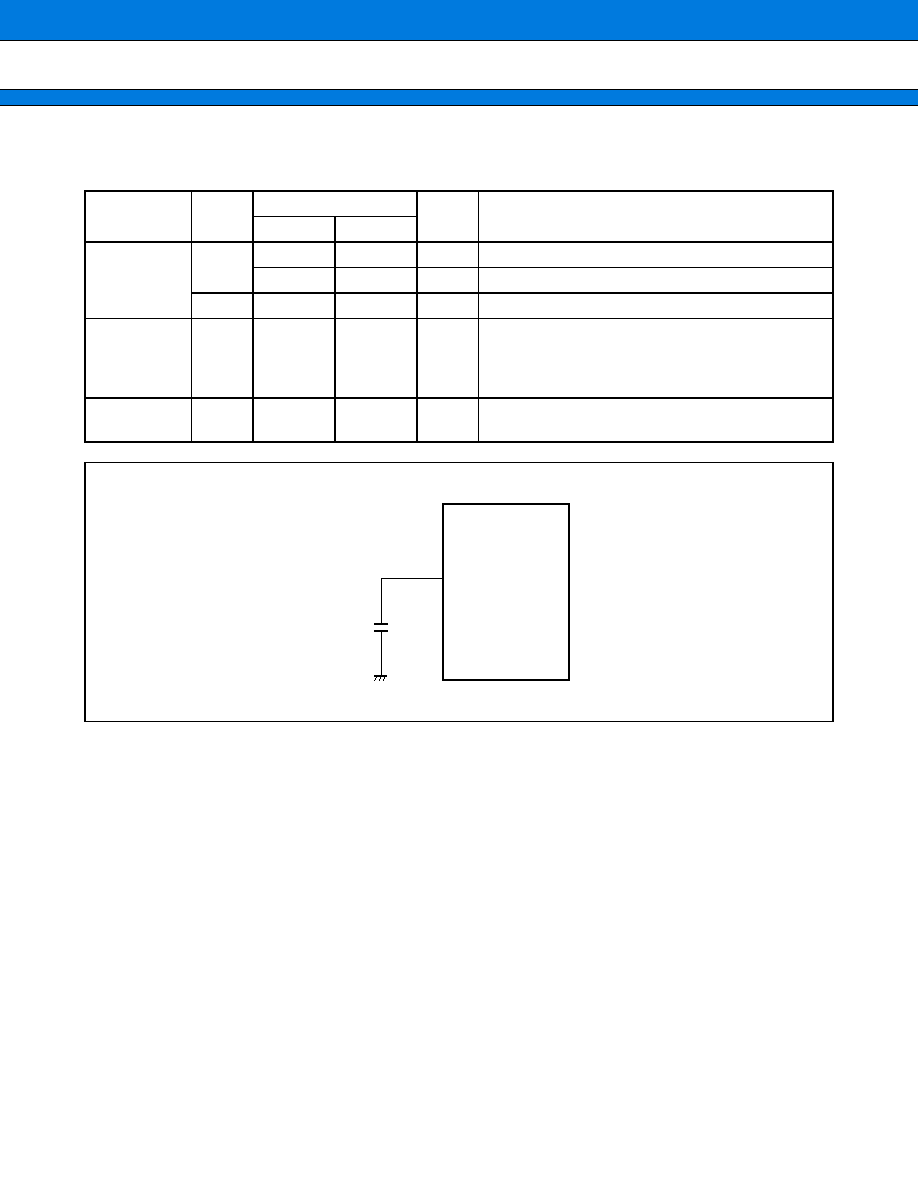
MB90460 Series
65
2.
Recommended Operating Conditions
(V
SS
=
AV
SS
=
0.0 V)
WARNING: The recommended operating conditions are required in order to ensure the normal operation of the
semiconductor device. All of the device's electrical characteristics are warranted when the device is
operated within these ranges.
Always use semiconductor devices within their recommended operating condition ranges. Operation
outside these ranges may adversely affect reliability and could result in device failure.
No warranty is made with respect to uses, operating conditions, or combinations not represented on
the data sheet. Users considering application outside the listed conditions are advised to contact their
FUJITSU representatives beforehand.
Parameter
Sym-
bol
Value
Unit
Remarks
Min
Max
Power supply
voltage
V
CC
3.0
5.5
V
Normal operation (MB90462, MB90467, MB90V460)
4.5
5.5
V
Normal operation (MB90F462)
V
CC
3.0
5.5
V
Retains status at the time of operation stop
Smoothing
capacitor
C
S
0.1
1.0
µ
F
Use a ceramic capacitor or a capacitor with equiva-
lent frequency characteristics. The smoothing capac-
itor to be connected to the V
CC
pin must have a
capacitance value higher than C
S
.
Operating
temperature
T
A
-
40
+
85
°
C
C
C
S
· C pin connection circuit

MB90460 Series
66
3.
DC Characteristics
(V
CC
=
5.0 V
±
10
%
, V
SS
=
AV
SS
=
0.0 V, T
A
=
-
40
°
C to
+
85
°
C)
(Continued)
Parameter
Sym-
bol
Pin name
Condition
Value
Unit
Remarks
Min
Typ
Max
"H" level output
voltage
V
OH
All output pins
V
CC
=
4.5 V,
I
OH
=
-
4.0 mA
V
CC
-
0.5
V
"L" level output
voltage
V
OL
All pins except
P00 to P05 and
P30 to P35
V
CC
=
4.5 V,
I
OL
=
4.0 mA
0.4
V
P00 to P05,
P30 to P35
V
CC
=
4.5 V,
I
OL
=
12.0 mA
0.4
V
"H" level input
voltage
V
IH
P00 to P07
P30 to P37
P50 to P57
V
CC
=
3.0 V to 5.5 V
(MB90462)
V
CC
=
4.5 V to 5.5 V
(MB90F462)
0.7 V
CC
V
CC
+
0.3
V
CMOS input
pin
V
IHS
P10 to P17
P20 to P27
P40 to P46
P60 to P63,
RST
0.8 V
CC
V
CC
+
0.3
V
CMOS hyster-
esis input pin
V
IHM
MD pins
V
CC
-
0.3
V
CC
+
0.3
V
MD pin input
"L" level input
voltage
V
IL
P00 to P07
P30 to P37
P50 to P57
V
SS
-
0.3
0.3 V
CC
V
CMOS input
pin
V
ILS
P10 to P17
P20 to P27
P40 to P46
P60 to P63,
RST
V
SS
-
0.3
0.2 V
CC
V
CMOS hyster-
esis input pin
V
ILM
MD pins
V
SS
-
0.3
V
SS
+
0.3
V
MD pin input
Input leakage
current
I
IL
All input pins
V
CC
=
5.5 V,
V
SS
<
V
I
<
V
CC
-
5
5
µ
A
Power supply
current*
I
CC
V
CC
V
CC
=
5.0 V,
Internal opera-
tion at 16 MHz,
Normal operation
40
50
mA
V
CC
=
5.0 V,
Internal opera-
tion at 16 MHz,
When data writ-
ten in flash mode
programming of
erasing
45
60
mA
I
CCS
V
CC
=
5.0 V,
Internal opera-
tion at 16 MHz,
In sleep mode
15
20
mA

MB90460 Series
67
(Continued)
(V
CC
=
5.0 V
±
10
%
, V
SS
=
AV
SS
=
0.0 V, T
A
=
-
40
°
C to
+
85
°
C)
* : The current value is preliminary value and may be subject to change for enhanced characteristics without previous
notice. The power supply current is measured with an external clock.
Parameter
Sym-
bol
Pin name
Condition
Value
Unit
Remarks
Min
Typ
Max
Power supply
current*
I
CTS
V
CC
V
CC
=
5.0 V,
Internal opera-
tion at 16 MHz,
In Timer mode,
T
A
=
25
°
C
2.5
5.0
mA
I
CCH
In stop mode,
T
A
=
25
°
C
5
20
µ
A
Input
capacitance
C
IN
Except AV
CC
,
AV
SS
, C, V
CC
and V
SS
10
80
pF
Pull-up
resistance
R
UP
P00 to P07
P10 to P17
RST
25
50
100
k
Pull-down
resistance
R
DOWN
MD2
25
50
100
k
MB90460 Series
68
4.
AC Characteristics
(1) Clock Timings
(V
CC
=
5.0 V
±
10
%
, V
SS
=
AV
SS
=
0.0 V, T
A
=
-
40
°
C to
+
85
°
C)
*1 : The frequency fluctuation rate is the maximum deviation rate of the preset center frequency when the multiplied
PLL signal is locked.
*2 : Internal operating clock frequency must not be over 16 MHz.
Parameter
Symbol
Pin
name
Value
Unit
Remarks
Min
Typ
Max
Clock frequency
f
C
X0, X1
3
16
MHz
Crystal oscillator
3
32
External clock *
2
Clock cycle time
t
HCYL
X0, X1
62.5
333
ns
Frequency fluctuation
rate locked*
1
f
5
%
Input clock pulse width
P
WH
P
WL
X0
10
ns
Recommened duty ratio of
30
%
to 70
%
Input clock rise/fall time
t
CR
t
CF
X0
5
ns
External clock operation
Internal operating clock
f
CP
1.5
16
MHz Main clock operation
Internal operating clock
cycle time
t
CP
62.5
666
ns
Main clock operation
+
fo
fo
-
f
=
×
100 (%)
Center
frequency
0.8 V
CC
0.2 V
CC
t
CF
t
CR
t
HCYL
P
WH
P
WL
X0
MB90460 Series
69
The AC ratings are measured for the following measurement reference voltages
Relationship between internal operating clock frequency and power supply voltage
Relationship between oscillating frequency and internal operating clock frequency
5.5
4.5
3.0
3.3
8
Internal clock f
CP
(MHz)
Power supply voltage V
CC
(V)
1
3
12
16
Operation guarantee range of MB90F462
Operation guarantee range of PLL
Operation guarantee range
of MB90462, MB90467, MB90V460
16
12
8
9
4
3
4
8
Oscillation clock f
C
(MHz)
Internal clock f
CP
(MHz)
16
Multiplied-
by-4
Multiplied-
by-3
Multiplied-
by-2
Multiplied-
by-1
Not multiplied
0.8 V
CC
0.2 V
CC
2.4 V
0.8 V
0.7 V
CC
0.3 V
CC
· Input signal waveform
Hysteresis Input Pin
Pin other than hystheresis input/MD input
· Output signal waveform
Output Pin

MB90460 Series
70
(2) Reset Input Timing
(V
CC
=
5.0 V
±
10
%
, V
SS
=
AV
SS
=
0.0 V, T
A
=
-
40
°
C to
+
85
°
C)
* : Oscillation time of oscillator is time that amplitude reached the 90
%
. In the crystal oscillator, the oscillation time
is between several ms to tens of ms. In FAR/ceramic oscillator, the oscillation time is between handreds
µ
s to
several ms. In the external clock, the oscillation time is 0 ms.
Parameter
Symbol
Pin
Condition
Value
Units
Remarks
Min
Max
Reset input time
t
RSTL
RST
4 t
CP
ns
Under normal operation
Oscillation time of
oscillator
+
4 t
CP
*
ms
In stop mode
t
RSTL
0.2 V
CC
0.2 V
CC
4 t
CP
RST
X0
Internal operation clock
Internal reset
90% of
amplitude
Oscillation time of
oscillator
Oscillation setting time
Instruction execution
· In stop mode
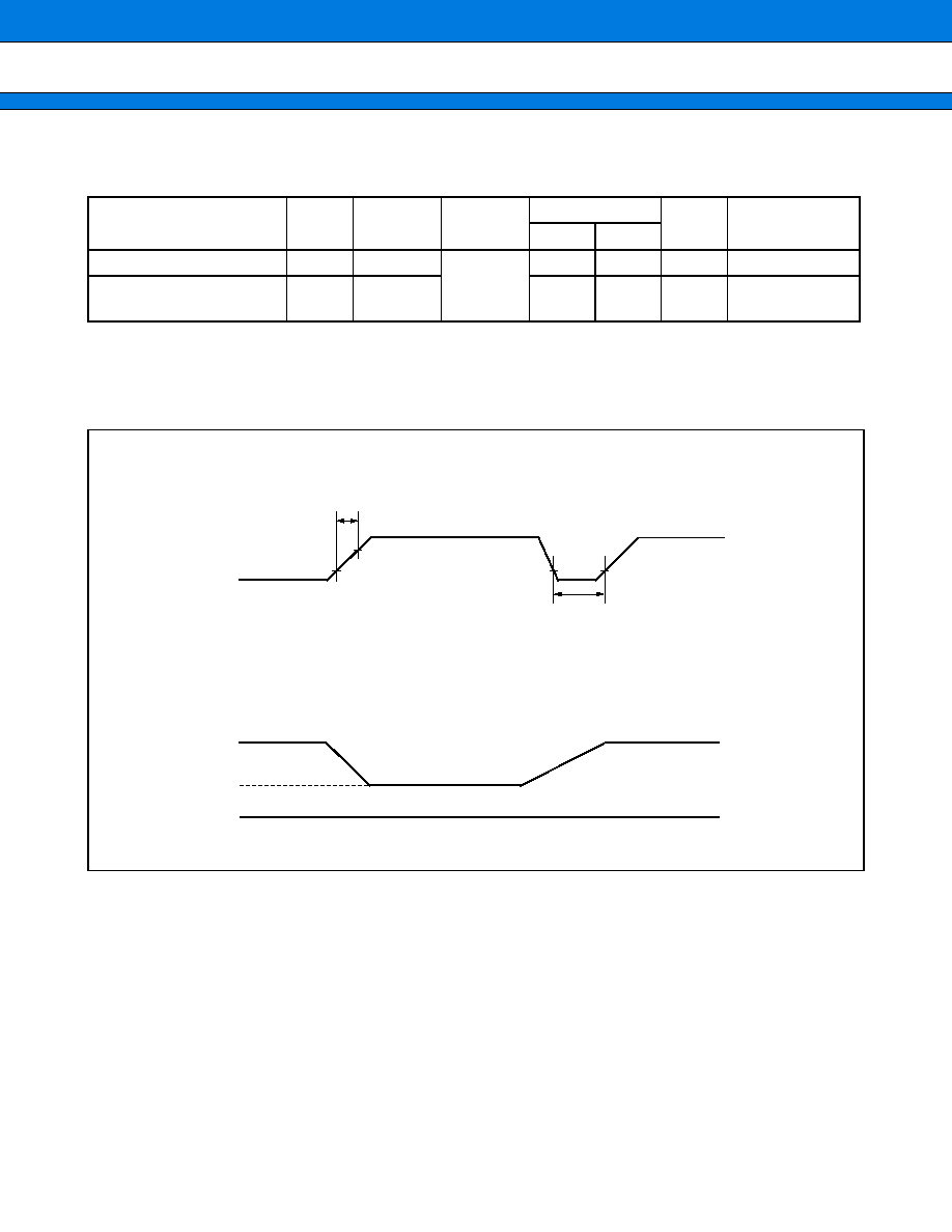
MB90460 Series
71
(3) Power-on Reset
(V
CC
=
5.0 V
±
10
%
, V
SS
=
AV
SS
=
0.0 V, T
A
=
-
40
°
C to
+
85
°
C)
Note : V
CC
must be kept lower than 0.2 V before power-on.
The above values are used for causing a power-on reset.
Some registers in the device are initialized only upon a power-on reset. To initialize these registers, turn the
power supply using the above values.
Parameter
Symbol
Pin name
Condition
Value
Unit
Remarks
Min
Max
Power supply rising time
t
R
V
CC
0.05
30
ms
Power supply cut-off time
t
OFF
V
CC
4
ms
Due to repeated
operations
V
CC
V
CC
V
SS
3.0 V
t
R
t
OFF
2.7 V
0.2 V
0.2 V
0.2 V
RAM data Hold
Sudden changes in the power supply voltage may cause a power-on reset.
To change the power supply voltage while the device is in operation, it is recommended to
raise the voltage smoothly to suppress fluctuations as shown below.
In this case, change the supply voltage with the PLL clock not used. If the voltage drop is 1 V
or fewer per second, however, you can use the PLL clock.
It is recommended to keep the
rising speed of the supply voltage
at 50 mV/ms or slower.
MB90460 Series
72
(4) UART0 to UART1
(V
CC
=
5.0 V
±
10
%
, V
SS
=
AV
SS
=
0.0 V, T
A
=
-
40
°
C to
+
85
°
C)
Note :
·
These are AC ratings in the CLK synchronous mode.
·
CL is the load capacitance value connected to pins while testing.
·
t
CP
is machine cycle time (unit : ns) .
Parameter
Symbol
Pin name
Condition
Value
Unit Remarks
Min
Max
Serial clock cycle time
t
SCYC
SCK0 to SCK1
C
L
=
80 pF
+
1 TTL
for an output pin of
internal shift clock
mode
8 t
CP
ns
SCK
SOT delay time
t
SLOV
SCK0 to SCK1
SOT0 to SOT1
-
80
80
ns
Valid SIN
SCK
t
IVSH
SCK0 to SCK1
SIN0 to SIN1
100
ns
SCK
valid SIN hold time
t
SHIX
SCK0 to SCK1,
SIN0 to SIN1
60
ns
Serial clock "H" pulse width
t
SHSL
SCK0 to SCK1
C
L
=
80 pF
+
1 TTL
for an output pin of
external shift clock
mode
4 t
CP
ns
Serial clock "L" pulse width
t
SLSH
SCK0 to SCK1
4 t
CP
ns
SCK
SOT delay time
t
SLOV
SCK0 to SCK1,
SOT0 to SOT1
150
ns
Valid SIN
SCK
t
IVSH
SCK0 to SCK1,
SIN0 to SIN1
60
ns
SCK
valid SIN hold time
t
SHIX
SCK0 to SCK1,
SIN0 to SIN1
60
ns
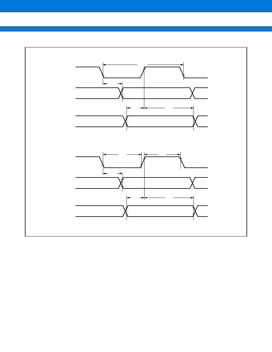
MB90460 Series
73
· Internal shift clock mode
· External shift clock mode
SCK
SOT
SIN
t
SCYC
t
SLOV
t
IVSH
t
SHIX
0.8 V
0.8 V
2.4 V
2.4 V
0.8 V
0.8 V
CC
0.2 V
CC
0.8 V
CC
0.2 V
CC
SCK
SOT
SIN
t
SLSH
t
SHSL
t
SLOV
t
IVSH
t
SHIX
0.2 V
CC
0.2 V
CC
0.8 V
CC
0.8 V
CC
2.4 V
0.8 V
0.8 V
CC
0.2 V
CC
0.8 V
CC
0.2 V
CC
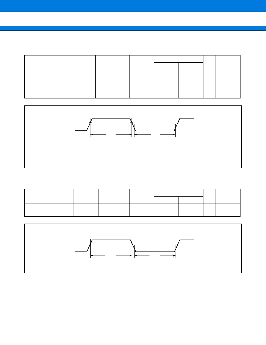
MB90460 Series
74
(5) Resources Input Timing
(V
CC
=
5.0 V
±
10
%
, V
SS
=
AV
SS
=
0.0 V, T
A
=
-
40
°
C to
+
85
°
C)
(6) Trigger Input Timimg
(V
CC
=
5.0 V
±
10
%
, V
SS
=
AV
SS
=
0.0 V, T
A
=
-
40
°
C to
+
85
°
C)
Parameter
Symbol
Pin name
Condition
Value
Unit
Remarks
Min
Max
Input pulse width
t
TIWH
t
TIWL
IN0 to IN3,
SNI0 to SNI2
TIN0 to TIN1
PWI0 to PWI1
DTTI0, DTTI1
4 t
CP
ns
Parameter
Symbol
Pin name
Condition
Value
Unit
Remarks
Min
Max
Input pulse width
t
TRGH
t
TRGL
INT0 to INT7
5 t
CP
ns
0.8 V
CC*1
0.8 V
CC
0.2 V
CC*2
0.2 V
CC*2
t
TIWH
t
TIWL
*1 : 0.7 V
CC
for PWI0 input pin
*2 : 0.3 V
CC
for PWI0 Input pin
0.8 V
CC
0.8 V
CC
0.2 V
CC
0.2 V
CC
t
TRGH
t
TRGL
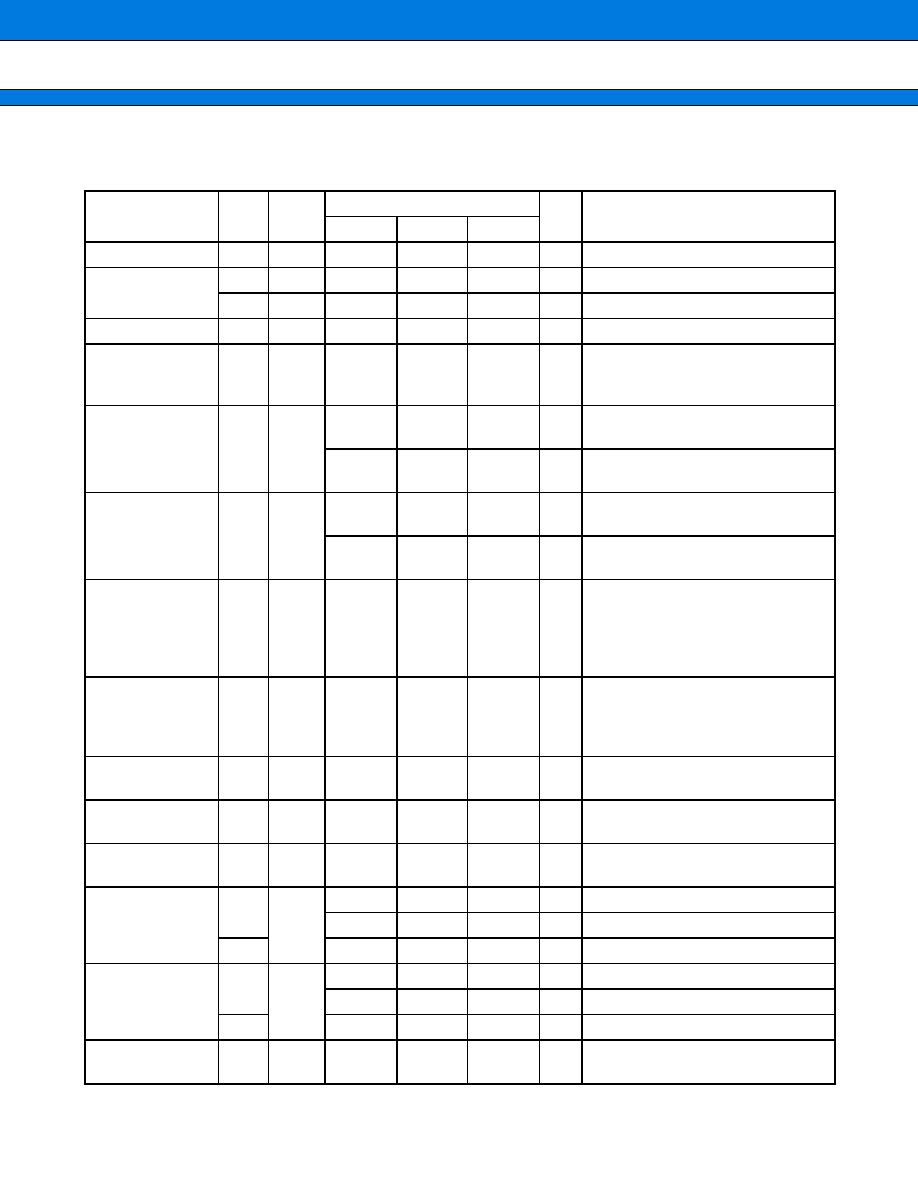
MB90460 Series
75
5.
A/D Converter Electrical Characteristics
(3.0 V
AVR
-
AV
SS
, V
CC
=
AV
CC
=
5.0 V
±
10
%
, V
SS
=
AV
SS
=
0.0 V, T
A
=
-
40
°
C to
+
85
°
C)
* : The current when the A/D converter is not operating or the CPU is in stop mode (for V
CC
=
AV
CC
=
AVR
=
5.0 V)
Parameter
Sym-
bol
Pin
name
Value
Unit
Remarks
Min
Typ
Max
Resolution
10
bit
Total error
±
3.0
LSB For MB90F462, MB90462, MB90467
±
5.0
LSB For MB90V460
Non-linear error
±
2.5
LSB
Differential
linearity
error
±
1.9
LSB
Zero transition
voltage
V
OT
AN0 to
AN7
AV
SS
-
1.5 LSB
AV
SS
+
0.5 LSB
AV
SS
+
2.5 LSB
mV
For MB90F462, MB90462, MB90467
AV
SS
-
3.5 LSB
AV
SS
+
0.5 LSB
AV
SS
+
4.5 LSB
mV
For MB90V460
Full-scale
transition
voltage
V
FST
AN0 to
AN7
AVR
-
3.5 LSB
AVR
-
1.5 LSB
AVR
+
0.5 LSB
mV
For MB90F462, MB90462, MB90467
AVR
-
6.5 LSB
AVR
-
1.5 LSB
AVR
+
1.5 LSB
mV
For MB90V460
Conversion time
6.125
1000
µ
s
Actual value is specified as a sum of
values specified in ADCR0 : CT1,
CT0 and ADCR0 : ST1, ST0. Be sure
that the setting value is greater than
the min value
Sampling period
2
µ
s
Actual value is specified in ADCR0 :
ST1, ST0 bits. Be sure that the set-
ting value is greater than the min val-
ue
Analog port input
current
I
AIN
AN0 to
AN7
10
µ
A
Analog input
voltage
V
AIN
AN0 to
AN7
AV
SS
AVR
V
Reference voltage
AVR
AV
SS
+
2.7
AV
CC
V
Power supply
current
I
A
AV
CC
2.3
6
mA
For MB90F462, MB90462, MB90467
2
5
mA
For MB90V460
I
AH
*
5
µ
A
*
Reference voltage
supply current
IR
AVR
140
260
µ
A
For MB90F462, MB90462, MB90467
0.9
1.3
mA
For MB90V460
I
RH
*
5
µ
A
*
Offset between
channels
AN0 to
AN7
4
LSB
MB90460 Series
76
6.
A/D Converter Glossary
(Continued)
Resolution :
Analog changes that are identifiable with the A/D converter
Linearity error :
The deviation of the straight line connecting the zero transition point
("00 0000 0000"
"000000 0001") with the full-scale transition point
("11 1111 1110"
"11 1111 1111") from actual conversion characteristics
Differential linearity error : The deviation of input voltage needed to change the output code by 1 LSB from the
theoretical value
Total error :
The total error is defined as a difference between the actual value and the theoretical
value, which includes zero-transition error/full-scale transition error and linearity error.
3FF
3FE
3FD
004
003
002
001
AVss
Digital output
AVR
Analog input
1.5 LSB
0.5 LSB
{1 LSB
×
(N
-
1)
+
0.5 LSB}
Actual conversion
value
Actual conversion
value
Theoretical
characteristics
V
NT
(Measured value)
Total error
Total error for digital output N
=
V
NT
-
{1 LSB
×
(N
-
1)
+
0.5 LSB}
[LSB]
1 LSB
1 LSB
=
(Theoretical value)
AVR
-
AV
SS
[V]
1024
V
OT
(Theoretical value)
=
AV
SS
+
0.5 LSB [V]
V
FST
(Theoretical value)
=
AVR
-
1.5 LSB [V]
V
NT
: Voltage at a transition of digital output from (N
-
1) to N
MB90460 Series
77
(Continued)
3FF
3FE
3FD
004
003
002
001
AVss
AVR
AVss
AVR
N
+
1
N
N
-
1
N
-
2
V
NT
V
(
N
+
1) T
V
OT
(Measured value)
V
FST
{1 LSB
×
(N
-
1)
+
V
OT
}
Digital output
Digital output
Analog input
Analog input
Actual conversion
value
(Measured
value)
Actual conversion
value
Theoretical
characteristics
(measured value)
Theoretical
characteristics
Actual conversion
value
(Measured value)
Actual conversion
value
V
NT
(Measured value)
Differential linearity error
Linearity error
Linearity error of
digital output N
V
NT
-
{1 LSB
×
(N
-
1)
+
V
OT
}
=
1 LSB
[LSB]
Differential linearity error
of digital output N
V (
N
+
1
)
T
-
V
NT
=
1 LSB
-
1 [LSB]
V
FST
-
V
OT
=
1022
[V]
1 LSB
V
OT
: Voltage at transition of digital output from "000
H
" to "001
H
"
V
FST
: Voltage at transition of digital output from "3FE
H
" to "3FF
H
"
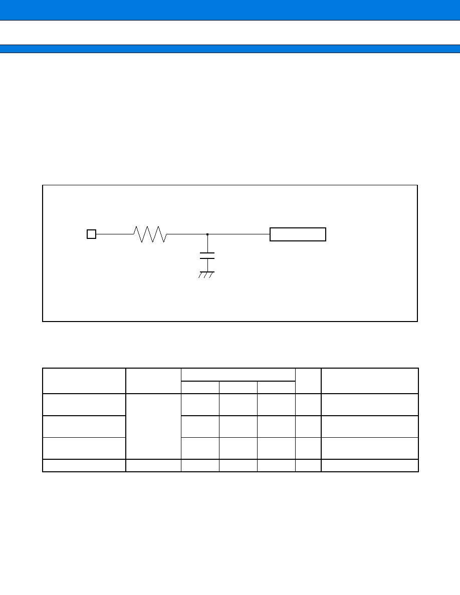
MB90460 Series
78
7.
Notes on Using A/D Converter
Select the output impedance value for the external circuit of analog input according to the following conditions.
Output impedance values of the external circuit recommends about 5 k
or lower (sampling period
=
2.0
µ
s
@machine clock of 16 MHz) .
When capacitors are connected to external pins, the capacitance of several thousand times the internal capacitor
value is recommended to minimized the effect of voltage distribution between the external capacitor and internal
capacitor.
When the output impedance of the external circuit is too high, the sampling period for analog voltages may not
be sufficient.
· Error
The smaller the absolute value of | AVR
-
AV
SS
|, the greater the error would become relatively.
8.
Flash Memory Program and Erase Performances
Parameter
Condition
Value
Unit
Remarks
Min
Typ
Max
Sector erase time
T
A
=
+
25
°
C
V
CC
=
3.0 V
1
15
s
Excludes 00H programming
prior erasure
Chip erase time
5
s
Excludes 00 H program-
ming prior erasure
Word (16 bit width)
programming time
16
3,600
µ
s
Excludes
system-level overhead
Erase/Program cycle
10,000
cycle
C
Comparator
Analog input
R
· Analog input circuit model
Note : Listed values must be considered as standards.
MB90462, MB90F462, MB90467 R
2.6 K
, C
28 pF
MB90V460
R
3.2 K
, C
30 pF
MB90460 Series
79
s
s
s
s
EXAMPLE CHARACTERISTICS
· Power Suppy Current of MB90462, MB90467
40
35
30
25
20
15
10
5
0
2
3
4
5
6
I
CCH
(mA)
F
C
=
16 [MHz]
F
C
=
12 [MHz]
F
C
=
10 [MHz]
F
C
=
8 [MHz]
F
C
=
4 [MHz]
F
C
=
2 [MHz]
V
CC
(V)
I
CCS
(mA)
2
3
4
5
6
F
C
=
4 [MHz]
F
C
=
12 [MHz]
F
C
=
16 [MHz]
F
C
=
10 [MHz]
F
C
=
8 [MHz]
F
C
=
2 [MHz]
20
18
16
14
12
10
8
6
4
2
0
V
CC
(V)
V
CC
-
V
OH
(mV)
I
OH
(mA)
1000
900
800
700
600
500
400
300
200
100
0
0
2
4
6
8
10
12
-
-
-
-
-
-
V
OL
(V)
I
OL
(mA)
1000
900
800
700
600
500
400
300
200
100
0
0
2
4
6
8
10
12
I
CCH
vs. V
CC
T
A
=
25
°
C, external clock input
I
CCS
vs. V
CC
T
A
=
25
°
C, external clock input
V
CC
-
V
OH
vs. I
OH
T
A
=
25
°
C, V
CC
=
4.5 V
V
OL
vs. I
OL
T
A
=
25
°
C, V
CC
=
4.5 V
MB90460 Series
80
· Power Suppy Current of MB90F462
40
35
30
25
20
15
10
5
0
2
3
4
5
6
I
CCH
(mA)
F
C
=
16 [MHz]
F
C
=
12 [MHz]
F
C
=
10 [MHz]
F
C
=
8 [MHz]
F
C
=
4 [MHz]
F
C
=
2 [MHz]
V
CC
(V)
I
CCS
(mA)
2
3
4
5
6
F
C
=
4 [MHz]
F
C
=
12 [MHz]
F
C
=
10 [MHz]
F
C
=
8 [MHz]
F
C
=
2 [MHz]
20
18
16
14
12
10
8
6
4
2
0
F
C
=
16 [MHz]
V
CC
(V)
V
CC -
V
OH
(mV)
I
OH
(mA)
1000
900
800
700
600
500
400
300
200
100
0
0
2
4
6
8
10
12
V
OL
(V)
I
OL
(mA)
1000
900
800
700
600
500
400
300
200
100
0
0
2
4
6
8
10
12
I
CCH
vs. V
CC
T
A
=
25
°
C, external clock input
I
CCS
vs. V
CC
T
A
=
25
°
C, external clock input
V
CC
-
V
OH
vs. I
OH
T
A
=
25
°
C, V
CC
=
4.5 V
V
OL
vs. I
OL
T
A
=
25
°
C, V
CC
=
4.5 V

MB90460 Series
81
s
s
s
s
ORDERING INFORMATION
Part number
Package
Remarks
MB90F462PFM
MB90462PFM
MB90467PFM
64-pin Plastic LQFP
(FPT-64P-M09)
MB90F462PF
MB90462PF
MB90467PF
64-pin Plastic QFP
(FPT-64P-M06)
MB90F462P-SH
MB90462P-SH
MB90467P-SH
64-pin Plastic SH-DIP
(DIP-64P-M01)
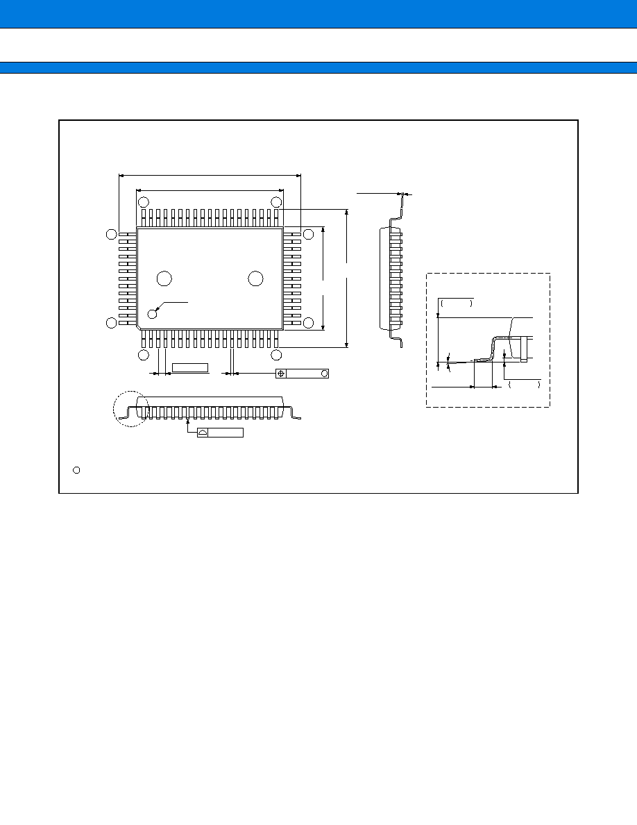
MB90460 Series
82
s
s
s
s
PACKAGE DIMENSIONS
64-pin Plastic QFP
(FPT-64P-M06)
Note : Pins width and pins thickness include plating thickness.
Dimensions in mm (inches)
C
2001 FUJITSU LIMITED F64013S-c-4-4
0.20(.008)
M
18.70±0.40
(.736±.016)
14.00±0.20
(.551±.008)
1.00(.039)
INDEX
0.10(.004)
1
19
20
32
52
64
33
51
20.00±0.20(.787±.008)
24.70±0.40(.972±.016)
0.42±0.08
(.017±.003)
0.17±0.06
(.007±.002)
0~8°
1.20±0.20
(.047±.008)
3.00
+0.35
0.20
(Mounting height)
.118
+.014
.008
0.25
+0.15
0.20
.010
+.006
.008
(Stand off)
Details of "A" part
"A"
0.10(.004)
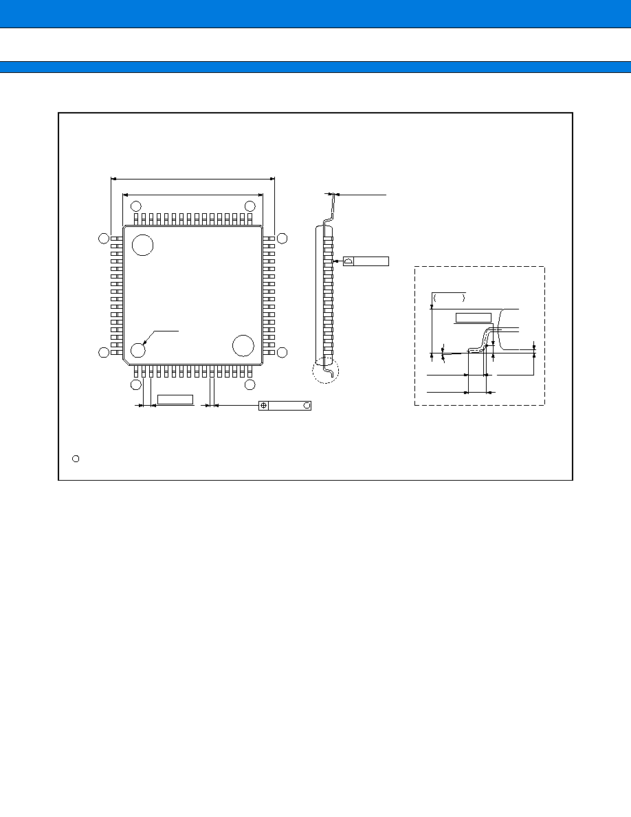
MB90460 Series
83
64-pin Plastic LQFP
(FPT-64P-M09)
Note : Pins width and pins thickness include plating thickness.
Dimensions in mm (inches)
C
2001 FUJITSU LIMITED F64018S-c-2-4
0.65(.026)
0.10(.004)
1
16
17
32
49
64
33
48
12.00±0.10(.472±.004)SQ
14.00±0.20(.551±.008)SQ
INDEX
0.32±0.05
(.013±.002)
M
0.13(.005)
0.145±0.055
(.0057±.0022)
"A"
.059
.004
+.008
0.10
+0.20
1.50
0~8°
0.25(.010)
(Mounting height)
0.50±0.20
(.020±.008)
0.60±0.15
(.024±.006)
0.10±0.10
(.004±.004)
Details of "A" part
(Stand off)
0.10(.004)
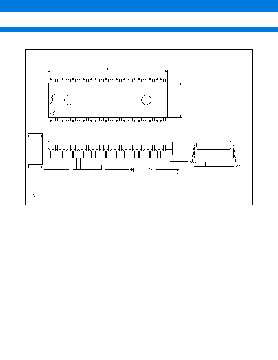
MB90460 Series
84
64-pin Plastic SH-DIP
(DIP-64P-M01)
Note : Pins width and pins thickness include plating thickness.
Dimensions in mm (inches)
C
2001 FUJITSU LIMITED D64001S-c-4-5
58.00
+0.22
0.55
+.009
.022
2.283
17.00±0.25
(.669±.010)
3.30
+0.20
0.30
.130
.012
+.008
+.028
.008
.195
0.20
+0.70
4.95
+.016
.008
.0543
0.20
+0.40
1.378
1.778(.0700)
0.47±0.10
(.019±.004)
1.00
+0.50
0
.039
.0
+.020
+.020
.007
.028
0.19
+0.50
0.70
19.05(.750)
(.011±.004)
0.27±0.10
0~15°
INDEX-2
INDEX-1
M
0.25(.010)

MB90460 Series
FUJITSU LIMITED
For further information please contact:
Japan
FUJITSU LIMITED
Marketing Division
Electronic Devices
Shinjuku Dai-Ichi Seimei Bldg. 7-1,
Nishishinjuku 2-chome, Shinjuku-ku,
Tokyo 163-0721, Japan
Tel: +81-3-5322-3353
Fax: +81-3-5322-3386
http://edevice.fujitsu.com/
North and South America
FUJITSU MICROELECTRONICS AMERICA, INC.
3545 North First Street,
San Jose, CA 95134-1804, U.S.A.
Tel: +1-408-922-9000
Fax: +1-408-922-9179
Customer Response Center
Mon. - Fri.: 7 am - 5 pm (PST)
Tel: +1-800-866-8608
Fax: +1-408-922-9179
http://www.fma.fujitsu.com/
Europe
FUJITSU MICROELECTRONICS EUROPE GmbH
Am Siebenstein 6-10,
D-63303 Dreieich-Buchschlag,
Germany
Tel: +49-6103-690-0
Fax: +49-6103-690-122
http://www.fme.fujitsu.com/
Asia Pacific
FUJITSU MICROELECTRONICS ASIA PTE. LTD.
#05-08, 151 Lorong Chuan,
New Tech Park,
Singapore 556741
Tel: +65-281-0770
Fax: +65-281-0220
http://www.fmal.fujitsu.com/
Korea
FUJITSU MICROELECTRONICS KOREA LTD.
1702 KOSMO TOWER, 1002 Daechi-Dong,
Kangnam-Gu,Seoul 135-280
Korea
Tel: +82-2-3484-7100
Fax: +82-2-3484-7111
F0112
©
FUJITSU LIMITED Printed in Japan
All Rights Reserved.
The contents of this document are subject to change without notice.
Customers are advised to consult with FUJITSU sales
representatives before ordering.
The information and circuit diagrams in this document are
presented as examples of semiconductor device applications, and
are not intended to be incorporated in devices for actual use. Also,
FUJITSU is unable to assume responsibility for infringement of
any patent rights or other rights of third parties arising from the use
of this information or circuit diagrams.
The products described in this document are designed, developed
and manufactured as contemplated for general use, including
without limitation, ordinary industrial use, general office use,
personal use, and household use, but are not designed, developed
and manufactured as contemplated (1) for use accompanying fatal
risks or dangers that, unless extremely high safety is secured, could
have a serious effect to the public, and could lead directly to death,
personal injury, severe physical damage or other loss (i.e., nuclear
reaction control in nuclear facility, aircraft flight control, air traffic
control, mass transport control, medical life support system, missile
launch control in weapon system), or (2) for use requiring
extremely high reliability (i.e., submersible repeater and artificial
satellite).
Please note that Fujitsu will not be liable against you and/or any
third party for any claims or damages arising in connection with
above-mentioned uses of the products.
Any semiconductor devices have an inherent chance of failure. You
must protect against injury, damage or loss from such failures by
incorporating safety design measures into your facility and
equipment such as redundancy, fire protection, and prevention of
over-current levels and other abnormal operating conditions.
If any products described in this document represent goods or
technologies subject to certain restrictions on export under the
Foreign Exchange and Foreign Trade Law of Japan, the prior
authorization by Japanese government will be required for export
of those products from Japan.
Document Outline