
DS04-13105-2E
FUJITSU SEMICONDUCTOR
DATA SHEET
Linear IC Converter
CMOS
A/D Converter
(With 4-channel Input at 12-bit Resolution)
MB88101A
s
DESCRIPTION
The MB88101A is an analog-to-digital converter that converts its analog input to a 12-bit digital value and outputs
it as serial data.
The MB88101A employs a successive approximation method for A/D conversion.
The MB88101A has four input channels selectable for analog input under control of the dedicated external pins.
The MB88101A can be switched to a mode for continuous A/D conversion, in which it outputs serial data from the
MSB or LSB selectable depending on the mode setting.
s
FEATURES
· 4-channel analog input
· One analog input channel selectable for conversion by external control
· CR-type successive approximation system with a sample-and-hole circuit
· 12-bit resolution
· Serial output of 12-bit digital data
· Capable of continuous conversion (continuous conversion mode)
· MSB or LSB selectable for serial output
· CMOS process
· Package options of 16-pin DIP, SSOP, and SOP available
s
PACKAGES
16-pin Plastic DIP
(DIP-16P-M04)
16-pin Plastic SSOP
(FPT-16P-M05)
16-pin Plastic SOP
(FPT-16P-M06)

3
MB88101A
s
PIN DESCRIPTION
Pin no.
Symbol
I/O
Descriptions
1
2
5
6
AN
0
AN
1
AN
2
AN
3
I
Analog input pins. One of these channels can be selected depending on
the C
0
and C
1
settings.
14
DO
O
This pin outputs the result of A/D conversion. The result is 12-bit serial
data output in synchronization with the rise of CLK.
13
CLK
I
Clock input pin for A/D conversion
12
CS
I
Chip select signal input pin. Setting the signal level to "L" after turning
the power on starts A/D conversion; setting it to "H" stops A/D
conversion. When this pin is "H", the DO and SAMP pins are "Hi-z".
11
10
C
0
C
1
I
Input pins for selecting the analog input channels from among pins AN
0
to AN
3
. See Table 1 for the correspondence between the pin settings
and the channels selected. To switch the channel in mode 2 or 3, set
these pins before the SAMP pin goes "H".
7
8
MOD0
MOD1
I
Conversion mode setting pins. For the correspondence between the pin
settings and the modes selected, see Table 2 and "
s
FUNCTIONAL
DESCRIPTION."
15
SAMP
O
This pin becomes active in prior to data output. Serial data is output from
the DO pin three clock cycles after the signal level at this pin goes "L"
after "H" for one clock cycle.
3
V
REF
--
Reference voltage input pin
4
A
GND
--
Analog circuit ground pin
9
D
GND
--
Digital circuit ground pin
16
V
CC
--
Power supply pin
C
1
C
0
Channel
MOD 0
MOD1
Mode
L
L
AN
0
L
L
Mode 1
L
H
AN
1
L
H
Mode 2
H
L
AN
2
H
L
(Disabled)
H
H
AN
3
H
H
Mode 3
· Channel selection
· Mode selection
Table 1 Pin Settings and Channel Selection
Table 2 Pin Settings and Mode Selection
5
MB88101A
s
FUNCTIONAL DESCRIPTION
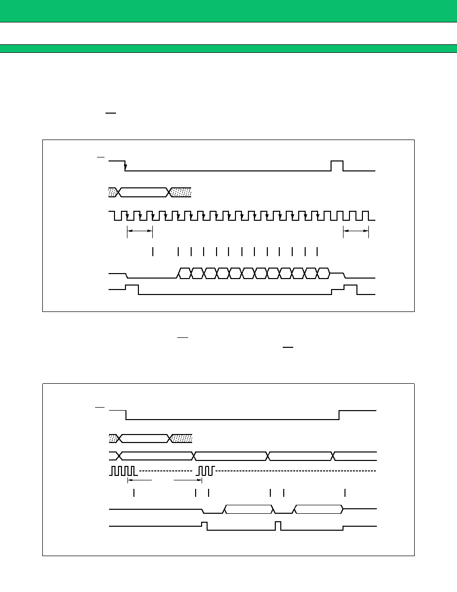
1. Mode 1
This mode sets the DO pin to "L" and stops conversion upon completion of conversion of 12 bits. To restart
conversion, set CS to "H" once then to "L". In this mode, converted data is output from the MSB.
· Timing diagram
2. Mode 2
This mode continues conversion until CS becomes "H" after it becomes "L". Converted data is output from the
LSB, with the first piece of converted data output 20 clock cycles after CS becomes "L". Changing the channel
select pin settings before starting sampling of one analog input allows another to be converted.
· Timing diagram
CLK
CS
MOD0, 1
C
0
, C
1
DO
Bit
Trial
SAMP
B11
B11
B10 B9 B8 B7 B6 B5 B4 B3 B2 B1 B0
B10 B9
B8
B7
B6
B5
B4
B3
B2
B1
B0
Sampling
Sampling
1
2
3
4
5
6
7
8
9
10 11 12 13 14 15 16
1
2
Hi-z
Hi-z
Hi-z
Hi-z
CS
MOD0, 1
MOD0, 1
Mode 2
C
0
, C
1
AN
0
AN
2
AN
1
CLK
DO
Bit
Trial
SAMP
Hi-z
Hi-z
Hi-z
Hi-z
16CLK
MSB (AN
0
)
LSB
MSB (AN
2
)
LSB
LSB (AN
0
)
MSB
LSB (AN
2
)
MSB
MSB (AN
1
)
LSB

