DS05-50204-2E
FUJITSU SEMICONDUCTOR
DATA SHEET
Stacked MCP (Multi-Chip Package) FLASH MEMORY & SRAM
CMOS
32M (
×
8/
×
16) FLASH MEMORY &
4M (
×
8/
×
16) STATIC RAM
MB84VD2218XEC
-90
/MB84VD2219XEC
-90
MB84VD2218XEE
-90
/MB84VD2219XEE
-90
s
s
s
s
FEATURES
· Power supply voltage of 2.7 to 3.3 V
· High performance
90 ns maximum access time (Flash)
85 ns maximum access time (SRAM)
· Operating Temperature
25 to +85
°
C
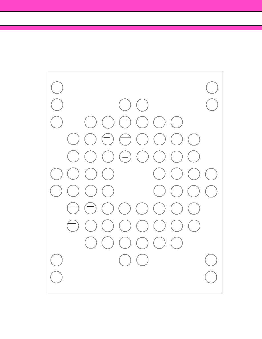
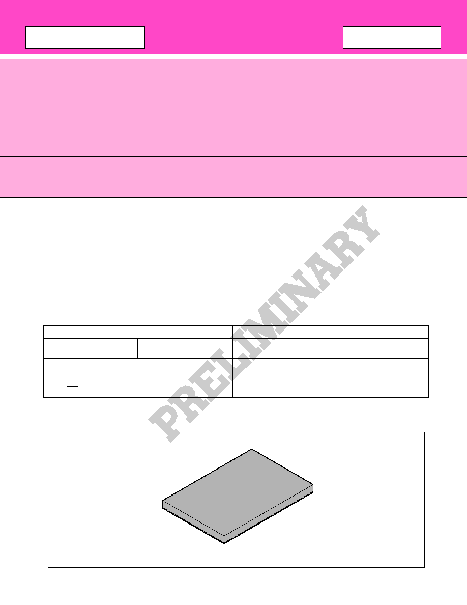
· Package 73-ball BGA
(Continued)
s
s
s
s
PRODUCT LINE UP
s
s
s
s
PACKAGE
Flash Memory
SRAM
Ordering Part No.
V
CC
f, V
CC
s = 3.0 V
MB84VD2218XEC/EE-90/MB84VD2219XEC/EE-90
Max. Address Access Time (ns)
90
85
Max. CE Access Time (ns)
90
85
Max. OE Access Time (ns)
40
45
+0.3 V
0.3 V
73-ball plastic BGA
(BGA-73P-M01)

MB84VD2218XEC/EE/2219XEC/EE
-90
2
(Continued)
1.FLASH MEMORY
· Simultaneous Read/Write operations (dual bank)
Miltiple devices available with different bank sizes
Host system can program or erase in one bank, then immediately and simultaneously read from the other bank
Zero latency between read and write operations
Read-while-erase
Read-while-program
· Minimum 100,000 write/erase cycles
· Sector erase architecture
Eight 4 K words and sixty three 32 K words.
Any combination of sectors can be concurrently erased. Also supports full chip erase.
· Boot Code Sector Architecture
MB84VD2218X: Top sector
MB84VD2219X: Bottom sector
· Embedded Erase
TM
Algorithms
Automatically pre-programs and erases the chip or any sector
· Embedded Program
TM
Algorithms
Automatically writes and verifies data at specified address
· Data Polling and Toggle Bit feature for detection of program or erase cycle completion
· Ready-Busy output (RY/BY)
Hardware method for detection of program or erase cycle completion
· Automatic sleep mode
When addresses remain stable, automatically switch themselves to low power mode.
· Low V
CC
f write inhibit
2.5 V
· Hidden ROM (Hi-ROM) region
64K byte of Hi-ROM, accessible through a new "Hi-ROM Enable" command sequence
Factory serialized and protected to provide a secure electronic serial number (ESN)
· WP/ACC input pin
At V
IL
, allows protection of boot sectors, regardless of sector protection/unprotection status
(MB84VD2218XEC/EE:SA69,SA70 MB84VD2219XEC/EE:SA0,SA1)
At V
IH
, allows removal of boot sector protection
At V
ACC
, program time will reduse by 40%.
· Erase Suspend/Resume
Suspends the erase operation to allow a read in another sector within the same device
· Please refer to "MBM29DL32XTE/BE" data sheet in detailed function
2.SRAM
· Power dissipation
Operating : 50 mA max.
Standby : 15
µ
A max.
· Power down features using CE1s and CE2s
· Data retention supply voltage: 1.5 V to 3.3 V
· CE1s and CE2s Chip Select
· Byte data control: LBs(DQ
0
-DQ
7
), UBs(DQ
8
-DQ
15
)
MB84VD2218XEC/EE/2219XEC/EE
-90
4
s
s
s
s
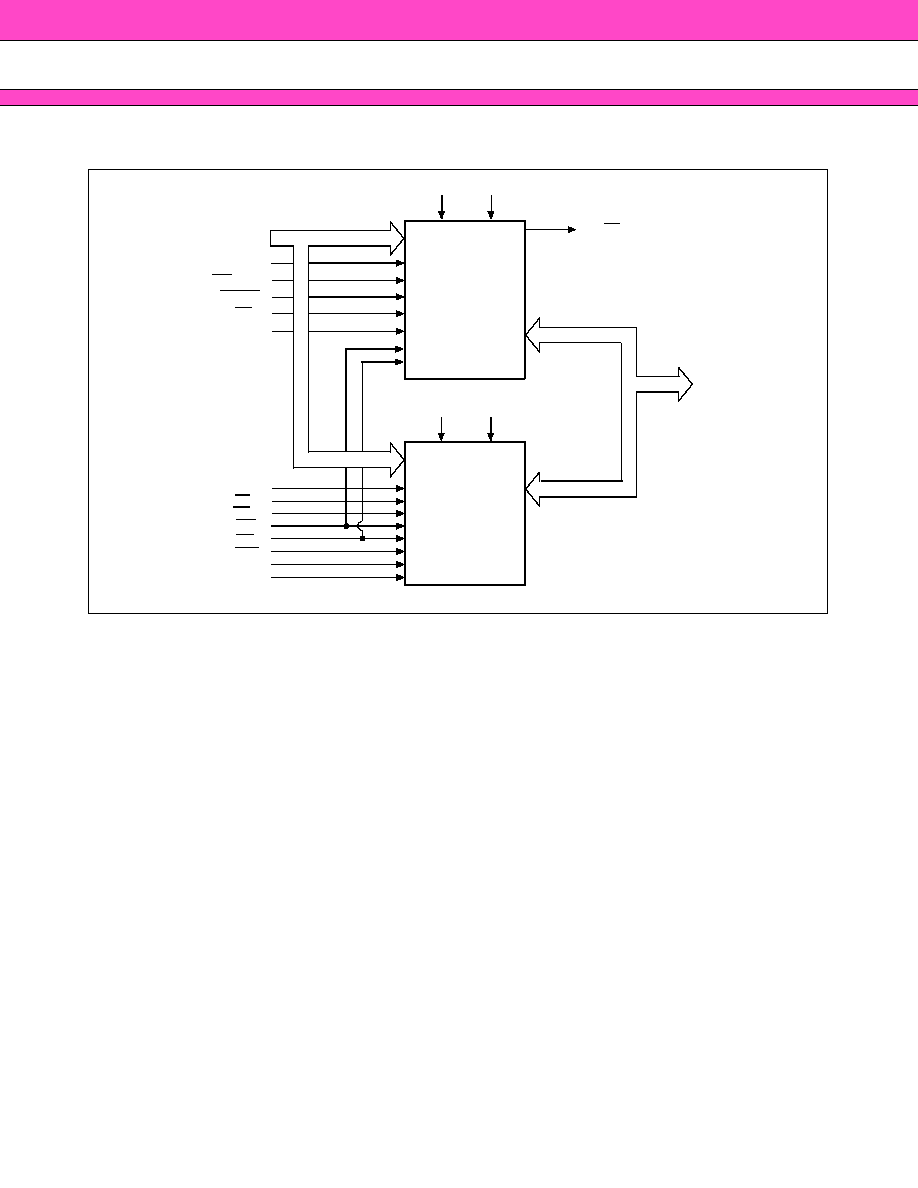
PIN DESCRIPTION
Pin Name
Function
Input/Output
A
0
to A
17
Address Inputs (Common)
I
A
1
, A
18
to A
20
Address Input (Flash)
I
SA
Address Input (SRAM)
I
DQ
0
to DQ
15
Data Inputs/Outputs (Common)
I/O
CEf
Chip Enable (Flash)
I
CE1s
Chip Enable (SRAM)
I
CE2s
Chip Enable (SRAM)
I
OE
Output Enable (Common)
I
WE
Write Enable (Common)
I
RY/BY
Ready/Busy Outputs (Flash) Open Drain Output
O
UBs
Upper Byte Control (SRAM)
I
LBs
Lower Byte Control (SRAM)
I
CIOf
I/O Configuration (Flash)
CIOf = V
IH
is Word mode (×16), CIOf = V
IL
is Byte mode (×8)
I
CIOs
I/O Configuration (SRAM)
CIOs = V
IH
is Word mode (×16), CIOs = V
IL
is Byte mode (×8)
I
RESET
Hardware Reset Pin/Sector Protection Unlock (Flash)
I
WP/ACC
Write Protect / Acceleration (Flash)
I
N.C.
No Internal Connection
--
V
SS
Device Ground (Common)
Power
V
CC
f
Device Power Supply (Flash)
Power
V
CC
s
Device Power Supply (SRAM)
Power