DS05-50111-1E
FUJITSU SEMICONDUCTOR
DATA SHEET
MCP (Multi-Chip Package) FLASH MEMORY & SRAM
CMOS
8M (
ū
16) FLASH MEMORY &
2M (
ū
16) STATIC RAM
MB84VD2008
-10
/MB84VD2009
-10
s
FEATURES
Ę Power supply voltage of 2.7 to 3.6 V
Ę High performance
100 ns maximum access time
Ę Operating Temperature
Ł20 to +85
░
C
-- FLASH MEMORY
Ę Simultaneous operations Read-while Erase or Read-while-Program
Ę Minimum 100,000 write/erase cycles
Ę Sector erase architecture
Two 16 K byte, four 8 K bytes, two 32 K byte, and fourteen 64 K bytes.
Any combination of sectors can be concurrently erased. Also supports full chip erase.
Ę Boot Code Sector Architecture
MB84VD2008: Top sector
MB84VD2009: Bottom sector
Ę Embedded Erase
TM
Algorithms
Automatically pre-programs and erases the chip or any sector
Ę Embedded Program
TM
Algorithms
Automatically writes and verifies data at specified address
Ę Data Polling and Toggle Bit feature for detection of program or erase cycle completion
Ę Ready-Busy output (RY/BY)
Hardware method for detection of program or erase cycle completion
Ę Automatic sleep mode
When addresses remain stable, automatically switch themselves to low power mode.
Ę Low V
CC
write inhibit
2.5 V
Ę Erase Suspend/Resume
Suspends the erase operation to allow a read in another sector within the same device
Ę Please refer to "MBM29DL800TA/BA" data sheet in detailed function
-- SRAM
Ę Power dissipation
Operating : 50 mA max.
Standby : 50
Ą
A max.
Ę Data retention supply voltage: 2.0 V to 3.6 V
Embedded Erase
TM
and Embedded Program
TM
are trademarks of Advanced Micro Devices, Inc.
3
MB84VD2008
-10
/MB84VD2009
-10
s
PIN ASSIGNMENTS
(Top View)
A
B
C
D
E
F
G
H
6
CEs
V
SS
DQ
1
A
1
A
2
A
4
N.C.
A
9
5
A
10
DQ
5
DQ
2
A
0
A
3
A
7
RY/BY
A
14
4
OE
DQ
7
DQ
4
DQ
0
A
6
A
18
RESET
A
15
3
A
11
A
8
A
5
DQ
8
DQ
3
DQ
12
A
12
LBs
2
A
13
A
17
UBs
CEf
DQ
10
V
CC
f
DQ
6
DQ
15
1
WE
V
CC
s
A
16
V
SS
DQ
9
DQ
11
DQ
13
DQ
14
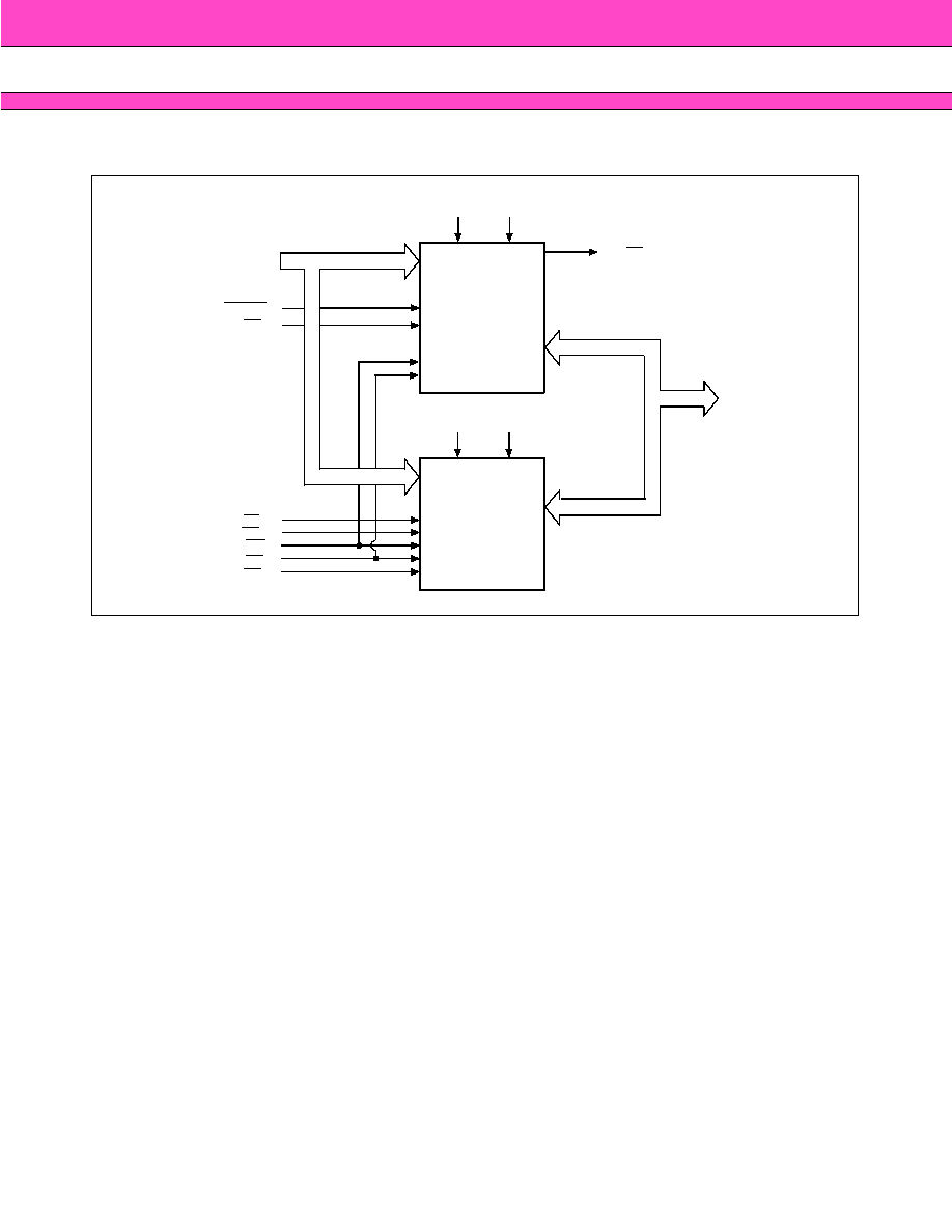
Table 1 Pin Configuration
Pin
Function
Input/
Output
A
0
to A
16
Address Inputs (Common)
I
A
17
to A
18
Address Input (Flash)
I
DQ
0
to DQ
15
Data Inputs/Outputs (Common)
I/O
CEf
Chip Enable (Flash)
I
CEs
Chip Enable (SRAM)
I
OE
Output Enable (Common)
I
WE
Write Enable (Common)
I
RY/BY
Ready/Busy Outputs (Flash)
O
UBs
Upper Byte Control (SRAM)
I
LBs
Lower Byte Control (SRAM)
I
RESET
Hardware Reset Pin/Sector Protection Unlock (Flash)
I
N.C.
No Internal Connection
--
V
SS
Device Ground (Common)
Power
V
CC
f
Device Power Supply (Flash)
Power
V
CC
s
Device Power Supply (SRAM)
Power

4
MB84VD2008
-10
/MB84VD2009
-10
s
PRODUCT LINE UP
s
BUS OPERATIONS
Legend: L = V
IL
, H = V
IH
, X = V
IL
or V
IH
. See DC Characteristics for voltage levels.
Notes: 1. Other operations except for indicated this column are inhibited.
2. WE can be V
IL
if OE is V
IL
, OE at V
IH
initiates the write operations.
3. Do not apply CEf = V
IL
, CEs = V
IL
at a time.
Flash Memory
SRAM
Ordering Part No.
V
CC
= 3.0 V
MB84VD2008-10/MB84VD2009-10
Max. Address Access Time (ns)
100
85
Max. CE Access Time (ns)
100
85
Max. OE Access Time (ns)
40
45
Table 2 User Bus Operations
Operation (1), (3)
CEf
CEs
OE
WE
LBs
UBs
DQ
0
to DQ
7
DQ
8
to DQ
15
RESET
Full Standby
H
H
X
X
X
X
HIGH-Z
HIGH-Z
H
Output Disable
H
L
H
H
X
X
HIGH-Z
HIGH-Z
H
X
X
H
H
HIGH-Z
HIGH-Z
L
H
H
H
X
X
HIGH-Z
HIGH-Z
Read from Flash (2)
L
H
L
H
X
X
D
OUT
D
OUT
H
Write to Flash
L
H
H
L
X
X
D
IN
D
IN
H
Read from SRAM
H
L
L
H
L
L
D
OUT
D
OUT
H
H
L
HIGH-Z
D
OUT
L
H
D
OUT
HIGH-Z
Write to SRAM
H
L
X
L
L
L
D
IN
D
IN
H
H
L
HIGH-Z
D
IN
L
H
D
IN
HIGH-Z
Flash Hardware Reset
X
H
X
X
X
X
HIGH-Z
HIGH-Z
L
+0.6 V
Ł0.3 V

5
MB84VD2008
-10
/MB84VD2009
-10
s
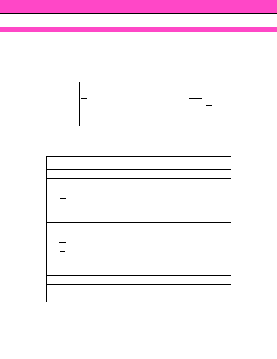
FLEXIBLE SECTOR-ERASE ARCHITECTURE on FLASH MEMORY
Ę Two 16 K byte, four 8 K bytes, two 32 K byte, and fourteen 64 K bytes.
Ę Individual-sector, multiple-sector, or bulk-erase capability.
16K byte/8K word
32K byte/16K word
8K byte/4K word
8K byte/4K word
8K byte/4K word
8K byte/4K word
32K byte/16K word
16K byte/8K word
64K byte/32K word
64K byte/32K word
64K byte/32K word
64K byte/32K word
64K byte/32K word
64K byte/32K word
64K byte/32K word
64K byte/32K word
64K byte/32K word
64K byte/32K word
64K byte/32K word
64K byte/32K word
64K byte/32K word
64K byte/32K word
7FFFFH
7E000H
7A000H
79000H
78000H
77000H
76000H
72000H
70000H
68000H
60000H
58000H
50000H
48000H
40000H
38000H
30000H
28000H
20000H
18000H
10000H
08000H
00000H
FFFFFH
FC000H
F4000H
F2000H
F0000H
EE000H
EC000H
E4000H
E0000H
D0000H
C0000H
B0000H
A0000H
90000H
80000H
70000H
60000H
50000H
40000H
30000H
20000H
10000H
00000H
64K byte/32K word
64K byte/32K word
64K byte/32K word
64K byte/32K word
64K byte/32K word
64K byte/32K word
64K byte/32K word
64K byte/32K word
64K byte/32K word
64K byte/32K word
64K byte/32K word
64K byte/32K word
64K byte/32K word
64K byte/32K word
16K byte/8K word
32K byte/16K word
8K byte/4K word
8K byte/4K word
8K byte/4K word
8K byte/4K word
32K byte/16K word
16K byte/8K word
FFFFFH
F0000H
E0000H
D0000H
C0000H
B0000H
A0000H
90000H
80000H
70000H
60000H
50000H
40000H
30000H
20000H
1C000H
14000H
12000H
10000H
0E000H
0C000H
04000H
00000H
7FFFFH
78000H
70000H
68000H
60000H
58000H
50000H
48000H
40000H
38000H
30000H
28000H
20000H
18000H
10000H
0C000H
0A000H
09000H
08000H
07000H
06000H
02000H
00000H
MBM29DL800TA Sector Architecture
MBM29DL800BA Sector Architecture
(
ū
16)
(
ū
8)
(
ū
16)
(
ū
8)
Bank 2
Bank 1
Bank 2
Bank 1
MB84VD2008 Sector Architecture
MB84VD2009 Sector Architecture