
DS05-11403-2E
FUJITSU SEMICONDUCTOR
DATA SHEET
MEMORY
CMOS
2
×
×
×
×
512 K
×
×
×
×
16 BIT
SINGLE DATA RATE I/F FCRAM
TM
Consumer
/
Embedded Application Specific Memory
MB81E161622-10/-12
CMOS 2-Bank
×
×
×
×
524,288-Word
×
×
×
×
16 Bit
Fast Cycle Random Access Memory (FCRAM) with Single Data Rate
s
s
s
s
DESCRIPTION
The Fujitsu MB81E161622 is a Fast Cycle Random Access Memory (FCRAM*) containing 16,777,216 memory
cells accessible in a 16-bit format. The MB81E161622 features a fully synchronous operation referenced to a
positive edge clock, whereby all operations are synchronized at a clock input which enables high performance
and simple user interface coexistence.
The MB81E161622 is utilized using a Fujitsu advanced FCRAM core technology and designed to improve the
random access performance and the complexity of controlling regular synchronous DRAM (SDRAM) which require
many wait state due to long latency constraints.
The MB81E161622 is ideally suited for various embedded/consumer applications including digital AVs, printers
and file storage where a large band width memory is needed.
* : FCRAM is a trademark of Fujitsu Limited, Japan.
s
s
s
s
PRODUCT LINEUP
Parameter
MB81E161622
-10
-12
Clock Frequency @CL
=
2
100 MHz Max
84 MHz Max
Burst Mode Cycle Time
CL
=
1
15 ns Min
20 ns Min
CL
=
2
10 ns Min
12 ns Min
Access Time From Clock
CL
=
1
10 ns Max
14 ns Max
CL
=
2
6 ns Max
7 ns Max
RAS Cycle Time
30 ns Min
36 ns Min
Operating Current (I
CC1
)
130 mA Max
120 mA Max
Power Down Mode Current (I
CC2P
)
0.6 mA Max
Self-refresh Current (I
CC6
)
0.6 mA Max

MB81E161622
-10/-12
2
s
s
s
s
FEATURES
s
s
s
s
PACKAGE
· Single
+
3.3 V Supply
±
0.3 V tolerance
· LVTTL compatible I/O interface
· Two-bank operation
· Programmable burst type, burst length, and
CAS latency
· 4 K refresh cycles every 64 ms
· Auto- and Self-refresh
· CKE power down mode
· Output Enable and Input Data Mask
54-pin Plastic TSOP (II) Package
(FPT-54P-M02)
(Normal Bend)
Marking side

MB81E161622
-10/-12
3
s
s
s
s
PIN ASSIGNMENT
s
PIN DESCRIPTIONS
*: These pins are connected internally in the chip.
Symbol
Function
V
CC
, V
CCQ
Supply Voltage
V
SS
, V
SSQ
*
Ground
DQ
0
to DQ
15
Data I/O
· Lower Byte : DQ
0
to DQ
7
· Upper Byte : DQ
8
to DQ
15
DQML, DQMU
DQ MASK
WE
Write Enable
CAS
Column Address Strobe
RAS
Row Address Strobe
CS
Chip Select
BA
Bank Select
AP
Auto Precharge Enable
A
0
to A
10
Address Input
· Row : A
0
to A
10
· Column : A
0
to A
7
CKE
Clock Enable
CLK
Clock Input
NC
No Connection
54-Pin TSOP (II)
(TOP VIEW)
<
Normal Bend : FPT-54P-M02
>
(Marking side)
V
CC
DQ
0
V
CCQ
DQ
1
DQ
2
V
SSQ
DQ
3
DQ
4
V
CCQ
DQ
5
DQ
6
V
SSQ
DQ
7
V
CC
DQML
WE
CAS
RAS
CS
NC
BA
A
10
/AP
A
0
A
1
A
2
A
3
V
CC
1
2
3
4
5
6
7
8
9
10
11
12
13
14
15
16
17
18
19
20
21
22
23
24
25
26
27
54
53
52
51
50
49
48
47
46
45
44
43
42
41
40
39
38
37
36
35
34
33
32
31
30
29
28
V
SS
DQ
15
V
SSQ
DQ
14
DQ
13
V
CCQ
DQ
12
DQ
11
V
SSQ
DQ
10
DQ
9
V
CCQ
DQ
8
V
SS
NC
DQMU
CLK
CKE
NC
NC
A
9
A
8
A
7
A
6
A
5
A
4
V
SS
MB81E161622
-10/-12
4
s
s
s
s
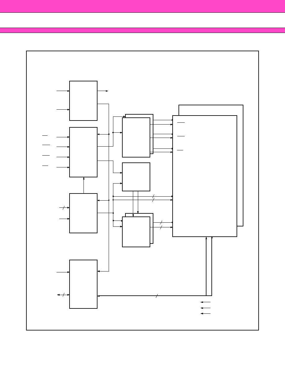
BLOCK DIAGRAM
CKE
CLK
CS
RAS
CAS
WE
RAS
CAS
WE
DQML,
DQMU
DQ
0
to
DQ
15
A
0
to A
9
,
A
10
/AP
BA
I/O
V
CC
V
SS
/V
SSQ
V
CCQ
16
11
8
CLOCK
BUFFER
COMMAND
DECODER
ADDRESS
BUFFER/
REGISTER
&
BANK SELECT
I/O DATA
BUFFER/
REGISTER
To each block
CONTROL
SIGNAL
LATCH
MODE
REGISTER
COLUMN
ADDRESS
COUNTER
DRAM
CORE
(2,048
×
256
×
16)
BANK-1
BANK-0
COL.
ADDR.
ROW
ADDR.
Fig. 1
-
-
-
-
MB81E161622 BLOCK DIAGRAM

MB81E161622
-10/-12
5
s
s
s
s
FUNCTIONAL TRUTH TABLE *
1
·
·
·
·
COMMAND TRUTH TABLE *
2,
*
3,
*
4
*1: V
=
Valid, L
=
Logic Low, H
=
Logic High, X
=
either L or H.
*2: All commands assumes no CSUS command on previous rising edge of clock.
*3: All commands are assumed to be valid state transitions.
*4: All inputs are latched on the rising edge of the clock.
*5: The NOP and DESL commands have the same effect on the part. Unless specifically noted, NOP will represent
both NOP and DESL commands in later descriptions.
*6: The READ, READA, WRIT and WRITA commands should be issued only after the corresponding bank has been
activated (ACTV command) . Refer to "STATE DIAGRAM" in section "
s
FUNCTIONAL DESCRIPTION."
*7: The ACTV command should be issued only after the corresponding bank has been precharged (PRE or PALL
command) .
*8: Required after power up. Refer to "POWER-UP INITIALIZATION" in section "
s
FUNCTIONAL DESCRIPTION."
*9: The MRS command should be issued only after all banks have been precharged (PRE or PALL command) and
DQ is in High-Z. Refer to "STATE DIAGRAM" in section "
s
FUNCTIONAL DESCRIPTION."
Function
Com-
mand
CKE
CS
RAS CAS
WE
BA
A
10
(AP)
A
9
,
A
8
A
7
to
A
0
n-1
n
Device Deselect
*5
DESL
H
X
H
X
X
X
X
X
X
X
No Operation
*5
NOP
H
X
L
H
H
H
X
X
X
X
Burst Stop
BST
H
X
L
H
H
L
X
X
X
X
Read
*6
READ
H
X
L
H
L
H
V
L
X
V
Read with Auto-precharge
*6 READA
H
X
L
H
L
H
V
H
X
V
Write
*6
WRIT
H
X
L
H
L
L
V
L
X
V
Write with Auto-precharge
*6
WRITA
H
X
L
H
L
L
V
H
X
V
Bank Active
*7
ACTV
H
X
L
L
H
H
V
V
V
V
Precharge Single Bank
*8
PRE
H
X
L
L
H
L
V
L
X
X
Precharge All Banks
*8
PALL
H
X
L
L
H
L
X
H
X
X
Mode Register Set
*8, 9
MRS
H
X
L
L
L
L
X
X
V
V