
DS04-28318-2E
FUJITSU SEMICONDUCTOR
DATA SHEET
ASSP
CMOS
85 MSPS 3ch 10-bit
D/A Converter
MB40C950V
s
DESCRIPTION
The MB40C950V is a high-speed CMOS process-based D/A converter provided with the three-channel I/O for
RGB, allowing for independent control of the three channels.
s
FEATURES
Ę Resolution
: 10 bits
Ę Linearity error
:
▒
1.5 LSB (max)
Ę Differential linearity error
:
▒
1.0 LSB (max)
Ę Maximum conversion rate
: 85 MSPS (min)
Ę Supply voltage
: single +5 V
Ę Digital input voltage range
: TTL level
Ę Analog output voltage range : 2 Vp-p (0 to 2V: analog output for RL = 200
, R
REF
= 3.3 k
, V
RIN
= 2V)
: 1 Vp-p (0 to 1V: analog output for RL = 75
, R
REF
= 2.4 k
, V
RIN
= 2V)
Ę Dissipation power
: 240 mW (standard: analog output for RL = 200
, 2 Vp-p output)
: 310 mW (standard: analog output for RL = 75
, 1 Vp-p output)
Ę Additional capabilities
: Power saving function, independent 3-ch V
REF
Ę Package
: LQFP64, QFP64
s
PACKAGES
64-pin Plastic LQFP
(FPT-64P-M03)
64-pin Plastic QFP
(FPT-64P-M10)

4
MB40C950V
s
PIN DESCRIPTION
Pin No.
Symbol
I/O
Description
LQFP64
QFP64
4 to 13
15 to 24
29 to 38
5 to 14
18 to 27
29 to 38
R
0
to R
9
G
0
to G
9
B
0
to B
9
I
Data signal incoming terminal for Rch, Gch and Bch
LSB: R
0
, G
0
, B
0
MSB: R
9
, G
9
,B
9
42
43
44
45
46
47
RCLK
GCLK
BCLK
I
Clock signal incoming terminal for Rch, Gch and Bch
61
62
CE
I
Power saving signal incoming terminal. Power saving
enabled for High
62
63
DV
DD
--
Digital power supply terminal
54, 60
55, 61
AV
DD
--
Analog power supply terminal
40
43
DV
SS
--
Digital ground terminal
56, 58
57, 59
AV
SS
--
Analog ground terminal
63
51
48
64
52
50
RV
RIN
GV
RIN
BV
RIN
I
Rererence voltage incoming terminal for Rch, Gch and
Bch
64
53
49
1
54
51
RI
REF
GI
REF
BI
REF
--
Reference resistor connection terminal for Rch, Gch and
Bch
41
44
VA
--
Connect >0.1
Ą
F capacitor to the AV
SS
terminal
1
52
47
2
53
49
RV
B
GV
B
BV
B
--
Connect >0.1
Ą
F capacitor to the AV
DD
terminal
59
57
55
60
58
56
R
OUT
G
OUT
B
OUT
O
Analog signal output terminals for Rch, Gch and Bch
2 to 3
14
25 to 28
39, 45
46, 50
3 to 4
15 to 17
28
39 to 42
48
N.C.
--
Not connected. To be left open.
5
MB40C950V
s
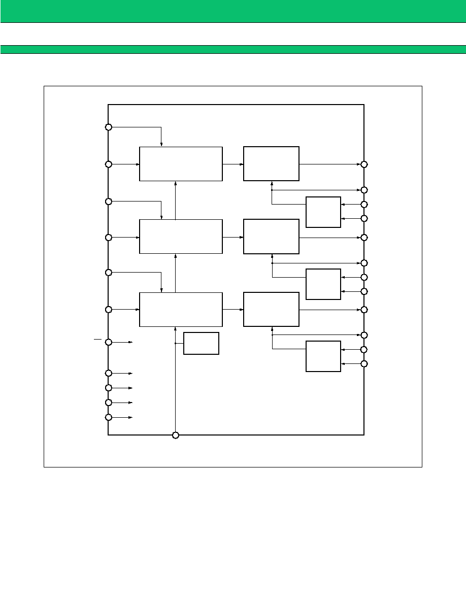
BLOCK DIAGRAM
RCLK
Decorder and latch circuit
Decorder and latch circuit
Decorder and latch circuit
REF circuit
Reference
current
generator
circuit
GCLK
BCLK
AV
DD
DV
DD
AV
SS
DV
SS
CE
R
0
to R
9
G
0
to G
9
B
0
to B
9
VA
R
OUT
RV
B
RV
RIN
RI
REF
G
OUT
B
OUT
GV
B
GV
RIN
GI
REF
BV
B
BV
RIN
BI
REF
Current cell
Current cell
Current cell
Reference
current
generator
circuit
Reference
current
generator
circuit

