1
DS04-21360-4E
FUJITSU SEMICONDUCTOR
DATA SHEET
ASSP
Single Serial Input
PLL Frequency Synthesizer
On-chip 2.0 GHz Prescaler
MB15E05SL
s
DESCRIPTION
The Fujitsu MB15E05SL is a serial input Phase Locked Loop (PLL) frequency synthesizer with a 2.0 GHz prescaler.
The 2.0 GHz prescaler has a dual modulus division ratio of 64/65 or 128/129 enabling pulse swallowing operation.
The supply voltage range is between 2.4 V and 3.6 V. The MB15E05SL uses the latest BiCMOS process, as a result
the supply current is typically 3.0 mA at 2.7 V. A refined charge pump supplies well-balanced output currents of 1.5
mA and 6 mA. The charge pump current is selectable by serial data.
MB15E05SL is ideally suited for wireless mobile communications, such as GSM (Global System for Mobile
Communications) and PCS.
s
FEATURES
· High frequency operation: 2.0 GHz max
· Low power supply voltage: V
CC
= 2.4 to 3.6 V
· Ultra Low power supply current: I
CC
= 3.0 mA typ. (V
CC
= Vp = 2.7 V, Ta = +25
°
C, in locking state)
I
CC
= 3.5 mA typ. (V
CC
= Vp = 3.0 V, Ta = +25
°
C, in locking state)
· Direct power saving function: Power supply current in power saving mode
Typ. 0.1
µ
A (V
CC
= Vp = 3.0 V, Ta = +25
°
C), Max. 10
µ
A (V
CC
= Vp = 3.0 V)
· Dual modulus prescaler: 64/65 or 128/129
· Serial input 14-bit programmable reference divider: R = 3 to 16,383
· Serial input programmable divider consisting of:
- Binary 7-bit swallow counter: 0 to 127
- Binary 11-bit programmable counter: 3 to 2,047
· Software selectable charge pump current
· On-chip phase control for phase comparator
· Operating temperature: Ta = 40 to +85
°
C
· Pin compatible with MB15E05, MB15E05L
s
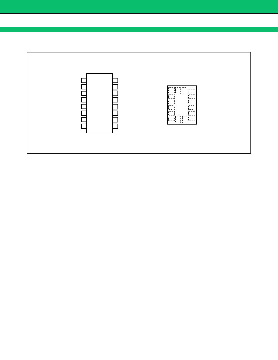
PACKAGES
16-pin plastic SSOP
(FPT-16P-M05)
16-pad plastic BCC
(LCC-16P-M06)
3
MB15E05SL
s
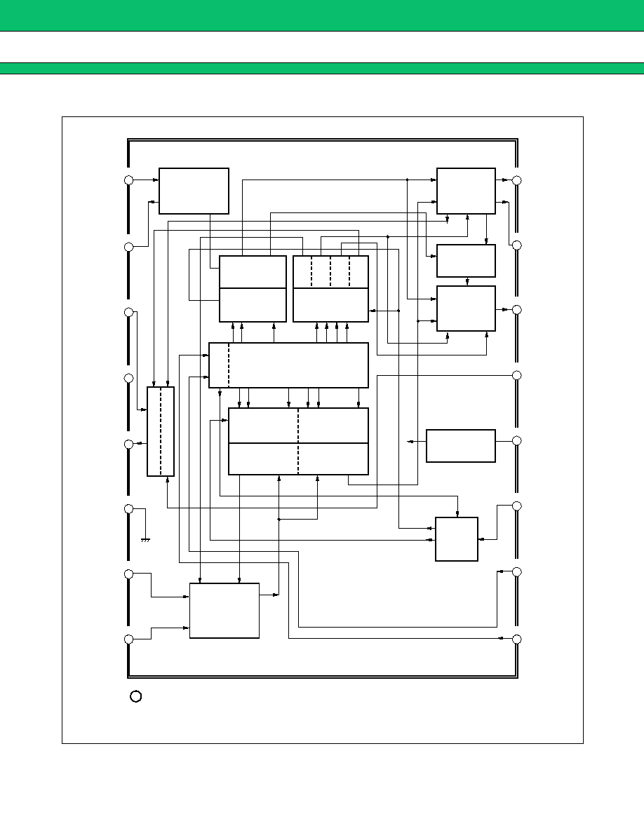
PIN DESCRIPTIONS
Pin no.
Pin
name
I/O
Descriptions
SSOP
BCC
1
16
OSC
IN
I
Programmable reference divider input. Connection to a TCXO.
2
1
OSC
OUT
O
Oscillator output.
3
2
V
P
Power supply voltage input for the charge pump.
4
3
V
CC
Power supply voltage input.
5
4
D
O
O
Charge pump output.
Phase of the charge pump can be selected via programming of the FC bit.
6
5
GND
Ground.
7
6
Xfin
I
Prescaler complementary input, which should be grounded via a capacitor.
8
7
fin
I
Prescaler input.
Connection to an external VCO should be done via AC coupling.
9
8
Clock
I
Clock input for the 19-bit shift register.
Data is shifted into the shift register on the rising edge of the clock.
(Open is prohibited.)
10
9
Data
I
Serial data input using binary code.
The last bit of the data is a control bit. (Open is prohibited.)
11
10
LE
I
Load enable signal input. (Open is prohibited.)
When LE is set high, the data in the shift register is transferred to a latch
according to the control bit in the serial data.
12
11
PS
I
Power saving mode control. This pin must be set at "L" at Power-ON.
(Open is prohibited.)
PS = "H"; Normal mode
PS = "L"; Power saving mode
13
12
ZC
I
Forced high-impedance control for the charge pump (with internal pull up
resistor.)
ZC = "H"; Normal Do output.
ZC = "L"; Do becomes high impedance.
14
13
LD/fout
O
Lock detect signal output (LD)/phase comparator monitoring output (fout).
The output signal is selected via programming of the LDS bit.
LDS = "H"; outputs fout (fr/fp monitoring output)
LDS = "L"; outputs LD ("H" at locking, "L" at unlocking.)
15
14
P
O
Phase comparator N-channel open drain output for an external charge
pump. Phase can be selected via programming of the FC bit.
16
15
R
O
Phase comparator CMOS output for an external charge pump. Phase can
be selected via programming of the FC bit.
5
MB15E05SL
s
ABSOLUTE MAXIMUM RATINGS
WARNING: Semiconductor devices can be permanently damaged by application of stress (voltage, current,
temperature, etc.) in excess of absolute maximum ratings. Do not exceed these ratings.
s
RECOMMENDED OPERATING CONDITIONS
WARNING: The recommended operating conditions are required in order to ensure the normal operation of the
semiconductor device. All of the device's electrical characteristics are warranted when the device is
operated within these ranges.
Always use semiconductor devices within their recommended operating condition ranges. Operation
outside these ranges may adversely affect reliability and could result in device failure.
No warranty is made with respect to uses, operating conditions, or combinations not represented on
the data sheet. Users considering application outside the listed conditions are advised to contact their
FUJITSU representatives beforehand.
Parameter
Symbol
Condition
Rating
Unit
Remark
Min.
Max.
Power supply voltage
V
CC
0.5
4.0
V
V
P
V
CC
6.0
V
Input voltage
V
I
0.5
V
CC
+0.5
V
Output voltage
V
O
Except Do
GND
V
CC
V
V
O
Do
GND
V
P
V
Storage temperature
Tstg
55
+125
°
C
Parameter
Symbol
Value
Unit
Remark
Min.
Typ.
Max.
Power supply voltage
V
CC
2.4
3.0
3.6
V
V
P
V
CC
5.5
V
Input voltage
V
I
GND
V
CC
V
Operating temperature
Ta
40
+85
°
C