
DS06-80106-2E
FUJITSU SEMICONDUCTOR
DATA SHEET
SEMICUSTOM
Built-in IF Band Voltage Controlled Oscillator
Mask ROM Frequency Synthesizer
MB15C700 series
s
s
s
s
DESCRIPTION
MB15C700 series is a Phase Locked Loop (PLL) frequency synthesizer of pulse swallow operation with built-in
VCO suitable for Intermediate Frequency band synthesizer of mobile phones.
The VCO can operate option oscillation frequency by an external inductance and capacitor. The PLL reference
divider ratio and comparison divider ratio are fixed , so that it is not required to set the divider ratios by a
microcontroller externally. BCC-20 plastic package is miniaturized the device and makes it easier to design.
It operates with a supply voltage of 2.5 V typ. (PLLVDD, VCOVDD) and low power consumption current 4.5 mA
typ. (PLL
+
VCO at 400 MHz) is realized by pure- CMOS technology.
s
s
s
s
FEATURES
<<PLL>>
· Pulse swallow function
· 400 MHz High-speed Prescaler : 8/9, 16/17, 32/33
· MASK ROM optinal the comparison and reference dividers :
Comparison counter : Main counter : 5 to 4095, Swallow counter : 0 to 31
Reference counter : 5 to 4095 (up to 26 MH
Z
)
· Lock detector circuit: Digital lock detector circuit which is
"
H
"
level when PLL is locked.
(Continued)
s
s
s
s
PACKAGE
20-pad, plastic BCC
LCC-20P-M04

MB15C700 series
2
(Continued)
· Charge pump options :
H type: Super charger circuit for high speed tuning. (I
OH
=
-
4.5 mA, I
OL
= 4.5 mA at PLLVDD = 2.5 V)
L type : Low sensitivity charge pump for direct modulation. (I
OH
=
-
1.125 mA, I
OL
= 1.125 mA at PLLVDD = 2.5 V)
<<VCO>>
· Integrates vari-cap for VCO
· Operating frequency can be arranged by the number of the external inductor and capacitor connected TANK
circuit
<<COMMON>>
· Low power supply voltage : 2.3 V to 2.7 V
· Low power supply current : 4.5 mA typ. (PLLVDD
=
VCOVDD
=
2.5 V, fvco
=
400 MHz)
· Operating temperature :
-
20
°
C to
+
85
°
C
s
s
s
s
PIN ASSIGNMENT
1
2
3
4
5
6
7
8
9
10
11
12
13
14
15
16
17
18
19
20
VCOGND
N.C.
VCOCNT
VCOPS
VCOVDD
LD
VCOTNKO
VCOTNKI
N.C.
N.C.
OSCin
PLLVDD
fout
VCOout
PLLPS
PLLfin
PLLGND
PLLDo
N.C.
N.C.
LCC-20P-M04
(Top View)

MB15C700 series
3
s
s
s
s
PIN DESCRIPTIONS
Pin
No.
Symbol
I/O
Descriptions
1
VCOGND
Ground for the VCO.
2
N.C.
No connection.
3
VCOCNT
I
VCO control voltage input.
Connection to PLLDo terminal via LPF.
4
VCOPS
I
Power saving control for the VCO. (Open is prohibited.)
"H" : Normal mode
"L" : Power saving mode
5
VCOVDD
Power supply voltage input for VCO.
Connect to capacitor between GND.
6
LD
O
Lock detector signal output.
LD
=
"H" : Locking mode or power saving mode
LD
=
"L" : Unlocking mode.
7
N.C.
No connection.
8
OSCin
I
The reference counter input.
Connect with a AC coupling capacitor.
9
fout
O
Test purpose output. This pin is an open drain output.
10
PLLVDD
Power supply voltage input for the PLL.
Connect to capacitor between GND
11
N.C.
No connection
12
N.C.
No connection.
13
PLLDo
O
PLL charge pump output.
Connect to VCOCNT pin via LPF.
14
PLLGND
Ground for the PLL.
15
PLLfin
I
Prescaler input.
Connect with an AC coupling capacitor.
16
PLLPS
I
Power saving control for the PLL. (Open is prohibited.)
"H": Normal mode
"L": Power saving mode
17
N.C.
No connection.
18
VCOout
O
VCO output.
19
VCOTNKI
I
VCOTANK circuit input.
Connect to VCOTNKO pin with inductance and resistance.
Connect to capacitor between GND.
20
VCOTNKO
O
VCOTANK circuit output.
Connect to VCOTNKI terminal with inductance and resistance.
Connect to capacitor between GND. (max.2.0 pF)
MB15C700 series
4
s
s
s
s
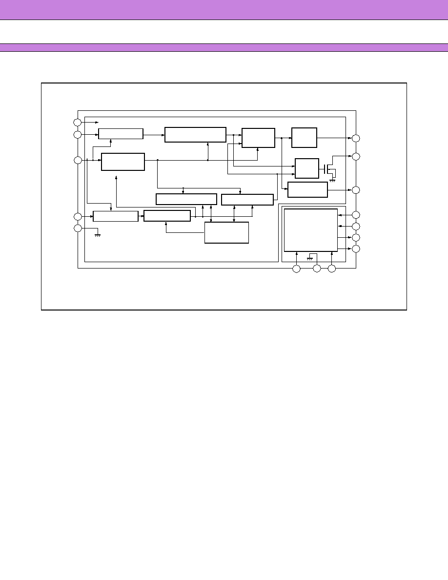
BLOCK DIAGRAM
s
s
s
s
FUNCTIONAL DESCRIPTIONS
Divide ratios of the internal counters can be set optionally according to customer requirements.
The divide ratio can be calculated using the following equation.
fvco
=
[ (P
×
N
+
A) ]
×
fosc
/
R
Note: N
>
A, P
>
A
fvco
: Output frequency of Voltage Controlled Oscillator (VCOout up to 400 MHz)
fosc
: Reference oscillation frequency (up to 26 MHz)
N
: Divide ratio of the main counter (5 to 4095)
A
: Divide ratio of the swallow counter (0 to 31)
P
: Preset divide ratio of dual modulus prescaler (8/9, 16/17, 32/33)
R
: Divide ratio of the reference counter (5 to 4095)
LD
fout
PLLDo
VCOCNT
VCOTNKI
VCOTNKO
VCOout
VCOVDD
VCOGND
VCOPS
PLLVDD
OSCin
PLLPS
PLLfin
PLLGND
PLL-Block
VCO-Block
10
6
14
15
16
8
9
13
19
3
18
20
14
4
5
Buffer Amp.
Buffer Amp.
Power saving
control circuit
Reference counter (R)
Phase
comparator
Lock
detector
Output
selector
Charge pump
Prescaler (P)
Swallow counter (A)
Main counter (N)
Control
circuit
MB15C700 series
5
s
s
s
s
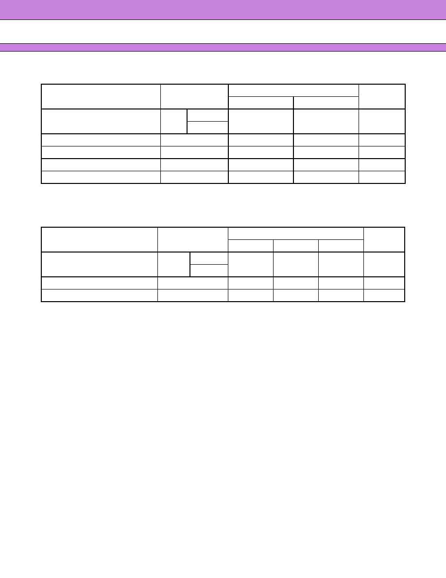
ABSOLUTE MAXIMUM RATINGS
WARNING: Semiconductor devices can be permanently damaged by application of stress (voltage, current,
temperature, etc.) in excess of absolute maximum ratings. Do not exceed these ratings.
s
s
s
s
RECOMMENDED OPERATING CONDITIONS
WARNING: The recommended operating conditions are required in order to ensure the normal operation of the
semiconductor device. All of the device's electrical characteristics are warranted when the device is
operated within these ranges.
Always use semiconductor devices within their recommended operating condition ranges. Operation
outside these ranges may adversely affect reliability and could result in device failure.
No warranty is made with respect to uses, operating conditions, or combinations not represented on
the data sheet. Users considering application outside the listed conditions are advised to contact their
FUJITSU representatives beforehand.
Parameter
Symbol
Rating
Unit
Min.
Max.
Power supply voltage
V
DD
PLLVDD
-
0.5
4.0
V
VCOVDD
Output voltage
V
O
-
0.5
V
DD
+
0.5
V
Input voltage
V
I
-
0.5
V
DD
+
0.5
V
Output current
I
O
0
+
5.0
mA
Storage temperature
T
stg
-
55
+
125
°
C
Parameter
Symbol
Value
Unit
Min.
Typ.
Max.
Power supply voltage
V
DD
PLLVDD
2.3
2.5
2.7
V
VCOVDD
Input voltage
V
IN
GND
V
DD
V
Operating temperature
Ta
-
20
+
85
°
C