Äîêóìåíòàöèÿ è îïèñàíèÿ www.docs.chipfind.ru
© 2005 Fairchild Semiconductor Corporation
DS500387
www.fairchildsemi.com
September 2000
Revised June 2005
SSTV168
57
· SSTVN16857 14-Bi
t Regist
er wit
h
SSTL-
2 C
o
m
p
ati
b
l
e
I
/
O and
Rese
t
SSTV16857 · SSTVN16857
14-Bit Register with SSTL-2 Compatible I/O and Reset
General Description
The SSTV16857 is a 14-bit register designed for use with
184 and 232 pin PC1600, 2100, and 2700 DDR DIMM
applications. The SSTVN16857 is a 14-bit register
designed for use with 184 and 232 pin PC3200 DDR DIMM
applications. These devices have a differential input clock,
SSTL-2 compatible data inputs and a LVCMOS compatible
RESET input. These devices have been designed for com-
pliance with the JEDEC DDR module and register specifi-
cations.
The devices are fabricated on an advanced submicron
CMOS process and are designed to operate at power sup-
plies of less than 3.6V's.
Features
s
Compliant with DDR-I registered module specifications
s
Operates at 2.5V
r
0.2V V
DD
s
SSTL-2 compatible input and output structure
s
Differential SSTL-2 compatible clock inputs
s
Low power mode when device is reset
s
Industry standard 48 pin TSSOP package
Ordering Code:
Devices also available in Tape and Reel. Specify by appending the suffix letter "X" to the ordering code.
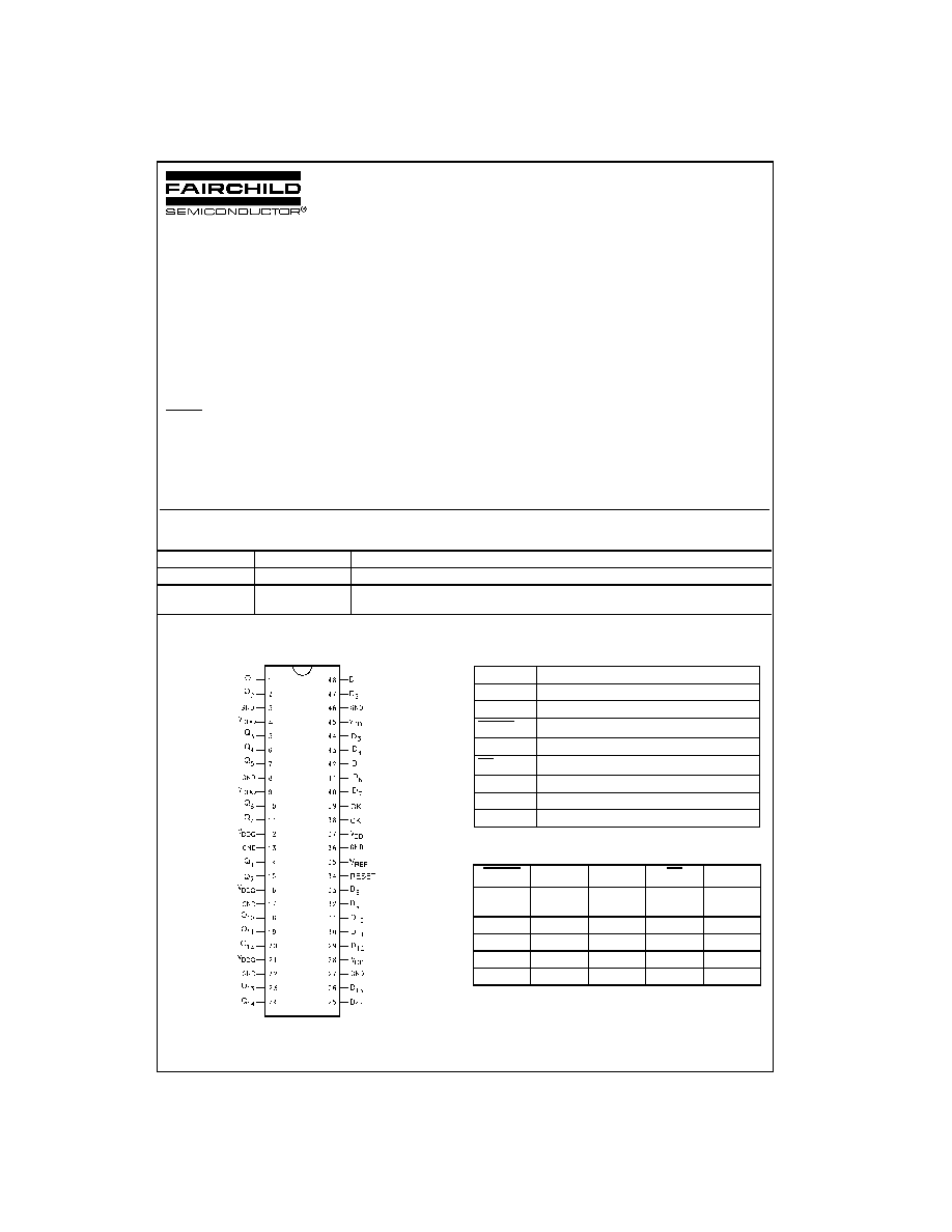
Connection Diagram
Pin Descriptions
Truth Table
L
Logic LOW
H
Logic HIGH
X
Don't Care, but not floating unless noted
n
LOW-to-HIGH Clock Transition
p
HIGH-to-LOW Clock Transition
Order Number
Package Number
Package Description
SSTV16857MTD
MTD48
48-Lead Thin Shrink Small Outline Package (TSSOP), JEDEC MO-153, 6.1mm Wide
SSTVN16857MTD
(Preliminary)
MTD48
48-Lead Thin Shrink Small Outline Package (TSSOP), JEDEC MO-153, 6.1mm Wide
Pin Name
Description
Q
1
-Q
14
SSTL-2 Compatible Output
D
1
-D
14
SSTL-2 Compatible Inputs
RESET
Asynchronous LVCMOS Reset Input
CK
Positive Master Clock Input
CK
Negative Master Clock Input
V
REF
Voltage Reference Pin for SSTL Level Inputs
V
DDQ
Power Supply Voltage for Output Signals
V
DD
Power Supply Voltage for Inputs
RESET
D
n
CK
CK
Q
n
L
X or
Floating
X or
Floating
X or
Floating
L
H
L
n
p
L
H
H
n
p
H
H
X
L
H
Q
n
H
X
H
L
Q
n
www.fairchildsemi.com
2
SSTV16857
·
SSTVN16857
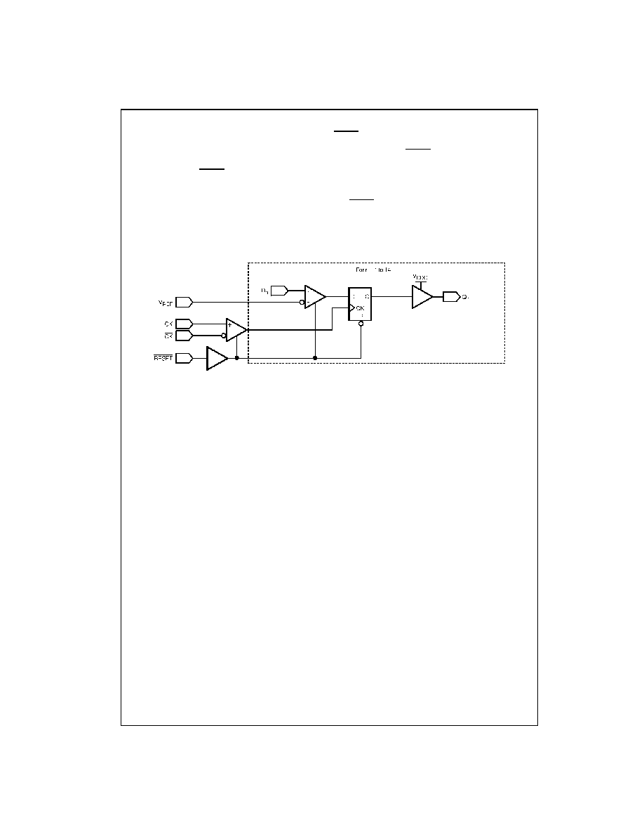
Functional Description
The SSTV16857 and SSTVN16587 are 14-bit registers
with SSTL-2 compatible inputs and outputs. Input data is
captured by the register on the positive edge crossing of
the differential clock pair.
When the LV-CMOS RESET signal is asserted LOW, all
outputs and internal registers are asynchronously placed
into the LOW logic state. In addition, the clock and data dif-
ferential comparators are disabled for power savings. Out-
put glitches are prevented by disabling the internal
registers more quickly than the input comparators. When
RESET is removed, the system designer must insure the
clock and data inputs to the device are stable during the
rising transition of the RESET signal.
The SSTL-2 data inputs transition based on the value of
V
REF
. V
REF
is a stable system reference used for setting
the trip point of the input buffers of the SSTV16857/
SSTVN16857 and other SSTL-2 compatible devices.
The RESET signal is a standard CMOS compatible input
and is not referenced to the V
REF
signal.
Logic Diagram
3
www.fairchildsemi.com
SSTV168
57
·
SSTVN16857
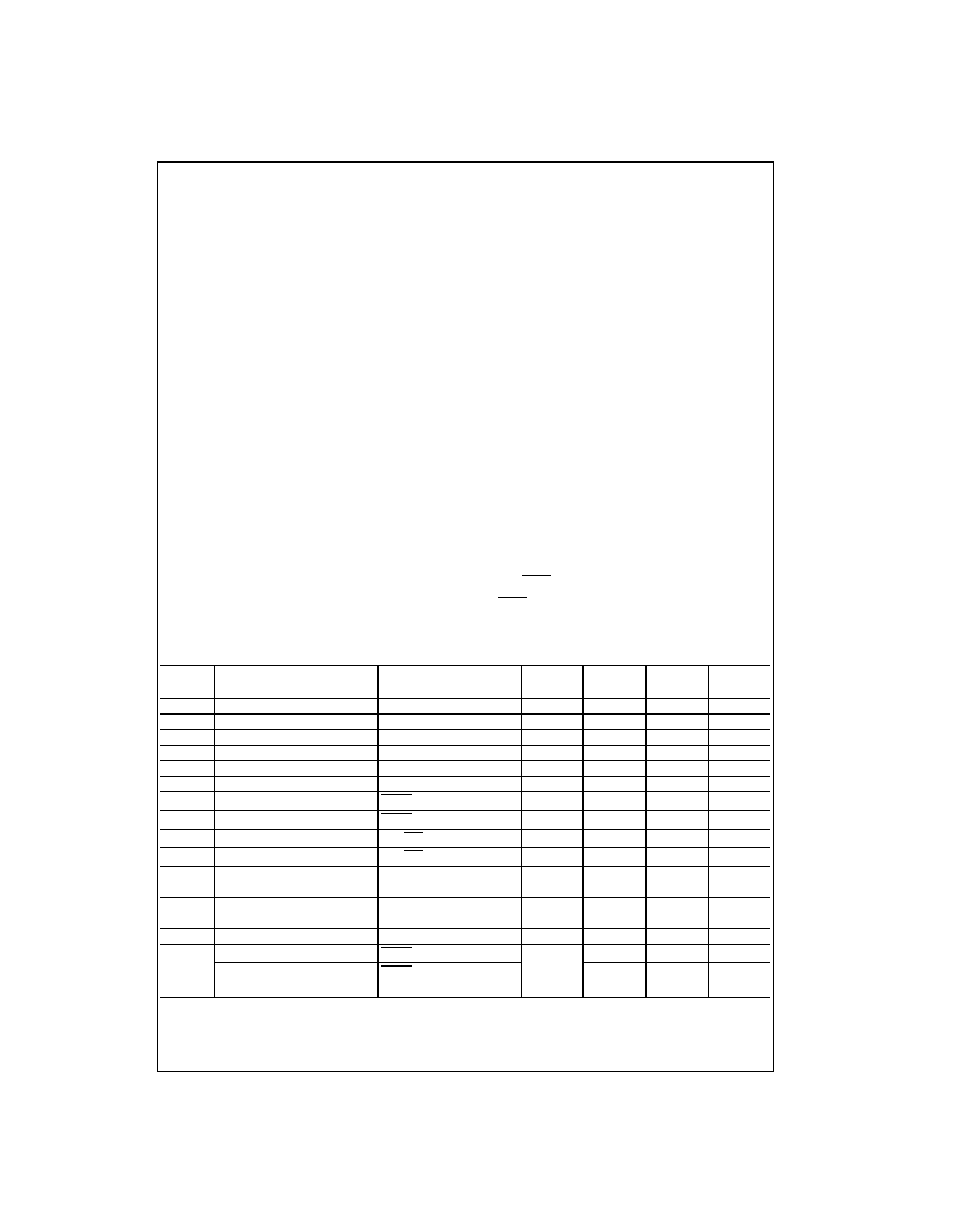
Absolute Maximum Ratings
(Note 1)
Recommended Operating
Conditions
(Note 3)
Note 1: The "Absolute Maximum Ratings" are those values beyond which
the safety of the device cannot be guaranteed. The device should not be
operated at these limits. The parametric values defined in the "Electrical
Characteristics" table are not guaranteed at the absolute maximum ratings.
The "Recommended Operating Conditions" table will define the conditions
for actual device operation.
Note 2: IO Absolute Maximum Rating must be observed.
Note 3: The RESET input of the device must be held at V
DD
or GND to
ensure proper device operation. The differential inputs must not be floating,
unless RESET is asserted LOW.
DC Electrical Characteristics (SSTV16857)
(2.3V
d
V
DD
d
2.7V)
Supply Voltage (V
DDQ
)
0.5V to
3.6V
Supply Voltage (V
DD
)
0.5V to
3.6V
Reference Voltage (V
REF
)
0.5V to
3.6V
Input Voltage (V
I
)
0.5V to V
DD
0.5V
Output Voltage (V
O
)
Outputs Active (Note 2)
0.5V to V
DDQ
0.5V
DC Input Diode Current (I
IK
)
V
I
0V
50 mA
V
I
!
V
DD
50 mA
DC Output Diode Current (I
OK
)
V
O
0V
50 mA
V
O
!
V
DD
50 mA
DC Output Source/Sink Current
(I
OH
/I
OL
)
r
50 mA
DC V
DD
or Ground Current
per Supply Pin (I
DD
or Ground)
r
100 mA
Storage Temperature Range (T
stg
)
65
q
C to
150
q
C
Power Supply (V
DDQ
)
SSTV16857
2.3V to 2.7V
SSTVN16857
2.5V to 2.7V
Power Supply (V
DD
)
Operating Range
V
DDQ
to 2.7V
Reference Supply (V
REF
V
DDQ
/2)
SSTV16857
1.15 to 1.35
SSTVN16857
1.25 to 1.35
Termination Voltage (V
TT
)
V
REF
r
40 mV
Input Voltage
0V to V
DD
Output Voltage (V
O
)
Output in Active States
0V to V
DDQ
Output Current I
OH
/I
OL
V
DD
2.3V to 2.7V
SSTV16857
r
20 mA
V
DD
2.5V to 2.7V
SSTVN16857
r
20 mA
Free Air Operating Temperature (T
A
)
0
q
C to
70
q
C
Symbol
Parameter
Conditions
V
DD
Min
Max
Units
(V)
V
IKL
Input LOW Clamp Voltage
I
I
18 mA
2.3
1.2
V
V
IKH
Input HIGH Clamp Voltage
I
I
18 mA
2.3
3.5
V
V
IH-AC
AC HIGH Level Input Voltage
Data Inputs
V
REF
310mV
V
V
IL-AC
AC LOW Level Input Voltage
Data Inputs
V
REF
310mV
V
V
IH-DC
DC HIGH Level Input Voltage
Data Inputs
V
REF
150mV
V
V
IL-DC
DC LOW Level Input Voltage
Data Inputs
V
REF
150mV
V
V
IH
HIGH Level Input Voltage
RESET
1.7
V
V
IL
LOW Level Input Voltage
RESET
0.7
V
V
ICR
Common Mode Input Voltage Range
CLK, CLK
0.97
1.53
V
V
I(PP)
Peak to Peak Input Voltage
CLK, CLK
360
mV
V
OH
HIGH Level Output Voltage
I
OH
100
P
A
2.3 to 2.7
V
DD
0.2
V
I
OH
16 mA
2.3
1.95
V
OL
LOW Level Output Voltage
I
OL
100
P
A
2.3 to 2.7
0.2
V
I
OL
16 mA
2.3
0.35
I
I
Input Leakage Current
V
I
V
DD
or GND
2.7
r
5.0
P
A
I
DD
Static Standby
RESET
GND, I
O
0
2.7
10
P
A
Static Operating
RESET
V
DD
, I
O
0
25
mA
V
I
V
IH(AC)
or V
IL(AC)
www.fairchildsemi.com
4
SSTV16857
·
SSTVN16857
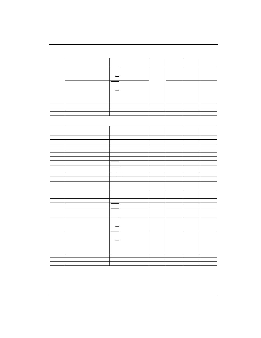
DC Electrical Characteristics (SSTV16857)
(Continued)
DC Electrical Characteristics (SSTVN16857)
(2.5V
d
V
DD
d
2.7V)
Symbol
Parameter
Conditions
V
DD
Min
Max
Units
(V)
I
DDD
Dynamic Operating Current
RESET
V
DD
, I
O
0
2.7
P
A/MHz
Clock Only
V
I
V
IH(AC)
or V
IL(AC)
90
CK, CK Duty Cycle 50%
Dynamic Operating Current
RESET
V
DD
, I
O
0
P
A/MHz
per Data Input
V
I
V
IH(AC)
or V
IL(AC)
CK, CK Duty Cycle 50%
15
Data Input
½ Clock
Rate 50% Duty Cycle
R
OH
Output HIGH On Resistance
I
OH
20 mA
2.3 to 2.7
7
20
:
R
OL
Output LOW On Resistance
I
OL
20 mA
2.3 to 2.7
7
20
:
R
O
'
| R
OH
- R
OL
|
I
O
20 mA, T
A
25
q
C
2.5
4
:
Symbol
Parameter
Conditions
V
DD
Min
Max
Units
(V)
V
IKL
Input LOW Clamp Voltage
I
I
18 mA
2.5
1.2
V
V
IKH
Input HIGH Clamp Voltage
I
I
18 mA
2.5
3.5
V
V
IH-AC
AC HIGH Level Input Voltage
Data Inputs
V
REF
310mV
V
V
IL-AC
AC LOW Level Input Voltage
Data Inputs
V
REF
310mV
V
V
IH-DC
DC HIGH Level Input Voltage
Data Inputs
V
REF
150mV
V
V
IL-DC
DC LOW Level Input Voltage
Data Inputs
V
REF
150mV
V
V
IH
HIGH Level Input Voltage
RESET
1.7
V
V
IL
LOW Level Input Voltage
RESET
0.7
V
V
ICR
Common Mode Input Voltage Range
CLK, CLK
0.97
1.53
V
V
I(PP)
Peak to Peak Input Voltage
CLK, CLK
360
mV
V
OH
HIGH Level Output Voltage
I
OH
100
P
A
2.5 to 2.7
V
DD
0.2
V
I
OH
16 mA
2.5
1.95
V
OL
LOW Level Output Voltage
I
OL
100
P
A
2.5 to 2.7
0.2
V
I
OL
16 mA
2.5
0.35
I
I
Input Leakage Current
V
I
V
DD
or GND
2.7
r
5.0
P
A
I
DD
Static Standby
RESET
GND, I
O
0
2.7
10
P
A
Static Operating
RESET
V
DD
, I
O
0
25
mA
V
I
V
IH(AC)
or V
IL(AC)
I
DDD
Dynamic Operating Current
RESET
V
DD
, I
O
0
2.7
P
A/MHz
Clock Only
V
I
V
IH(AC)
or V
IL(AC)
90
CK, CK Duty Cycle 50%
Dynamic Operating Current
RESET
V
DD
, I
O
0
P
A/MHz
per Data Input
V
I
V
IH(AC)
or V
IL(AC)
CK, CK Duty Cycle 50%
15
Data Input
½ Clock
Rate 50% Duty Cycle
R
OH
Output HIGH On Resistance
I
OH
20 mA
2.5 to 2.7
7
20
:
R
OL
Output LOW On Resistance
I
OL
20 mA
2.5 to 2.7
7
20
:
R
O
'
| R
OH
- R
OL
|
I
O
20 mA, T
A
25
q
C
2.5
4
:
5
www.fairchildsemi.com
SSTV168
57
·
SSTVN16857
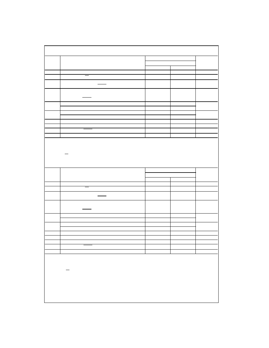
AC Electrical Characteristics (SSTV16857)
(Note 4)
Note 4: Refer to Figure 1 through Figure 7.
Note 5: This parameter is not production tested.
Note 6: For data signal input slew rate
t
1 V/ns.
Note 7: For data signal input slew rate
t
0.5 V/ns and
1 V/ns.
Note 8: For CK, CK signals input slew rates are
t
1 V/ns.
AC Electrical Characteristics (SSTVN16857)
(Note 9)
Note 9: Refer to Figure 1 through Figure 7.
Note 10: This parameter is not production tested.
Note 11: For data signal input slew rate
t
1 V/ns.
Note 12: For data signal input slew rate
t
0.5 V/ns and
1 V/ns.
Note 13: For CK, CK signals input slew rates are
t
1 V/ns.
Note 14: Simultaneous Switching is guaranteed by characterization.
Symbol
Parameter
T
A
0
q
C to
70
q
C, C
L
30 pF, R
L
50
:
Units
V
DD
2.5V
r
0.2V; V
DDQ
2.5V
r
0.2V
Min
Max
f
MAX
Maximum Clock Frequency
200
MHz
t
W
Pulse Duration, CK, CK HIGH or LOW (Figure 2)
2.5
ns
t
ACT
Differential Inputs Activation Time,
22
ns
(Note 5)
data inputs must be LOW after RESET HIGH (Figure 3)
t
INACT
Differential Inputs De-activation Time,
22
ns
(Note 5)
data and clock inputs must be held at valid levels
(not floating) after RESET LOW
t
S
Setup Time, Fast Slew Rate (Note 6)(Note 7) (Figure 5)
0.65
ns
Setup Time, Slow Slew Rate (Note 7)(Note 8) (Figure 5)
0.9
t
H
Hold Time, Fast Slew Rate (Note 6)(Note 8) (Figure 5)
0.75
ns
Hold Time, Slow Slew Rate (Note 7)(Note 8) (Figure 5)
0.9
t
REM
Reset Removal Time (Figure 7)
10
ns
t
PHL
, t
PLH
Propagation Delay CLK, CLK to Q
n
(Figure 4)
1.1
2.8
ns
t
PHL
Propagation Delay RESET to Q
n
(Figure 6)
5.0
ns
t
SK(Pn-Pn)
Output to Output Skew
200
ps
Symbol
Parameter
T
A
0
q
C to
70
q
C, C
L
30 pF, R
L
50
:
Units
V
DD
2.5V
r
0.2V; V
DDQ
2.5V
r
0.2V
Min
Max
f
MAX
Maximum Clock Frequency
220
MHz
t
W
Pulse Duration, CK, CK HIGH or LOW (Figure 2)
2.5
ns
t
ACT
Differential Inputs Activation Time,
22
ns
(Note 5)
data inputs must be LOW after RESET HIGH (Figure 3)
t
INACT
Differential Inputs De-activation Time,
22
ns
(Note 5)
Data and Clock Inputs must be held at valid levels
(not floating) after RESET LOW
t
S
Setup Time, Fast Slew Rate (Note 9)(Note 12) (Figure 5)
0.65
ns
Setup Time, Slow Slew Rate (Note 12)(Note 13) (Figure 5)
0.75
t
H
Hold Time, Fast Slew Rate (Note 11)(Note 13) (Figure 5)
0.75
ns
Hold Time, Slow Slew Rate (Note 12)(Note 13) (Figure 5)
0.9
t
REM
Reset Removal Time (Figure 7)
10
ns
t
PHL
, t
PLH
Propagation Delay CLK, CLK to Q
n
(Figure 4)
1.1
2.4
ns
t
PSS
Propagation Delay Simultaneous Switching CLK, CLK to Q
n
(Note 14)
2.7
ns
t
PHL
Propagation Delay RESET to Q
n
(Figure 6)
5.0
ns
t
SK(Pn-Pn)
Output to Output Skew
200
ps