Äîêóìåíòàöèÿ è îïèñàíèÿ www.docs.chipfind.ru
DESCRIPTION
The MOC8204 device consists of a gallium arsenide infrared emitting diode
optically coupled to a high voltage, silicon, phototransistor detector in a
standard 6-pin DIP package. It is designed for high voltage applications and
is particularly useful in copy machines and solid state relays.
GENERAL PURPOSE 6-PIN
PHOTOTRANSISTOR OPTOCOUPLERS
MOC8204
APPLICATIONS
· Copy Machines
· Interfacing and coupling systems of different potentials and impedances
· Monitor and Detection Circuits
· Solid State Relays
Parameter
Symbol
Value
Units
TOTAL DEVICE
T
STG
-55 to +150
°C
Storage Temperature
Operating Temperature
T
OPR
-55 to +100
°C
Lead Solder Temperature
T
SOL
260 for 10 sec
°C
Input-Output Isolation Voltage
V
ISO
7500
Vac(pk)
Peak ac Voltage, 60 Hz, 1 Second Duration
(1)
Total Device Power Dissipation @ T
A
= 25°C
P
D
250
mW
Derate above 25°C
2.94
EMITTER
I
F
60
mA
DC/Average Forward Input Current
Forward Current - Peak (Pulse Width = 1µs, 330 pps)
I
F
(pk)
1.2
A
LED Power Dissipation @ T
A
= 25°C
P
D
120
mW
Derate above 25°C
1.41
mW/°C
DETECTOR
V
CEO
400
V
Collector-Emitter Voltage
Collector-Base Voltage
V
CBO
400
V
Emitter-Collector Voltage
V
ECO
7
V
Detector Power Dissipation @ T
A
= 25°C
P
D
150
mW
Derate above 25°C
1.76
mW/°C
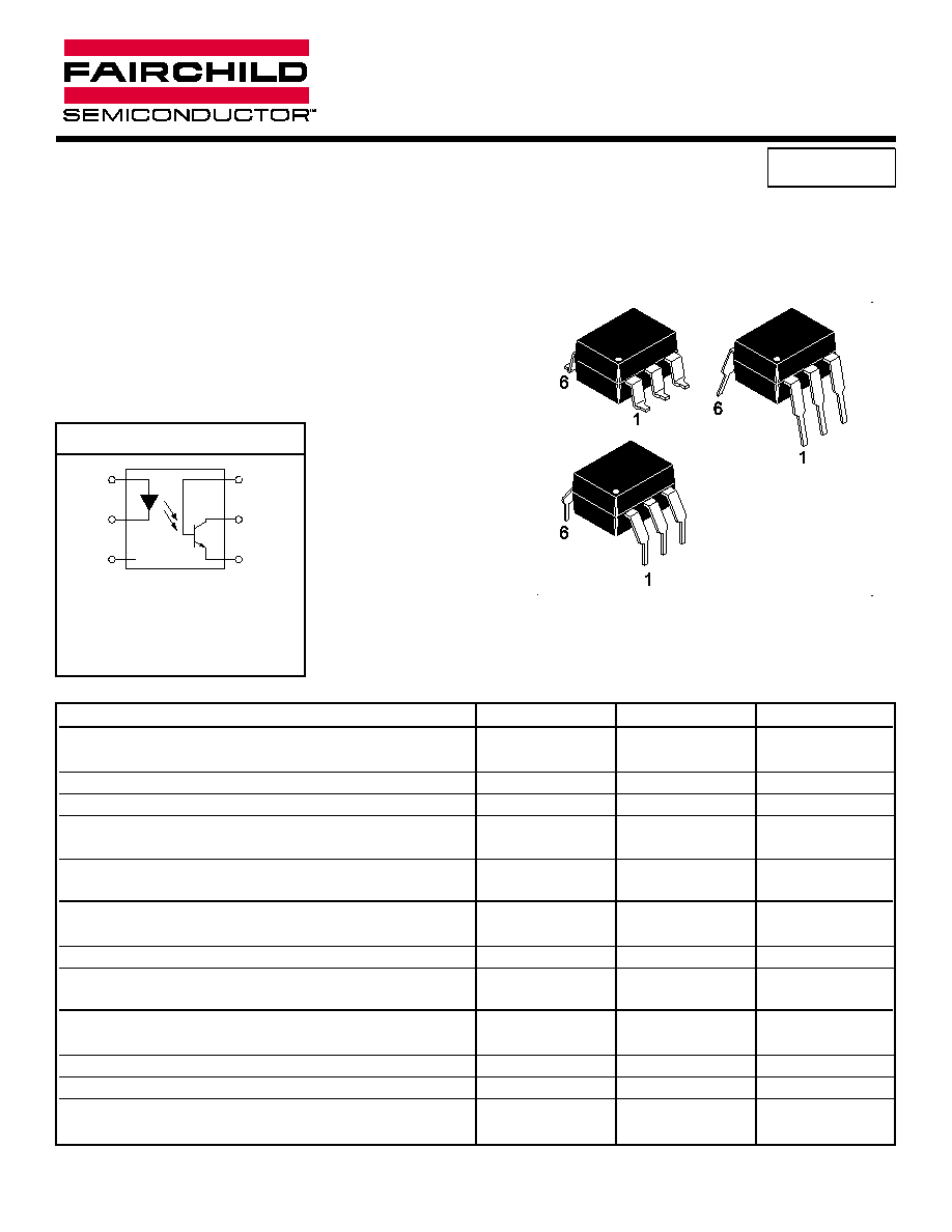
PIN 1. ANODE
2. CATHODE
3. NO CONNECTION
4. EMITTER
5. COLLECTOR
6. BASE
2
1
3
NC
5
6
4
SCHEMATIC
2001 Fairchild Semiconductor Corporation
DS300269
3/22/01
1 OF 6
www.fairchildsemi.com
Parameter
Test Conditions
Symbol
Min
Typ
(1)
Max
Unit
EMITTER
(I
F
= 10 mA)
V
F
--
1.2
15
V
Input Forward Voltage
Reverse Leakage Current
(V
R
= 6.0 V)
I
R
--
--
10
µA
Capacitance
(V = 0, f =1 MHz)
C
J
--
18
--
pF
DETECTOR
BV
CEO
400
--
--
V
Collector-Emitter Breakdown Voltage (I
C
= 1.0 mA, R
BE
= 1M
!
)
Collector-Base Breakdown Voltage
(I
C
= 100 µA)
BV
CBO
400
--
--
V
Emitter-Base Breakdown Voltage
(I
E
= 100 µA)
BV
EBO
7
--
--
V
Collector-Emitter Dark Current
T
A
= 25°C
(R
BE
= 1M
!
, V
CE
= 300 V)
I
CEO
-- --
100
nA
T
A
= 100°C
--
--
250
µA
INDIVIDUAL COMPONENT CHARACTERISTICS
ELECTRICAL CHARACTERISTICS
(T
A
= 25°C Unless otherwise specified.)
Notes
1. Alway design to the specified minimum/maximum electrical limits (where applicable).
2. Current Transfer Ratio (CTR) = I
C
/I
F
x 100%.
3. For this test LED pins 1 and 2 are common and phototransistor Pins 4,5 and 6 are common.
GENERAL PURPOSE 6-PIN
PHOTOTRANSISTOR OPTOCOUPLERS
Characteristic
Test Conditions Symbol
Min
Typ
(1)
Max
Units
Output Collector Current
(V
CE
= 10 V, I
F
= 10 mA, R
BE
= 1M
!
) I
C
(CTR)
(2)
2 (20)
--
--
mA(%)
Collector-Emitter Saturation Voltage (I
C
= 0.5 mA, I
F
= 10 mA, R
BE
= 1M
!
)
V
(SAT)
--
--
0.4
V
Input-Output Isolation Voltage
(3)
(I
I-O
1
µ
A, Time = 1min)
V
ISO
5300
--
--
V
AC(RMS)
7300
--
--
V
AC(PEAK)
Isolation Resistance
(3)
R
ISO
--
10
11
--
!
Isolation Capacitance
(1)
C
ISO
0.2
pf
Turn-On Time
(V
CC
= 10 V, I
C
= 2 mA, R
L
= 100
!
)
t
ON
--
5
--
µs
Turn-Off Time
t
OFF
--
5
--
ISOLATION CHARACTERISTICS
MOC8204
www.fairchildsemi.com
2 OF 6
3/22/01
DS300269
60
0
TA, AMBIENT TEMPERATURE (
°
C)
I CBO
, COLLECT
OR-BASE CURRENT
(
A
)
40
20
0
20
40
60
80
100
2
1.8
1.6
1.4
1.2
1
1
10
100
1000
IF, LED FORWARD CURRENT (mA)
V
F
, FORW
ARD VOL
T
AGE (VOL
TS)
25
°
C
100
°
C
TA = 55
°
C
0.005
VCE, COLLECTOREMITTER VOLTAGE (VOLTS)
I
0.01
0.05
1
5
1.0
5.0
10
40
0.1
0.5
1
5
10
50 100
300
RBE = 106
TA = 25
°
C
IF = 5 mA
IF = 10 mA
IF = 50 mA
CER
, OUTPUT CURRENT
(mA)
1
TA, AMBIENT TEMPERATURE (
°
C)
I
10
20
40
60
90
100
VCE = 300 V
CER
, DARK CURRENT
(nA)
60
120
180
240
300
RBE = 106
VCE = 10 V
IF = 50 mA
IF = 10 mA
IF = 5 mA
100
100
1000
30
50
70
80
µ
VCE = 100 V
RBE = 106
VCE = 50 V
PULSE ONLY
PULSE OR DC
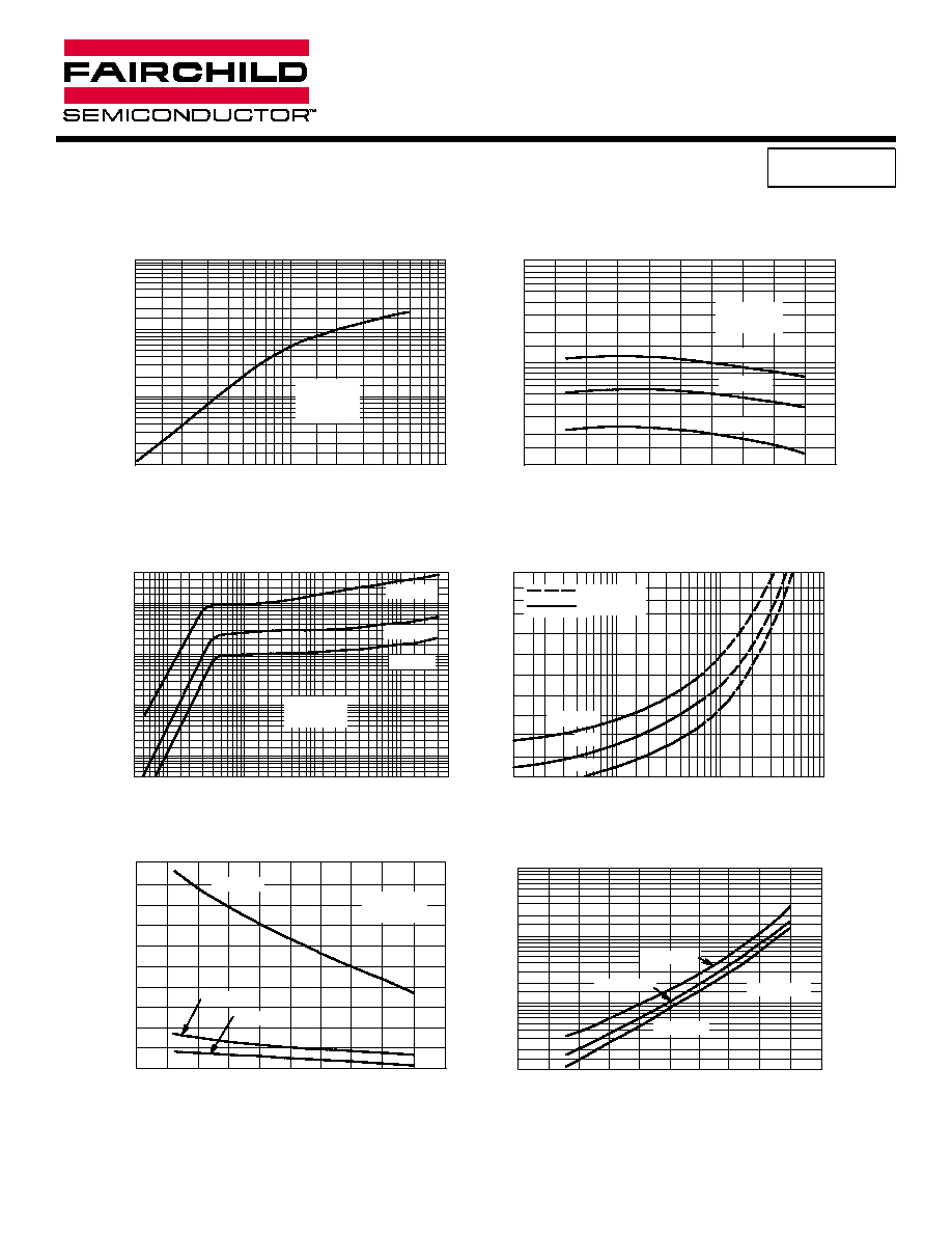
Figure 3. Output Characteristics
Figure 4. Forward Characteristics
Figure 5. CollectorBase Current versus Temperature
Figure 6. Dark Current versus Temperature
Figure 1. Output Current versus LED Input Current
0.1
1
IF, LED INPUT CURRENT (mA)
I
0.2
0.5
1
2
5
10
20
50
2
5
10
20
50
CER
, OUTPUT CURRENT
(mA)
RBE = 106
VCE = 10 V
TA = 25
°
C
1
60
TA, AMBIENT TEMPERATURE (
°
C)
I CER
, OUTPUT CURRENT
(mA)
IF = 20 mA
IF = 10 mA
IF = 5 mA
2
5
10
20
40
20
0
20
40
60
80
100
RBE = 106
VCE = 10 V
Figure 2. Output Current versus Temperature
GENERAL PURPOSE 6-PIN
PHOTOTRANSISTOR OPTOCOUPLERS
MOC8204
DS300269
3/22/01
3 OF 6
www.fairchildsemi.com
GENERAL PURPOSE 6-PIN
PHOTOTRANSISTOR OPTOCOUPLERS
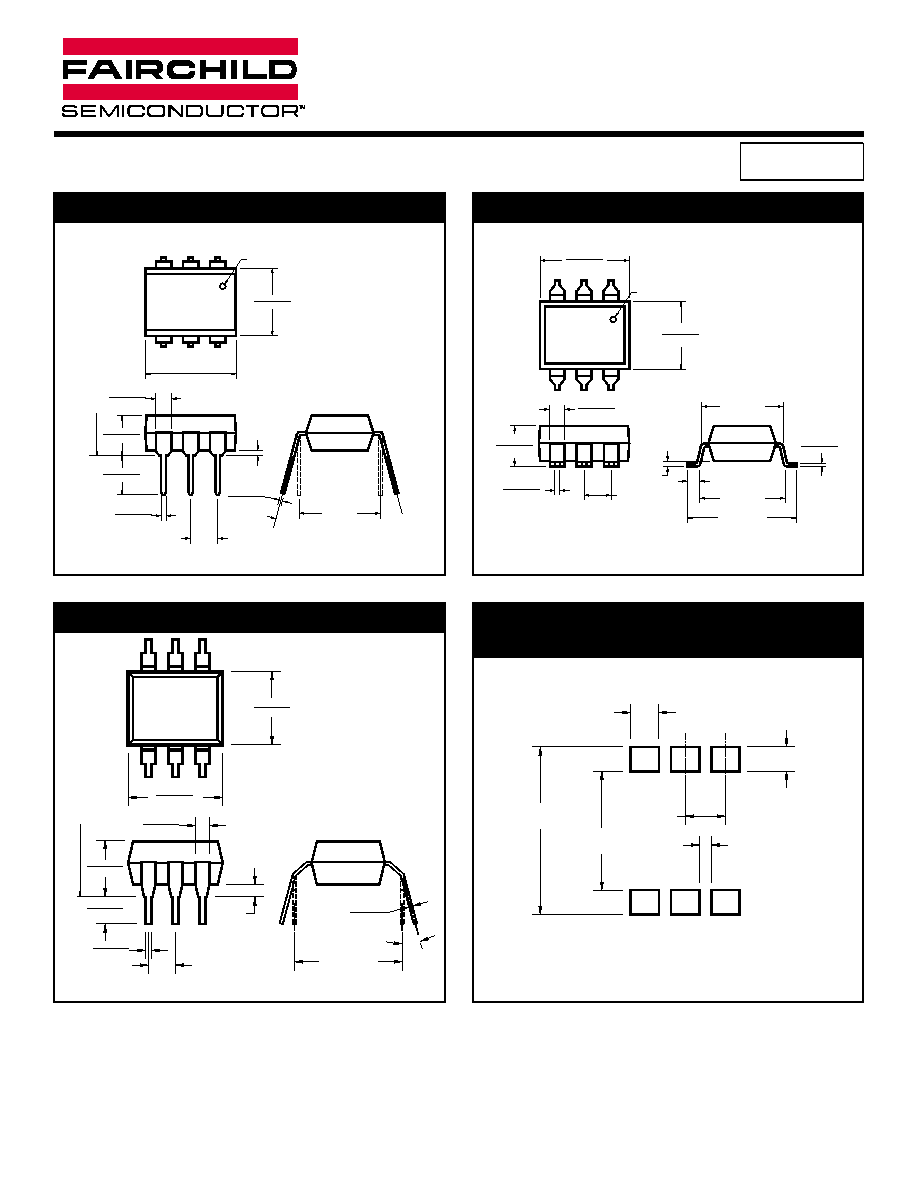
Lead Coplanarity : 0.004 (0.10) MAX
0.270 (6.86)
0.240 (6.10)
0.350 (8.89)
0.330 (8.38)
0.300 (7.62)
TYP
0.405 (10.30)
MAX
0.315 (8.00)
MIN
0.016 (0.40) MIN
2
5
PIN 1
ID.
0.016 (0.41)
0.008 (0.20)
0.100 (2.54)
TYP
0.022 (0.56)
0.016 (0.41)
0.070 (1.78)
0.045 (1.14)
0.200 (5.08)
0.165 (4.18)
4
3
0.020 (0.51)
MIN
1
6
0.100 (2.54)
TYP
0.020 (0.51)
MIN
0.350 (8.89)
0.330 (8.38)
0.270 (6.86)
0.240 (6.10)
PIN 1
ID.
0.022 (0.56)
0.016 (0.41)
0.070 (1.78)
0.045 (1.14)
0.200 (5.08)
0.135 (3.43)
0.300 (7.62)
TYP
0° to 15°
0.154 (3.90)
0.100 (2.54)
SEAT
I
N
G PL
AN
E
0.016 (0.40)
0.008 (0.20)
SEATING PLANE
0.016 (0.40)
0.008 (0.20)
0.070 (1.78)
0.045 (1.14)
0.350 (8.89)
0.330 (8.38)
0.154 (3.90)
0.100 (2.54)
0.200 (5.08)
0.135 (3.43)
0.004 (0.10)
MIN
0.270 (6.86)
0.240 (6.10)
0.400 (10.16)
TYP
0° to 15°
0.022 (0.56)
0.016 (0.41)
0.100 (2.54) TYP
0.070 (1.78)
0.060 (1.52)
0.030 (0.76)
0.100 (2.54)
0.295 (7.49)
0.415 (10.54)
Package Dimensions (Surface Mount)
Package Dimensions (Through Hole)
Package Dimensions (0.4"Lead Spacing)
Recommended Pad Layout for
Surface Mount Leadform
MOC8204
www.fairchildsemi.com
4 OF 6
3/22/01
DS300269
GENERAL PURPOSE 6-PIN
PHOTOTRANSISTOR OPTOCOUPLERS
R2
.R2
Opto Plus Reliability Conditioning
S
.S
Surface Mount Lead Bend
SD
.SD
Surface Mount; Tape and reel
SDL
.SDL
Surface Mount; Tape and reel
W
.W
0.4" Lead Spacing
300
.300
VDE 0884
300W
.300W
VDE 0884, 0.4" Lead Spacing
3S
.3S
VDE 0884, Surface Mount
3SD
.3SD
VDE 0884, Surface Mount, Tape & Reel
Option
Order Entry Idenifier
Description
4.0 ± 0.1
Ø1.55 ± 0.05
User Direction of Feed
4.0 ± 0.1
1.75 ± 0.10
7.5 ± 0.1
16.0 ± 0.3
12.0 ± 0.1
0.30 ± 0.05
13.2 ± 0.2
4.85 ± 0.20
0.1 MAX
10.30 ± 0.20
9.55 ± 0.20
Ø1.6 ± 0.1
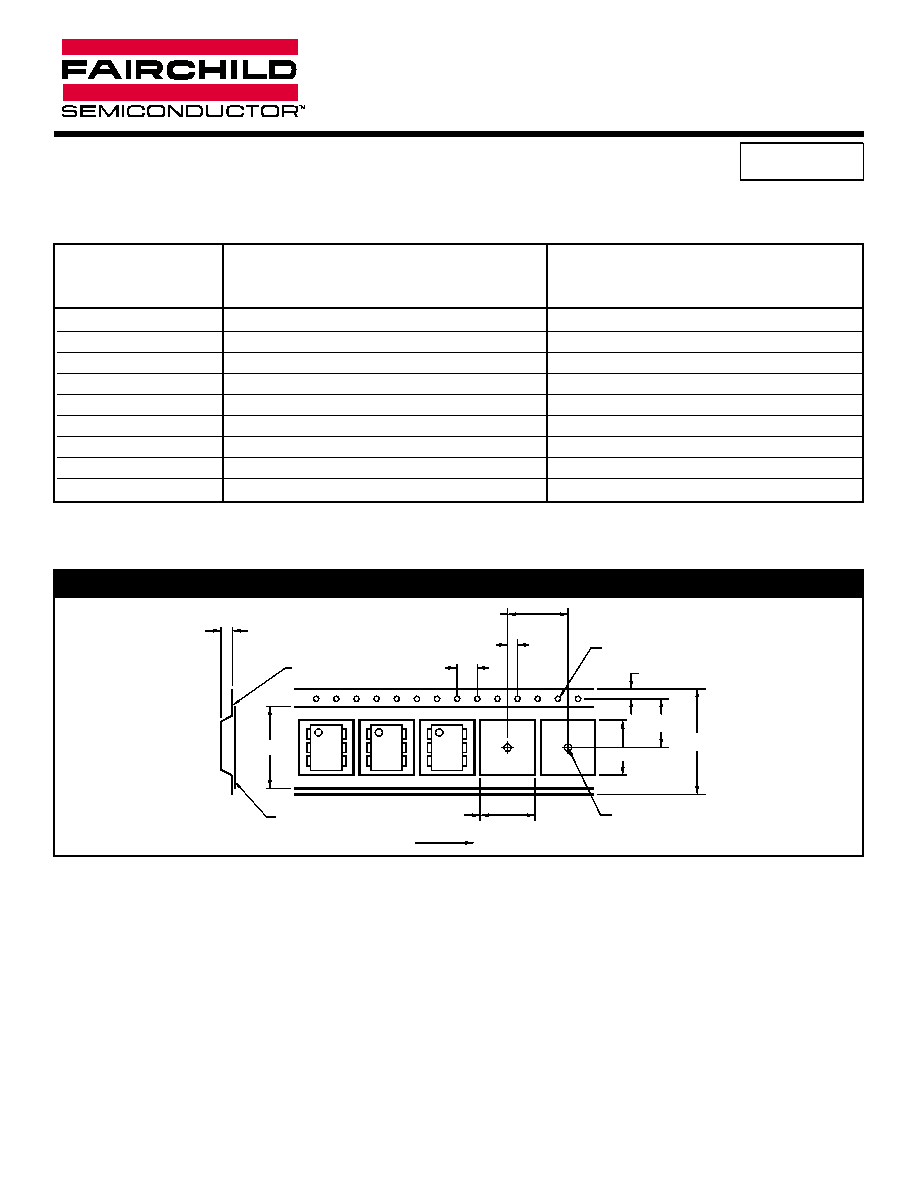
QT Carrier Tape Specifications
ORDERING INFORMATION
MOC8204
DS300269
3/22/01
5 OF 6
www.fairchildsemi.com