Äîêóìåíòàöèÿ è îïèñàíèÿ www.docs.chipfind.ru
6
1
FEATURES
· High current transfer ratio of 300%
· No base connection for improved noise immunity
· Underwriters Laboratory (UL) recognized File# E90700
DESCRIPTION
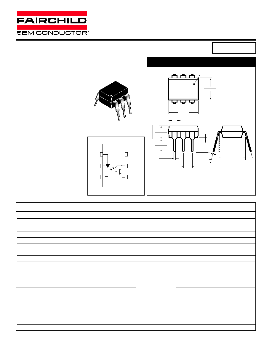
The MOC119 device has a gallium arsenide infrared emitting
diode coupled to a silicon darlington phototransistor.
PHOTODARLINGTON OPTOCOUPLERS
(NO BASE CONNECTION)
MOC119
Parameter
Symbol
Value
Units
TOTAL DEVICE
T
STG
-55 to +150
°C
Storage Temperature
Operating Temperature
T
OPR
-55 to +100
°C
Lead Solder Temperature
T
SOL
260 for 10 sec
°C
Total Device Power Dissipation @ T
A
= 25°C
P
D
250
mW
Derate above 25°C
2.94
mW/°C
Input-Output Isolation Voltage
V
ISO
5300 Vac(rms)
EMITTER
I
F
60
mA
DC/Average Forward Input Current
Reverse Input Voltage
V
R
3
V
LED Power Dissipation @ T
A
= 25°C
P
D
120
mW
Derate above 25°C
1.41
mW/°C
DETECTOR
V
CEO
30
V
Collector-Emitter Voltage
Emitter-Collector Voltage
V
ECO
7
V
Detector Power Dissipation @ T
A
= 25°C
P
D
150
mW
Derate above 25°C
1.76
mW/°C
Continuous Collector Current
I
C
150
mA
ABSOLUTE MAXIMUM RATINGS
(T
A
= 25°C Unless otherwise specified.)
PACKAGE DIMENSIONS
0.100 (2.54)
TYP
0.020 (0.51)
MIN
0.350 (8.89)
0.330 (8.38)
0.270 (6.86)
0.240 (6.10)
PIN 1
ID.
0.022 (0.56)
0.016 (0.41)
0.070 (1.78)
0.045 (1.14)
0.200 (5.08)
0.115 (2.92)
0.300 (7.62)
TYP
0° to 15°
0.154 (3.90)
0.100 (2.54)
SEATI
N
G
PL
AN
E
0.016 (0.40)
0.008 (0.20)
NOTE
All dimensions are in inches (millimeters)
APPLICATIONS
· Appliances, measuring instruments
· I/O interface for computers
· Programmable controllers
· Portable electronics
· Interfacing and coupling systems of
different potentials and impedance
· Solid state relays
EMITTER
COLLECTOR
1
2
3
ANODE
CATHODE
4
5
6 N/C
N/C
2001 Fairchild Semiconductor Corporation
DS300382
2/16/01
1 OF 5
www.fairchildsemi.com

Parameter
Test Conditions
Symbol
Min
Typ**
Max
Unit
EMITTER
(I
F
= 10 mA)
V
F
1.15
1.5
V
Input Forward Voltage
Input Capacitance
(V
R
= 0, f = 1 MHz)
C
IN
18
pF
Reverse Leakage Current
(V
R
= 3.0 V)
I
R
0.05
100
µA
DETECTOR
(I
C
= 100 µA)
BV
CEO
30
V
Collector-Emitter Breakdown Voltage
Emitter-Collector Breakdown Voltage
(I
E
= 10 µA)
BV
ECO
7
V
Collector-Emitter Dark Current
(V
CE
= 10 V)
I
CEO
100
nA
INDIVIDUAL COMPONENT CHARACTERISTICS
ELECTRICAL CHARACTERISTICS
(T
A
= 25°C Unless otherwise specified.)
DC Characteristic
Test Conditions
Symbol
Min
Typ**
Max
Units
Current Transfer Ratio,
(I
F
= 10 mA, V
CE
= 2 V)
CTR
30 (300)
45 (450)
mA (%)
TRANSFER CHARACTERISTICS
Characteristic
Test Conditions
Symbol
Min
Typ**
Max
Units
SWITCHING TIMES
t
on
3.5
µs
Turn-on Time
(V
CE
= 10 V, R
L
= 100 , I
F
= 5 mA)
Turn-off Time
t
off
95
µs
TRANSFER CHARACTERISTICS
Characteristic
Test Conditions
Symbol
Min
Typ**
Max
Units
Input-Output Isolation Voltage
(I
I-O
1 µA, 1 min.)
V
ISO
7500
Vac(pk)
(I
I-O
1 µA, 1 min.)
5300
Vac(rms)
Isolation Resistance
(V
I-O
= 500 VDC)
R
ISO
10
11
Isolation Capacitance
(V = 0 V, f = 1 MHz)
C
ISO
0.2
pf
Collector - Emitter Saturation Voltage
(I
C
= 10 mA, I
F
= 10 mA)
V
CE (SAT)
1
V
ISOLATION CHARACTERISTICS
Note
** Typical values at T
A
= 25°C
PHOTODARLINGTON OPTOCOUPLERS
(NO BASE CONNECTION)
MOC119
www.fairchildsemi.com
2 OF 5
2/16/01
DS300382
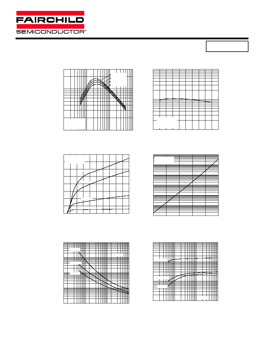
Fig. 6 Turn-Off Time vs. Input Current
I
F
- LED INPUT CURRENT (mA)
0.1
1
10
100
T
O
FF
-
TIME (µs)
1
10
100
1000
VCC = 10 V
R
L
= 100
R
L
= 1 k
R
L
= 10
Fig. 3 Collector Current vs. Collector-Emitter Voltage
V
CE
- COLLECTOR -EMITTER VOLTAGE (V)
0
1
2
3
4
5
6
7
8
9
10
I
C
- COLLECT
OR CURRENT
(NORMALIZED)
0
2
4
6
8
10
12
14
16
I
F
= 10 mA
I
F
= 5 mA
I
F
= 2 mA
I
F
= 1 mA
NORMALIZED TO:
I
F
= 1 mA
V
CE
= 5 V
Fig. 5 Turn-On Time vs. Input Current
I
F
- LED INPUT CURRENT (mA)
T
O
N
-
TIME (µs)
0.1
1
10
100
0.1
1
10
100
1000
R
L
= 100
R
L
= 1 k
R
L
= 10
VCC = 10 V
T
A
- AMBIENT TEMPERATURE (°C)
I
C
E
O
- COLLECT
OR-EMITTER DARK CURRENT
(nA)
Fig. 4 Dark Current vs. Ambient Temperature
0
20
40
60
80
100
0.01
0.1
1
10
100
1000
10000
NORMALIZED TO:
T
A
= 25°C
V
CE
= 10 V
Fig. 1 Output Current vs. Input Current
I
F
- LED INPUT CURRENT (mA)
0.1
1
10
100
CTR - CURRENT
TRANSFER RA
TIO (NORMALIZED)
0.1
1
NORMALIZED TO:
CTR @ I
F
= 10 mA
T
A
= 25°C
V
CE
= 5 V
T
A
= 0°C, 25°C
T
A
= 70°C
T
A
= 100°C
T
A
= -55°C
T
A
- AMBIENT TEMPERATURE (°C)
Fig. 2 Current Transfer Ratio vs. Ambient Temperature
-80
-60
-40
-20
0
20
40
60
80
100
120
CTR - CURRENT
TRANSFER RA
TIO (NORMALIZED)
0.1
1
10
NORMALIZED TO:
CTR @ I
F
= 10 mA
T
A
= 25°C
V
CE
= 10 V
PHOTODARLINGTON OPTOCOUPLERS
(NO BASE CONNECTION)
MOC119
DS300382
2/16/01
3 OF 5
www.fairchildsemi.com
S
.S
Surface Mount Lead Bend
SD
.SD
Surface Mount; Tape and reel
W
.W
0.4" Lead Spacing
300
.300
VDE 0884
300W
.300W
VDE 0884, 0.4" Lead Spacing
3S
.3S
VDE 0884, Surface Mount
3SD
.3SD
VDE 0884, Surface Mount, Tape & Reel
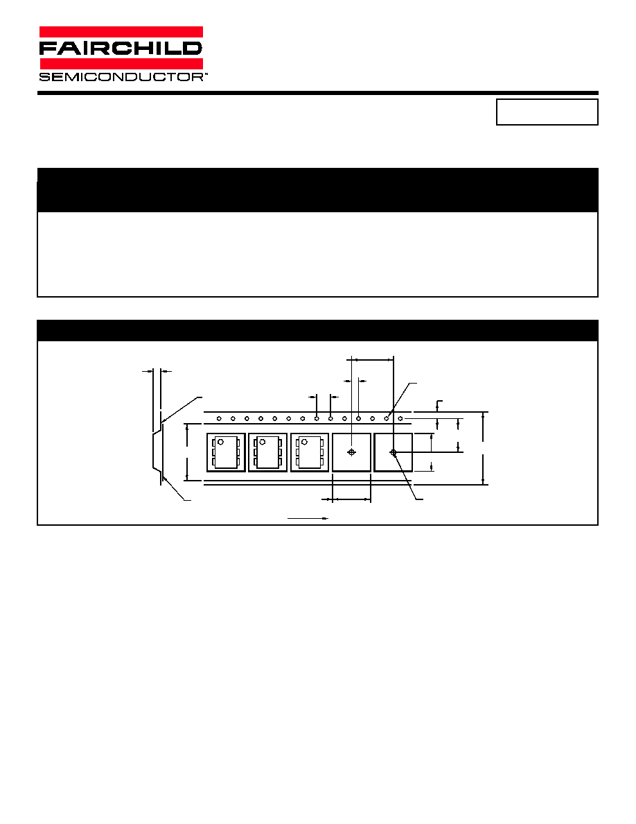
4.0 ± 0.1
Ø1.55 ± 0.05
User Direction of Feed
4.0 ± 0.1
1.75 ± 0.10
7.5 ± 0.1
16.0 ± 0.3
12.0 ± 0.1
0.30 ± 0.05
13.2 ± 0.2
4.85 ± 0.20
0.1 MAX
10.30 ± 0.20
9.55 ± 0.20
Ø1.6 ± 0.1
QT Carrier Tape Specifications ("D" Taping Orientation)
ORDERING INFORMATION
Order
Option
Entry
Description
Identifier
PHOTODARLINGTON OPTOCOUPLERS
(NO BASE CONNECTION)
MOC119
www.fairchildsemi.com
4 OF 5
2/16/01
DS300382

PHOTODARLINGTON OPTOCOUPLERS
(NO BASE CONNECTION)
DISCLAIMER
FAIRCHILD SEMICONDUCTOR RESERVES THE RIGHT TO MAKE CHANGES WITHOUT FURTHER NOTICE TO
ANY PRODUCTS HEREIN TO IMPROVE RELIABILITY, FUNCTION OR DESIGN. FAIRCHILD DOES NOT ASSUME
ANY LIABILITY ARISING OUT OF THE APPLICATION OR USE OF ANY PRODUCT OR CIRCUIT DESCRIBED
HEREIN; NEITHER DOES IT CONVEY ANY LICENSE UNDER ITS PATENT RIGHTS, NOR THE RIGHTS OF
OTHERS.
LIFE SUPPORT POLICY
FAIRCHILD'S PRODUCTS ARE NOT AUTHORIZED FOR USE AS CRITICAL COMPONENTS IN LIFE SUPPORT
DEVICES OR SYSTEMS WITHOUT THE EXPRESS WRITTEN APPROVAL OF THE PRESIDENT OF FAIRCHILD
SEMICONDUCTOR CORPORATION. As used herein:
1. Life support devices or systems are devices or
systems which, (a) are intended for surgical
implant into the body,or (b) support or sustain life,
and (c) whose failure to perform when properly
used in accordance with instructions for use provided
in labeling, can be reasonably expected to result in a
significant injury of the user.
2. A critical component in any component of a life support
device or system whose failure to perform can be
reasonably expected to cause the failure of the life
support device or system, or to affect its safety or
effectiveness.
DS300382
2/16/01
5 OF 5
www.fairchildsemi.com