
© 2000 Fairchild Semiconductor Corporation
DS005215
www.fairchildsemi.com
February 1984
Revised February 2000
MM74HC4514 4-t
o
-1
6
Li
ne D
e
coder wit
h
Lat
ch
MM74HC4514
4-to-16 Line Decoder with Latch
General Description
The MM74HC4514 utilizes advanced silicon-gate CMOS
technology, which is well suited to memory address decod-
ing or data routing application. It possesses high noise
immunity and low power dissipation usually associated with
CMOS circuitry, yet speeds comparable to low power
Schottky TTL circuits. It can drive up to 10 LS-TTL loads.
The MM74HC4514 contain a 4-to-16 line decoder and a 4-
bit latch. The latch can store the data on the select inputs,
thus allowing a selected output to remain HIGH even
though the select data has changed. When the LATCH
ENABLE input to the latches is HIGH the outputs will
change with the inputs. When LATCH ENABLE goes LOW
the data on the select inputs is stored in the latches. The
four select inputs determine which output will go HIGH pro-
vided the INHIBIT input is LOW. If the INHIBIT input is
HIGH all outputs are held LOW thus disabling the decoder.
The MM74HC4514 is functionally and pinout equivalent to
the CD4514BC and the MC1451BC. All inputs are pro-
tected against damage due to static discharge diodes from
V
CC
and ground.
Features
s
Typical propagation delay: 18 ns
s
Low quiescent power: 80
µ
A maximum (74HC Series)
s
Low input current: 1
µ
A maximum
s
Fanout of 10 LS-TTL loads (74HC Series)
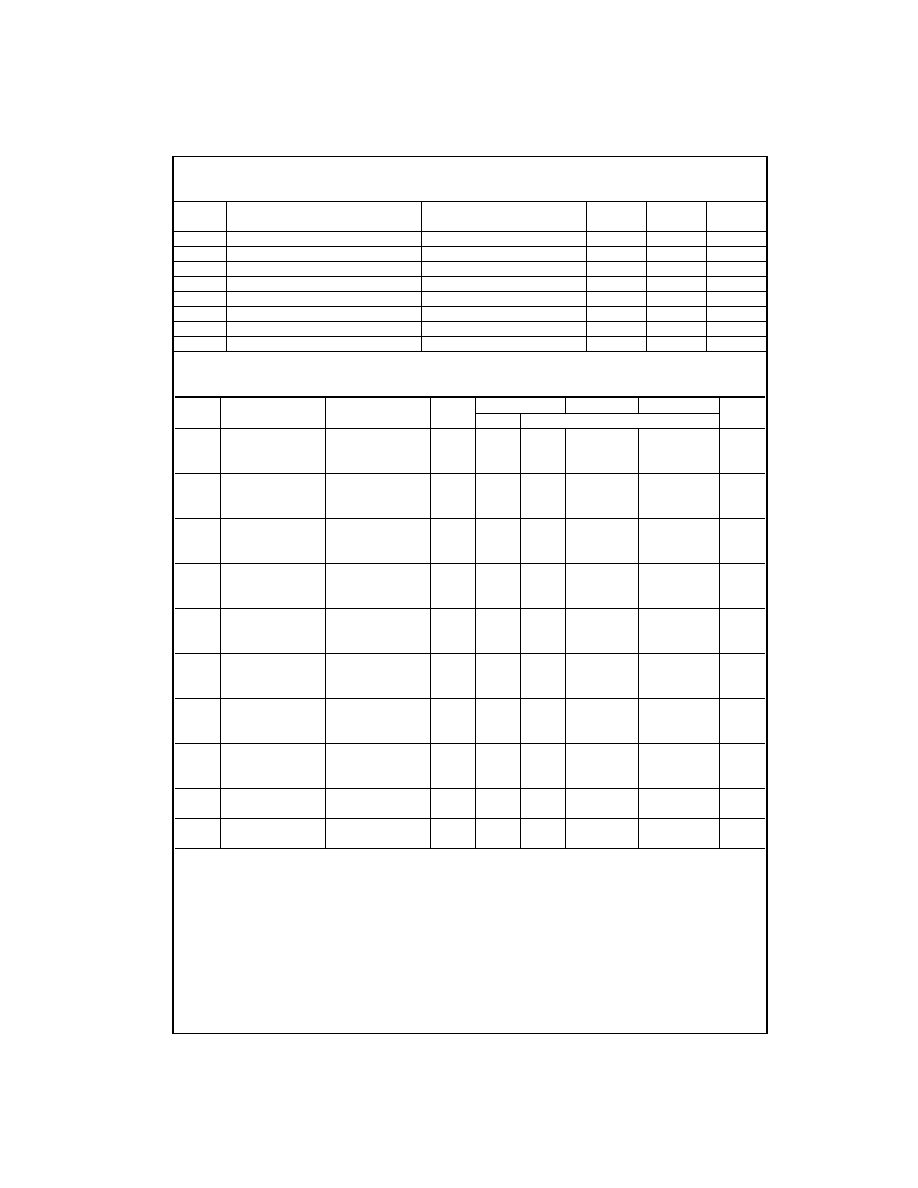
Ordering Code:
Devices also available in Tape and Reel. Specify by appending the suffix letter "X" to the ordering code.
Order Number
Package Number
Package Description
MM74HC4514WM
M24B
24-Lead Small Outline Integrated Circuit (SOIC), JEDEC MS-0013, 0.300" Wide
MM74HC4514MTC
MTC24
24-Lead Thin Shrink Small Outline Package (TSSOP), JEDEC MO-153, 4.4mm Wide
MM74HC4514N
N24C
24-Lead Plastic Dual-In-Line Package (PDIP), JEDEC MS-100, 0.300" Wide

www.fairchildsemi.com
2
M
M
74HC4514
Connection Diagram
Top View
Truth Table
Logic Diagram
Data Inputs
LE
Inhibit
D
C
B
A
Selected
Output
High
H
L
L
L
L
L
S0
H
L
L
L
L
H
S1
H
L
L
L
H
L
S2
H
L
L
L
H
H
S3
H
L
L
H
L
L
S4
H
L
L
H
L
H
S5
H
L
L
H
H
L
S6
H
L
L
H
H
H
S7
H
L
H
L
L
L
S8
H
L
H
L
L
H
S9
H
L
H
L
H
L
S10
H
L
H
L
H
H
S11
H
L
H
H
L
L
S12
H
L
H
H
L
H
S13
H
L
H
H
H
L
S14
H
L
H
H
H
H
S15
All
X
H
X
X
X
X
Outputs
=
0
Latched
L
L
X
X
X
X
Data

3
www.fairchildsemi.com
MM74HC4514
Absolute Maximum Ratings
(Note 1)
(Note 2)
Recommended Operating
Conditions
Note 1: Maximum Ratings are those values beyond which damage to the
device may occur.
Note 2: Unless otherwise specified all voltages are referenced to ground.
Note 3: Power Dissipation temperature derating -- plastic "N" package:
-
12 mW/
°
C from 65
°
C to 85
°
C.
DC Electrical Characteristics
(Note 4)
Note 4: For a power supply of 5V
±
10% the worst case output voltages (V
OH
, and V
OL
) occur for HC at 4.5V. Thus the 4.5V values should be used when
designing with this supply. Worst case V
IH
and V
IL
occur at V
CC
=
5.5V and 4.5V respectively. (The V
IH
value at 5.5V is 3.85V.) The worst case leakage cur-
rent (I
IN
, I
CC
, and I
OZ
) occur for CMOS at the higher voltage and so the 6.0V values should be used.
Supply Voltage (V
CC
)
-
0.5 to
+
7.0V
DC Input Voltage (V
IN
)
-
1.5 to V
CC
+
1.5V
DC Output Voltage (V
OUT
)
-
0.5 to V
CC
+
0.5V
Clamp Diode Current (I
IK
, I
OK
)
±
20 mA
DC Output Current, per pin (I
OUT
)
±
25 mA
DC V
CC
or GND Current, per pin (I
CC
)
±
50 mA
Storage Temperature Range (T
STG
)
-
65
°
C to
+
150
°
C
Power Dissipation (P
D
)
(Note 3)
600 mW
S.O. Package only
500 mW
Lead Temperature (T
L
)
(Soldering 10 seconds)
260
°
C
Min
Max
Units
Supply Voltage (V
CC
)
2
6
V
DC Input or Output Voltage
0
V
CC
V
(V
IN
, V
OUT
)
Operating Temperature Range (T
A
)
-
40
+
85
°
C
Input Rise or Fall Times
(t
r
, t
f
) V
CC
=
2.0V
1000
ns
V
CC
=
4.5V
500
ns
V
CC
=
6.0V
400
ns
Symbol
Parameter
Conditions
V
CC
T
A
=
25
°
C
T
A
=
-
40 to 85
°
C T
A
=
-
55 to 125
°
C
Units
Typ
Guaranteed Limits
V
IH
Minimum HIGH Level
2.0V
1.5
1.5
1.5
V
Input Voltage
4.5V
3.15
3.15
3.15
6.0V
4.2
4.2
4.2
V
IL
Maximum LOW Level
2.0V
0.5
0.5
0.5
V
Input Voltage
4.5V
1.35
1.35
1.35
6.0V
1.8
1.8
1.8
V
OH
Minimum HIGH Level
V
IN
=
V
IH
or V
IL
2.0V
2.0
1.9
1.9
1.9
Output Voltage
|I
OUT
|
20
µ
A
4.5V
4.5
4.4
4.4
4.4
V
6.0V
6.0
5.9
5.9
5.9
V
IN
=
V
IH
or V
IL
|I
OUT
|
4.0 mA
4.5V
4.2
3.98
3.84
3.7
V
|I
OUT
|
5.2 mA
6.0V
5.7
5.48
5.34
5.2
V
OL
Maximum LOW Level
V
IN
=
V
IH
or V
IL
2.0V
0
0.1
0.1
0.1
Output Voltage
|I
OUT
|
20
µ
A
4.5V
0
0.1
0.1
0.1
V
6.0V
0
0.1
0.1
0.1
V
IN
=
V
IH
or V
IL
|I
OUT
|
4.0 mA
4.5V
0.2
0.26
0.33
0.4
V
|I
OUT
|
5.2 mA
6.0V
0.2
0.26
0.33
0.4
I
IN
Maximum Input Current
V
IN
=
V
CC
or GND
6.0V
±
0.1
±
1.0
±
1.0
µ
A
I
CC
Maximum Quiescent
V
IN
=
V
CC
or GND
6.0V
8.0
80
160
µ
A
Supply Current
I
OUT
=
0
µ
A
www.fairchildsemi.com
4
M
M
74HC4514
AC Electrical Characteristics
V
CC
=
5V, T
A
=
25
°
C, C
L
=
15 pF, t
r
=
t
f
=
6 ns
AC Electrical Characteristics
V
CC
=
2.0V
-
6.0V, C
L
=
50 pF, t
r
=
t
f
=
6 ns (unless otherwise specified)
Note 5: C
PD
determines the no load dynamic power consumption, P
D
=
C
PD
V
CC
2
f
+
I
CC
V
CC
, and the no load dynamic current consumption,
I
S
=
C
PD
V
CC
f
+
I
CC
.
Symbol
Parameter
Conditions
Typ
Guaranteed
Units
Limit
t
PHL
, t
PLH
Maximum Propagation Delay Data to Output
18
30
ns
t
PHL
Maximum Propagation Delay LE to Output
18
30
ns
t
PLH
Maximum Propagation Delay LE to Output
24
40
ns
t
PHL
Maximum Propagation Delay Inhibit to Output
16
30
ns
t
PLH
Maximum Propagation Delay Inhibit to Output
24
40
ns
t
s
Minimum Setup Time, Date to LE
20
ns
t
H
Minimum Hold Time, LE to Data
5
ns
t
W
Minimum Pulse Width, Latch Enable
16
ns
Symbol
Parameter
Conditions
V
CC
T
A
=
25
°
C
T
A
=
-
40 to 85
°
C T
A
=
-
55 to 125
°
C
Units
Typ
Guaranteed Limits
t
PHL
, t
PLH
Maximum Propagation
2.0V
80
175
220
263
ns
Delay Data to Output
4.5V
18
35
44
53
6.0V
16
30
38
45
t
PHL
Maximum Propagation
2.0V
80
175
220
263
ns
Delay LE to Output
4.5V
19
35
44
53
6.0V
17
30
38
45
t
PLH
Maximum Propagation
2.0V
120
230
290
343
ns
Delay LE to Output
4.5V
27
46
58
69
6.0V
22
39
49
58
t
PHL
Maximum Propagation
2.0V
70
175
220
263
ns
Delay Inhibit to Output
4.5V
18
35
44
53
6.0V
16
30
38
45
t
PLH
Maximum Propagation
2.0V
120
230
290
343
ns
Delay Inhibit to Output
4.5V
27
46
58
69
6.0V
22
39
49
58
t
s
Minimum Setup Time,
2.0V
100
125
150
ns
Data to LE
4.5V
20
25
30
6.0V
17
21
25
t
H
Minimum Hold Time,
2.0V
5
5
5
ns
LE to Data
4.5V
5
5
5
6.0V
5
5
5
t
W
Minimum Pulse Width,
2.0V
80
100
120
ns
Latch Enable
4.5V
16
20
24
6.0V
14
17
20
C
PD
Power Dissipation
290
pF
Capacitance (Note 5)
C
IN
Maximum Input
5
10
10
10
pF
Capacitance

5
www.fairchildsemi.com
MM74HC4514
Physical Dimensions
inches (millimeters) unless otherwise noted
24-Lead Small Outline Integrated Circuit (SOIC), JEDEC MS-013, 0.300" Wide
Package Number M24B