
October 1987
Revised January 1999
MM74C901
·
MM74C902 He
x In
ver
ti
ng
T
TL
Buf
f
e
r
· H
e
x N
o
n-I
n
ve
r
t
ing TTL B
u
ff
e
r
© 1999 Fairchild Semiconductor Corporation
DS005909.prf
www.fairchildsemi.com
MM74C901 · MM74C902
Hex Inverting TTL Buffer ·
Hex Non-Inverting TTL Buffer
General Description
The MM74C901 and MM74C902 hex buffers employ com-
plementary MOS to achieve wide supply operating range,
low power consumption, and high noise immunity. These
buffers provide direct interface from PMOS into CMOS or
TTL and direct interface from CMOS to TTL or CMOS
operating at a reduced V
CC
supply.
Features
s
Wide supply voltage range:
3.0V to 15V
s
Guaranteed noise margin:
1.0V
s
High noise immunity:
0.45 V
CC
(typ.)
s
TTL compatibility:
Fan out of 2 driving standard TTL
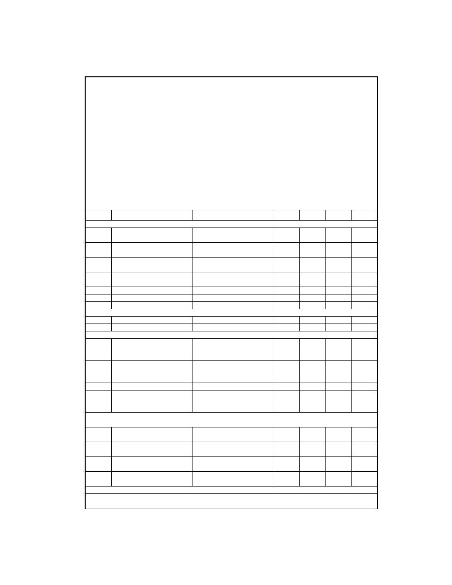
Ordering Code:
Devices also available in Tape and Reel. Specify by appending the suffix letter "X" to the ordering code.
Connection Diagrams
Pin Assignments for DIP and SOIC
MM74C901
Top View
MM74C902
Top View
Logic Diagrams
MM74C901
CMOS to TTL Inverting Buffer
MM74C902
CMOS to TTL Buffer
Order Number
Package Number
Package Description
MM74C901M
M14A
14-Lead Small Outline Integrated Circuit (SOIC), JEDEC MS-120, 0.150" Narrow
MM74C901N
N14A
14-Lead Plastic Dual-In-Line Package (PDIP), JEDEC MS-011, 0.300" Wide
MM74C902M
M14A
14-Lead Small Outline Integrated Circuit (SOIC), JEDEC MS-120, 0.150" Narrow
MM74C902N
N14A
14-Lead Plastic Dual-In-Line Package (PDIP), JEDEC MS-011, 0.300" Wide
www.fairchildsemi.com
2
MM
74
C
9
0
1
· M
M
74C902
Absolute Maximum Ratings
(Note 1)
Note 1: "Absolute Maximum Ratings" are those values beyond which the
safety of the device cannot be guaranteed. Except for "Operating Tempera-
ture Range" they are not meant to imply that the devices should be oper-
ated at these limits. The table of "Electrical Characteristics" provides
conditions for actual device operation.
DC Electrical Characteristics
Min/Max limits apply across temperature range unless otherwise noted
Voltage at Any Pin
-
0.3V to V
CC
+
0.3V
Voltage at Any Input Pin
MM74C901
-
0.3V to
+
15V
MM74C902
-
0.3V to
+
15V
Storage Temperature Range (T
S
)
-
65
°
C to
+
150
°
C
Power Dissipation (P
D
)
Dual-In-Line 700
mW
Small Outline
500 mW
Operating Temperature Range (T
A
)
MM74C901, MM74C902,
-
40
°
C to
+
85
°
C
Operating V
CC
Range
3.0V to 15V
Absolute Maximum V
CC
18V
Lead Temperature (T
L
)
(Soldering, 10 seconds)
260
°
C
Symbol Parameter
Conditions Min
Typ
Max
Units
CMOS TO CMOS
V
IN(1)
Logical "1" Input Voltage
V
CC
=
5.0V
3.5
V
V
CC
=
10V
8.0
V
V
IN(0)
Logical "0" Input Voltage
V
CC
=
5.0V
1.5
V
V
CC
=
10V
2.0
V
V
OUT(1)
Logical "1" Output Voltage
V
CC
=
5.0V, I
O
=
-
10
µ
A
4.5
V
V
CC
=
10V, I
O
=
-
10
µ
A
9.0
V
V
OUT(0)
Logical "0" Output Voltage
V
CC
=
5.0V
0.5
V
V
CC
=
10V
1.0
V
I
IN(1)
Logical "1" Input Current
V
CC
=
15V, V
IN
=
15V
0.005
1.0
µ
A
I
IN(0)
Logical "0" Input Current
V
CC
=
15V, V
IN
=
0V
-
1.0
-
0.005
µ
A
I
CC
Supply Current
V
CC
=
15V
0.05
15
µ
A
TTL TO CMOS
V
IN(1)
Logical "1" Input Voltage
V
CC
=
4.75V
V
CC
-
1.5
V
V
IN(0)
Logical "0" Input Voltage
V
CC
=
4.75V
0.8
V
CMOS TO TTL
V
IN(1)
Logical "1" Input Voltage
MM74C901 V
CC
=
4.75V
4.25
V
MM74C902 V
CC
=
4.75V
V
CC
-
1.5
V
V
IN(0)
Logical "0" Input Voltage
MM74C901 V
CC
=
4.75V
1.0
V
MM74C902 V
CC
=
4.75V
1.5
V
V
OUT(1)
Logical "1" Output Voltage
V
CC
=
4.75V, I
O
=
-
800
µ
A
2.4
V
V
OUT(0)
Logical "0" Output Voltage
MM74C901 V
CC
=
4.75V, I
O
=
2.6 mA
0.4
V
MM74C902 V
CC
=
4.75V, I
O
=
3.2 mA
0.4
V
OUTPUT DRIVE (See Family Characteristics Data Sheet) (Short Circuit Current)
(MM74C901)
I
SOURCE
Output Source Current
V
CC
=
5.0V, V
OUT
=
0V
-
5.0 mA
(P-Channel) T
A
=
25
°
C, V
IN
=
0V
I
SOURCE
Output Source Current
V
CC
=
10V, V
OUT
=
0V
-
20 mA
(P-Channel) T
A
=
25
°
C, V
IN
=
0V
I
SINK
Output Sink Current
V
CC
=
5.0V, V
OUT
=
V
CC
9.0 mA
(N-Channel) T
A
=
25
°
C, V
IN
=
V
CC
I
SINK
Output Sink Current
V
CC
=
5.0V, V
OUT
=
0.4V
3.8
mA
(N-Channel) T
A
=
25
°
C, V
IN
=
V
CC
(MM74C902)
3
www.fairchildsemi.com
MM74C901
· MM74C902
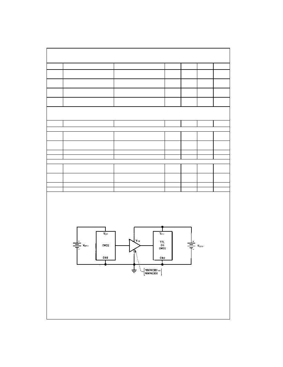
DC Electrical Characteristics
(Continued)
AC Electrical Characteristics
(Note 2)
T
A
=
25
°
C, C
L
=
50 pF, unless otherwise noted
Note 2: AC Parameters are guaranteed by DC correlated testing.
Note 3: Capacitance is guaranteed by periodic testing.
Note 4: C
PD
determines the no load AC power consumption of any CMOS device. For complete explanation see Family Characteristics application note
AN-90.
Typical Application
CMOS to TTL or CMOS at a Lower V
CC
Note: V
CC1
=
V
CC2
Symbol Parameter
Conditions Min
Typ
Max
Units
I
SOURCE
Output Source Current
V
CC
=
5.0V, V
OUT
=
0V
-
5.0 mA
(P-Channel) T
A
=
25
°
C, V
IN
=
V
CC
I
SOURCE
Output Source Current
V
CC
=
10V, V
OUT
=
0V
-
20 mA
(P-Channel) T
A
=
25
°
C, V
IN
=
V
CC
I
SINK
Output Sink Current
V
CC
=
5.0V, V
OUT
=
V
CC
9.0 mA
(N-Channel) T
A
=
25
°
C, V
IN
=
0V
I
SINK
Output Sink Current
V
CC
=
5.0V, V
OUT
=
0.4V
3.8
mA
(N-Channel) T
A
=
25
°
C, V
IN
=
0V
Symbol Parameter
Conditions Min
Typ
Max
Units
MM74C901
t
pd1
Propagation Delay Time
V
CC
=
5.0V
38
70
ns
to a Logical "1"
V
CC
=
10V
22
30
ns
t
pd0
Propagation Delay Time
V
CC
=
5.0V
21
35
ns
to a Logical "0"
V
CC
=
10V
13
20
ns
C
IN
Input Capacitance
Any Input (Note 3)
14
pF
C
PD
Power Dissipation Capacity
Per Buffer (Note 4)
30
pF
MM74C902
t
pd1
Propagation Delay Time
V
CC
=
5.0V
57
90
ns
to a Logical "1"
V
CC
=
10V
27
40
ns
t
pd0
Propagation Delay Time
V
CC
=
5.0V
54
90
ns
to a Logical "0"
V
CC
=
10V
25
40
ns
C
IN
Input Capacitance
Any Input (Note 3)
5.0
pF
C
PD
Power Dissipation Capacity
Per Buffer (Note 4)
50
pF
www.fairchildsemi.com
4
MM
74
C
9
0
1
· M
M
74C902
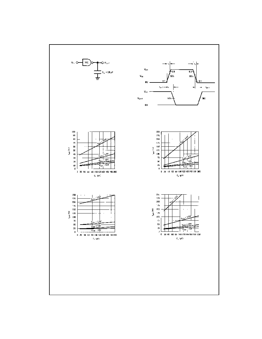
AC Test Circuit and Switching Time Waveforms
Note: Delays measured with input t
r
, t
f
=
20 ns.
CMOS to CMOS
Typical Performance Characteristics
Typical Propagation Delay to a Logical "0" for the
MM74C901
Typical Propagation Delay to a Logical "1" for the
MM74C901
Typical Propagation Delay to a Logical "0" for the
MM74C902
Typical Propagation Delay to a Logical "1" for the
MM74C902

5
www.fairchildsemi.com
MM74C901
· MM74C902
Physical Dimensions
inches (millimeters) unless otherwise noted
14-Lead Plastic Dual-In-Line Package (PDIP), JEDEC MS-120, 0.150" Narrow
Package Number M14A