
© 2000 Fairchild Semiconductor Corporation
DS009817
www.fairchildsemi.com
October 1988
Revised March 2000
DM74LS47 BCD
t
o
7-
Segment Decoder
/Dri
ver wit
h
Open-
Coll
ect
or O
u
tput
s
DM74LS47
BCD to 7-Segment Decoder/Driver with
Open-Collector Outputs
General Description
The DM74LS47 accepts four lines of BCD (8421) input
data, generates their complements internally and decodes
the data with seven AND/OR gates having open-collector
outputs to drive indicator segments directly. Each segment
output is guaranteed to sink 24 mA in the ON (LOW) state
and withstand 15V in the OFF (HIGH) state with a maxi-
mum leakage current of 250
µ
A. Auxiliary inputs provided
blanking, lamp test and cascadable zero-suppression func-
tions.
Features
s
Open-collector outputs
s
Drive indicator segments directly
s
Cascadable zero-suppression capability
s
Lamp test input
Ordering Code:
Devices also available in Tape and Reel. Specify by appending the suffix letter "X" to the ordering code.
Logic Symbol
V
CC
=
Pin 16
GND
=
Pin 8
Connection Diagram
Pin Descriptions
Note 1: OC--Open Collector
Order Number
Package Number
Package Description
DM74LS47M
M16A
16-Lead Small Outline Integrated Circuit (SOIC), JEDEC MS-012, 0.150 Narrow
DM74LS47N
N16E
16-Lead Plastic Dual-In-Line Package (PDIP), JEDEC MS-001, 0.300 Wide
Pin Names
Description
A0A3
BCD Inputs
RBI
Ripple Blanking Input (Active LOW)
LT
Lamp Test Input (Active LOW)
BI/RBO
Blanking Input (Active LOW) or
Ripple Blanking Output (Active LOW)
a g
Segment Outputs (Active LOW) (Note 1)

www.fairchildsemi.com
2
D
M
74LS47
Truth Table
Note 2: BI/RBO is wire-AND logic serving as blanking input (BI) and/or ripple-blanking output (RBO). The blanking out (BI) must be open or held at a HIGH
level when output functions 0 through 15 are desired, and ripple-blanking input (RBI) must be open or at a HIGH level if blanking or a decimal 0 is not
desired. X
=
input may be HIGH or LOW.
Note 3: When a LOW level is applied to the blanking input (forced condition) all segment outputs go to a HIGH level regardless of the state of any other input
condition.
Note 4: When ripple-blanking input (RBI) and inputs A0, A1, A2 and A3 are LOW level, with the lamp test input at HIGH level, all segment outputs go to a
HIGH level and the ripple-blanking output (RBO) goes to a LOW level (response condition).
Note 5: When the blanking input/ripple-blanking output (BI/RBO) is OPEN or held at a HIGH level, and a LOW level is applied to lamp test input, all segment
outputs go to a LOW level.
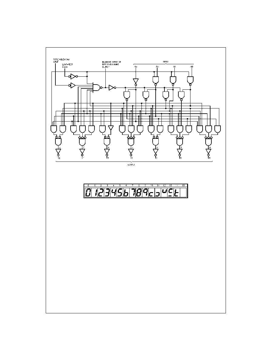
Functional Description
The DM74LS47 decodes the input data in the pattern indi-
cated in the Truth Table and the segment identification
illustration. If the input data is decimal zero, a LOW signal
applied to the RBI blanks the display and causes a multi-
digit display. For example, by grounding the RBI of the
highest order decoder and connecting its BI/RBO to RBI of
the next lowest order decoder, etc., leading zeros will be
suppressed. Similarly, by grounding RBI of the lowest order
decoder and connecting its BI/RBO to RBI of the next high-
est order decoder, etc., trailing zeros will be suppressed.
Leading and trailing zeros can be suppressed simulta-
neously by using external gates, i.e.: by driving RBI of a
intermediate decoder from an OR gate whose inputs are
BI/RBO of the next highest and lowest order decoders. BI/
RBO also serves as an unconditional blanking input. The
internal NAND gate that generates the RBO signal has a
resistive pull-up, as opposed to a totem pole, and thus BI/
RBO can be forced LOW by external means, using wired-
collector logic. A LOW signal thus applied to BI/RBO turns
off all segment outputs. This blanking feature can be used
to control display intensity by varying the duty cycle of the
blanking signal. A LOW signal applied to LT turns on all
segment outputs, provided that BI/RBO is not forced LOW.
Decimal
Inputs
Outputs
or
Note
Function
LT
RBI
A3
A2
A1
A0
BI/RBO
a
b
c
d
e
f
g
0
H
H
L
L
L
L
H
L
L
L
L
L
L
H
(Note 2)
1
H
X
L
L
L
H
H
H
L
L
H
H
H
H
(Note 2)
2
H
X
L
L
H
L
H
L
L
H
L
L
H
L
3
H
X
L
L
H
H
H
L
L
L
L
H
H
L
4
H
X
L
H
L
L
H
H
L
L
H
H
L
L
5
H
X
L
H
L
H
H
L
H
L
L
H
L
L
6
H
X
L
H
H
L
H
H
H
L
L
L
L
L
7
H
X
L
H
H
H
H
L
L
L
H
H
H
H
8
H
X
H
L
L
L
H
L
L
L
L
L
L
L
9
H
X
H
L
L
H
H
L
L
L
H
H
L
L
10
H
X
H
L
H
L
H
H
H
H
L
L
H
L
11
H
X
H
L
H
H
H
H
H
L
L
H
H
L
12
H
X
H
H
L
L
H
H
L
H
H
H
L
L
13
H
X
H
H
L
H
H
L
H
H
L
H
L
L
14
H
X
H
H
H
L
H
H
H
H
L
L
L
L
15
H
X
H
H
H
H
H
H
H
H
H
H
H
H
BI
X
X
X
X
X
X
L
H
H
H
H
H
H
H
(Note 3)
RBI
H
L
L
L
L
L
L
H
H
H
H
H
H
H
(Note 4)
LT
L
X
X
X
X
X
H
L
L
L
L
L
L
L
(Note 5)
3
www.fairchildsemi.com
DM74LS47
Logic Diagram
Numerical Designations--Resultant Displays

www.fairchildsemi.com
4
D
M
74LS47
Absolute Maximum Ratings
(Note 6)
Note 6: The "Absolute Maximum Ratings" are those values beyond which
the safety of the device cannot be guaranteed. The device should not be
operated at these limits. The parametric values defined in the Electrical
Characteristics tables are not guaranteed at the absolute maximum ratings.
The "Recommended Operating Conditions" table will define the conditions
for actual device operation.
Recommended Operating Conditions
Note 7: OFF-State at ag.
Electrical Characteristics
Over recommended operating free air temperature range (unless otherwise noted)
Note 8: All typicals are at V
CC
=
5V, T
A
=
25
°
C.
Note 9: Not more than one output should be shorted at a time, and the duration should not exceed one second.
Switching Characteristics
at V
CC
=
+
5.0V, T
A
=
+
25
°
C
Note 10: LT
=
HIGH, A0A3
=
LOW
Supply Voltage
7V
Input Voltage
7V
Operating Free Air Temperature Range
0
°
C to
+
70
°
C
Storage Temperature Range
-
65
°
C to
+
150
°
C
Symbol
Parameter
Min
Nom
Max
Units
V
CC
Supply Voltage
4.75
5
5.25
V
V
IH
HIGH Level Input Voltage
2
V
V
IL
LOW Level Input Voltage
0.8
V
I
OH
HIGH Level Output Current
-
250
µ
A
a
-
g @ 15V
=
V
OH
(Note 7)
I
OH
HIGH Level Output Current BI /RBO
-
50
µ
A
I
OL
LOW Level Output Current
24
mA
T
A
Free Air Operating Temperature
0
70
°
C
Symbol
Parameter
Conditions
Min
Typ
Max
Units
(Note 8)
V
I
Input Clamp Voltage
V
CC
=
Min, I
I
=
-
18 mA
-
1.5
V
V
OH
HIGH Level
V
CC
=
Min, I
OH
=
Max,
2.7
3.4
V
Output Voltage
V
IL
=
Max, BI /RBO
I
OFF
Output HIGH Current Segment Outputs
V
CC
=
5.5V, V
O
=
15V a
-
g
250
µ
A
V
OL
LOW Level
V
CC
=
Min, I
OL
=
Max,
0.35
0.5
Output Voltage
V
IH
=
Min, a
-
g
I
OL
=
3.2 mA, BI /RBO
0.5
V
I
OL
=
12 mA, a g
0.25
0.4
I
OL
=
1.6 mA, BI /RBO
0.4
I
I
Input Current @ Max
V
CC
=
Max, V
I
=
7V
100
µ
A
Input Voltage
V
CC
=
Max, V
I
=
10V
I
IH
HIGH Level Input Current
V
CC
=
Max, V
I
=
2.7V
20
µ
A
I
IL
LOW Level Input Current
V
CC
=
Max, V
I
=
0.4V
-
0.4
mA
I
OS
Short Circuit
V
CC
=
Max (Note 9),
mA
Output Current
I
OS
at BI/RBO
-
0.3
-
2.0
I
CC
Supply Current
V
CC
=
Max
13
mA
R
L
=
665
Symbol
Parameter
Conditions
C
L
=
15 pF
Units
Min
Max
t
PLH
Propagation Delay
100
ns
t
PHL
An to a g
100
t
PLH
Propagation Delay
100
ns
t
PHL
RBI to a g (Note 10)
100

5
www.fairchildsemi.com
DM74LS47
Physical Dimensions
inches (millimeters) unless otherwise noted
16-Lead Small Outline Integrated Circuit (SOIC), JEDEC MS-012, 0.150 Narrow
Package Number M16A