
© 2000 Fairchild Semiconductor Corporation
DS006415
www.fairchildsemi.com
August 1986
Revised March 2000
DM74LS251
3-
ST
A
T
E
1-of
-8
Li
ne Dat
a
Sel
ect
or/
M
ul
t
i
pl
exer
DM74LS251
3-STATE 1-of-8 Line Data Selector/Multiplexer
General Description
These data selectors/multiplexers contain full on-chip
binary decoding to select one-of-eight data sources, and
feature a strobe-controlled 3-STATE output. The strobe
must be at a low logic level to enable these devices. The 3-
STATE outputs permit direct connection to a common bus.
When the strobe input is HIGH, both outputs are in a high-
impedance state in which both the upper and lower transis-
tors of each totem-pole output are OFF, and the output nei-
ther drives nor loads the bus significantly. When the strobe
is LOW, the outputs are activated and operate as standard
TTL totem-pole outputs.
To minimize the possibility that two outputs will attempt to
take a common bus to opposite logic levels, the output con-
trol circuitry is designed so that the average output disable
time is shorter than the average output enable time.
Features
s
3-STATE version of DM74LS151
s
Interface directly with system bus
s
Perform parallel-to-serial conversion
s
Permit multiplexing from N-lines to one line
s
Complementary outputs provide true and inverted data
s
Maximum number of common outputs: 129
s
Typical propagation delay time (D to Y): 17 ns
s
Typical power dissipation: 35 mW
Ordering Code:
Devices also available in Tape and Reel. Specify by appending the suffix letter "X" to the ordering code.
Connection Diagram
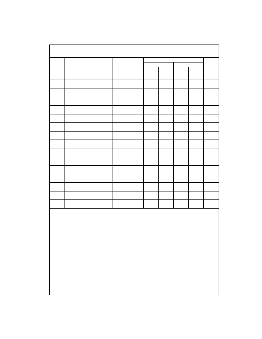
Function Table
H
=
HIGH Logic Level
L
=
LOW Logic Level
X
=
Don't Care
Z
=
High Impedance (OFF)
D0, D1...D7
=
The level of the respective D input
Order Number
Package Number
Package Description
DM74LS251M
M16A
16-Lead Small Outline Integrated Circuit (SOIC), JEDEC MS-012, 0.150 Narrow
DM74LS251N
N16E
16-Lead Plastic Dual-In-Line Package (PDIP), JEDEC MS-001, 0.300 Wide
Inputs
Outputs
Select
Strobe
Y
W
C
B
A
S
X
X
X
H
Z
Z
L
L
L
L
D0
D0
L
L
H
L
D1
D1
L
H
L
L
D2
D2
L
H
H
L
D3
D3
H
L
L
L
D4
D4
H
L
H
L
D5
D5
H
H
L
L
D6
D6
H
H
H
L
D7
D7

www.fairchildsemi.com
2
DM74LS251
Logic Diagram

3
www.fairchildsemi.com
DM74LS251
Absolute Maximum Ratings
(Note 1)
Note 1: The "Absolute Maximum Ratings" are those values beyond which
the safety of the device cannot be guaranteed. The device should not be
operated at these limits. The parametric values defined in the "Electrical
Characteristics" table are not guaranteed at the absolute maximum ratings.
The "Recommended Operating Conditions" table will define the conditions
for actual device operation.
Recommended Operating Conditions
Electrical Characteristics
over recommended operating free air temperature range (unless otherwise noted)
Note 2: All typicals are at V
CC
=
5V, T
A
=
25
°
C.
Note 3: Not more than one output should be shorted at a time, and the duration should not exceed one second.
Note 4: I
CC1
is measured with the outputs open, STROBE grounded, and all other inputs at 4.5V.
Note 5: I
CC2
is measured with the outputs open and all inputs at 4.5V.
Supply Voltage
7V
Input Voltage
7V
Operating Free Air Temperature Range
0
°
C to
+
70
°
C
Storage Temperature Range
-
65
°
C to
+
150
°
C
Symbol
Parameter
Min
Nom
Max
Units
V
CC
Supply Voltage
4.75
5
5.25
V
V
IH
HIGH Level Input Voltage
2
V
V
IL
LOW Level Input Voltage
0.8
V
I
OH
HIGH Level Output Current
-
2.6
mA
I
OL
LOW Level Output Current
24
mA
T
A
Free Air Operating Temperature
0
70
°
C
Symbol
Parameter
Conditions
Min
Typ
Max
Units
(Note 2)
V
I
Input Clamp Voltage
V
CC
=
Min, I
I
=
-
18 mA
-
1.5
V
V
OH
HIGH Level
V
CC
=
Min, I
OH
=
Max
2.4
3.1
V
Output Voltage
V
IL
=
Max, V
IH
=
Min
V
OL
LOW
Level V
CC
=
Min, I
OL
=
Max
0.35
0.5
Output Voltage
V
IL
=
Max, V
IH
=
Min
V
I
OL
=
12 mA, V
CC
=
Min
0.25
0.4
I
I
Input Current @ Max Input Voltage
V
CC
=
Max, V
I
=
7V
0.1
mA
I
IH
HIGH Level Input Current
V
CC
=
Max, V
I
=
2.7V
20
µ
A
I
IL
LOW Level Input Current
V
CC
=
Max, V
I
=
0.4V
-
0.4
mA
I
OZH
Off-State Output Current with
V
CC
=
Max, V
O
=
2.7V
20
µ
A
HIGH Level Output Voltage Applied
V
IH
=
Min, V
IL
=
Max
I
OZL
Off-State Output Current with
V
CC
=
Max, V
O
=
0.4V
-
20
µ
A
LOW Level Output Voltage Applied
V
IH
=
Min, V
IL
=
Max
I
OS
Short Circuit Output Current
V
CC
=
Max (Note 3)
-
20
-
100
mA
I
CC1
Supply Current
V
CC
=
Max (Note 4)
6.1
10
mA
I
CC2
Supply Current
V
CC
=
Max (Note 5)
7.1
12
mA
www.fairchildsemi.com
4
DM74LS251
Switching Characteristics
at V
CC
=
5V and T
A
=
25
°
C
Note 6: C
L
=
5 pF
From (Input)
R
L
=
667
Symbol
Parameter
to (Output)
C
L
=
45 pF
C
L
=
150 pF
Units
Min
Max
Min
Max
t
PLH
Propagation Delay Time
A, B, C
45
53
ns
LOW-to-HIGH Level Output
(4 Levels) to Y
t
PHL
Propagation Delay Time
A, B, C
45
53
ns
HIGH-to-LOW Level Output
(4 Levels) to Y
t
PLH
Propagation Delay Time
A, B, C
33
38
ns
LOW-to-HIGH Level Output
(3 Levels) to W
t
PHL
Propagation Delay Time
A, B, C
33
42
ns
HIGH-to-LOW Level Output
(3 Levels) to W
t
PLH
Propagation Delay Time
D to Y
28
35
ns
LOW-to-HIGH Level Output
t
PHL
Propagation Delay Time
D to Y
28
38
ns
HIGH-to-LOW Level Output
t
PLH
Propagation Delay Time
D to W
15
25
ns
LOW-to-HIGH Level Output
t
PHL
Propagation Delay Time
D to W
15
25
ns
HIGH-to-LOW Level Output
t
PZH
Output Enable Time to
Strobe to Y
45
60
ns
HIGH Level Output
t
PZL
Output Enable Time to
Strobe to Y
40
51
ns
LOW Level Output
t
PHZ
Output Disable Time from
Strobe to Y
45
ns
HIGH Level Output (Note 6)
t
PLZ
Output Disable Time from
Strobe to Y
25
ns
LOW Level Output (Note 6)
t
PZH
Output Enable Time to
Strobe to W
27
40
ns
HIGH Level Output
t
PZL
Output Enable Time to
Strobe to W
40
47
ns
LOW Level Output
t
PHZ
Output Disable Time from
Strobe to W
55
ns
HIGH Level Output (Note 6)
t
PLZ
Output Disable Time from
Strobe to W
25
ns
LOW Level Output (Note 6)

5
www.fairchildsemi.com
DM74LS251
Physical Dimensions
inches (millimeters) unless otherwise noted
16-Lead Small Outline Integrated Circuit (SOIC), JEDEC MS-012, 0.150 Narrow
Package Number M16A