
April 1994
Revised May 1999
7
4
VH
C22
1
A Dual
Non-
Retr
igger
able
Monost
able
Mult
ivi
b
ra
tor
© 1999 Fairchild Semiconductor Corporation
DS011680.prf
www.fairchildsemi.com
74VHC221A
Dual Non-Retriggerable Monostable Multivibrator
General Description
The VHC221A is an advanced high speed CMOS
Monostable Multivibrator fabricated with silicon gate CMOS
technology. It achieves the high speed operation similar to
equivalent Bipolar Schottky TTL while maintaining the
CMOS low power dissipation. Each multivibrator features
both a negative, A, and a positive, B, transition triggered
input, either of which can be used as an inhibit input. Also
included is a clear input that when taken LOW resets the
one-shot. The VHC221A can be triggered on the positive
transition of the clear while A is held LOW and B is held
HIGH. The VHC221A is non-retriggerable, and therefore
cannot be retriggered until the output pulse times out. The
output pulse width is determined by the equation:
PW
=
(Rx)(Cx); where PW is in seconds, R is in ohms,
and C is in farads.
Limits for R
x
and C
x
are:
External capacitor, C
x
: No limit
External resistors, R
x
: V
CC
=
2.0V, 5 k
min
V
CC
>
3.0V, 1 k
min
An input protection circuit ensures that 0 to 7V can be
applied to the input pins without regard to the supply volt-
age. This device can be used to interface 5V to 3V systems
and two supply systems such as battery back up. This cir-
cuit prevents device destruction due to mismatched supply
and input voltages.
Features
s
High Speed: t
PD
=
8.1 ns (typ) at V
CC
=
5V
s
Low Power Dissipation: I
CC
=
4
µ
A (Max) at T
A
=
25
°
C
s
Active State: I
CC
=
600
µ
A (Max) at T
A
=
25
°
C
s
High Noise Immunity: V
NIH
=
V
NIL
=
28% V
CC
(min)
s
Power down protection is provided on all inputs
s
Pin and function compatible with 74HC221A
Ordering Code:
Surface mount packages are also available on Tape and Reel. Specify by appending the suffix letter "X" to the ordering code.
Logic Symbol
IEEE/IEC
Connection Diagram
Order Number
Package Number
Package Description
74VHC221AM
M16A
16-Lead Small Outline Integrated Circuit (SOIC), JEDEC MS-012, 0.150 Narrow
74VHC221ASJ
M16D
16-Lead Small Outline Package (SOP), EIAJ TYPE II, 5.3mm Wide
74VHC221AMTC
MTC16
16-Lead Thin Shrink Small Outline Package (TSSOP), JEDEC MO-153, 4.4mm Wide
74VHC221AN
N16E
16-Lead Plastic Dual-In-Line Package (PDIP), JEDEC MS-001, 0.300 Wide

www.fairchildsemi.com
2
7
4
VH
C22
1
A
Truth Table
H
=
HIGH Voltage Level
=
HIGH-to-LOW Transition
L
=
LOW Voltage Level
=
LOW-to-HIGH Transition
X: Don't Care
Block Diagrams
Note A: Cx, Rx, Dx are external Capacitor, Resistor, and Diode, respectively.
Note B: External clamping diode, Dx;
External capacitor is charged to V
CC
level in the wait state, i.e. when no trigger is applied.
If the supply voltage is turned off, Cx discharges mainly through the internal (parasitic) diode. If Cx is sufficiently large and V
CC
drops rapidly, there will be
some possibility of damaging the IC through in rush current or latch-up. If the capacitance of the supply voltage filter is large enough and V
CC
drops slowly,
the in rush current is automatically limited and damage to the IC is avoided.
The maximum value of forward current through the parasitic diode is
±
20 mA. In the case of a large Cx, the limit of fall time of the supply voltage is deter-
mined as follows:
t
f
(V
CC
-
0.7) Cx/20 mA
(t
f
is the time between the supply voltage turn off and the supply voltage reaching 0.4 V
CC
)
In the event a system does not satisfy the above condition, an external clamping diode (Dx) is needed to protect the IC from rush current.
System Diagram
Inputs
Outputs
Function
A
B
CLR
Q
Q
H
H
�
Output Enable
X
L
H
L
H
Inhibit
H
X
H
L
H
Inhibit
L
H
�
Output Enable
L
H
�
Output Enable
X
X
L
L
H
Reset
3
www.fairchildsemi.com
7
4
VH
C22
1
A
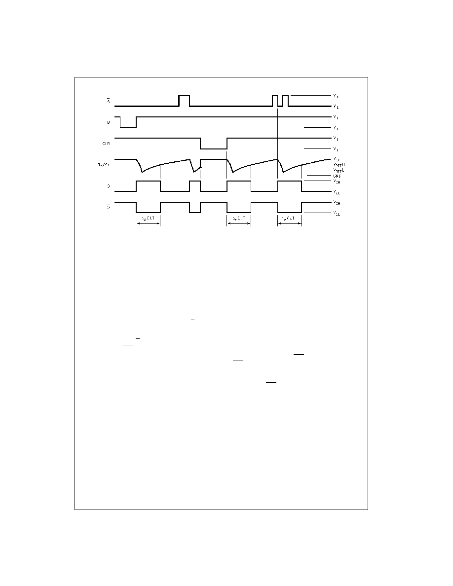
Timing Chart
Functional Description
1. Stand-by State
The external capacitor (Cx) is fully charged to V
CC
in
the Stand-by State. That means, before triggering, the
Q
P
and Q
N
transistors which are connected to the Rx/
Cx node are in the off state. Two comparators that
relate to the timing of the output pulse, and two refer-
ence voltage supplies turn off. The total supply current
is only leakage current.
2. Trigger Operation
Trigger operation is effective in any of the following
three cases. First, the condition where the A input is
LOW, and B input has a rising signal; second, where
the B input is HIGH, and the A input has a falling signal;
and third, where the A input is LOW and the B input is
HIGH, and the CLR input has a rising signal.
After a trigger becomes effective, comparators C1 and
C2 start operating, and Q
N
is turned on. The external
capacitor discharges through Q
N
. The voltage level at
the Rx/Cx node drops. If the Rx/Cx voltage level falls to
the internal reference voltage V
ref
L, the output of C1
becomes LOW. The flip-flop is then reset and Q
N
turns
off. At that moment C1 stops but C2 continues operat-
ing.
After Q
N
turns off, the voltage at the Rx/Cx node starts
rising at a rate determined by the time constant of
external capacitor Cx and resistor Rx.
Upon triggering, output Q becomes HIGH, following
some delay time of the internal F/F and gates. It stays
HIGH even if the voltage of Rx/Cx changes from falling
to rising. When Rx/Cx reaches the internal reference
voltage V
ref
H, the output of C2 becomes LOW, the out-
put Q goes LOW and C2 stops its operation. That
means, after triggering, when the voltage level of the
Rx/Cx node reaches V
ref
H, the IC returns to its
MONOSTABLE state.
With large values of Cx and Rx, and ignoring the dis-
charge time of the capacitor and internal delays of the
IC, the width of the output pulse, t
W
(OUT), is as fol-
lows:
t
W
(OUT)
=
1.0 Cx Rx
3. Reset Operation
In normal operation, the CLR input is held HIGH. If
CLR is LOW, a trigger has no affect because the Q out-
put is held LOW and the trigger control F/F is reset.
Also, Q
p
turns on and Cx is charged rapidly to V
CC
.
This means if CLR is set LOW, the IC goes into a wait
state.

www.fairchildsemi.com
4
7
4
VH
C22
1
A
Absolute Maximum Ratings
(Note 1)
Recommended Operating
Conditions
(Note 2)
Note 1: Absolute maximum ratings are values beyond which the device
may be damaged or have its useful life impaired. The databook specifica-
tions should be met, without exception, to ensure that the system design is
reliable over its power supply, temperature, and output/input loading vari-
ables. Fairchild does not recommended operation outside data book speci-
fications.
Note 2: Unused inputs must be used HIGH or LOW. They may not float.
Note 3: The maximum allowable values of Cx and Rx are a function of the
leakage of capacitor Cx, the leakage of the device, and leakage due to
board layout and surface resistance.
Susceptibility to externally induced noise signals may occur for Rx
>
1 M
.
DC Electrical Characteristics
Note 4: Per Circuit
Supply Voltage (V
CC
)
-
0.5V to
+
7.0V
DC Input Voltage (V
IN
)
-
0.5V to
+
7.0V
DC Output Voltage (V
OUT
)
-
0.5 to V
CC
+
0.5V
Input Diode Current (I
IK
)
-
20 mA
Output Diode Current (I
OK
)
±
20 mA
DC Output Current (I
OUT
)
±
25 mA
DC V
CC
/Current (I
CC
)
±
50 mA
Storage Temperature (T
STG
)
-
65
°
C to 150
°
C
Lead Temperature (T
L
)
Soldering, 10 seconds
260
°
C
Supply Voltage (V
CC
)
2.0V to
+
5.5V
Input Voltage (V
IN
)
0V to
+
5.5V
Output Voltage (V
OUT
)
0V to V
CC
Operating Temperature
(T
opr
)
-
40
°
to
+
85
°
C
Input Rise and Fall Time
(t
r
, t
f
) (CLR only)
V
CC
=
3.3V
±
0.3V
0
100 ns/V
V
CC
=
5.0V
±
0.5V
0
20 ns/V
External Capacitor - Cx
No Limitation (Note 3) F
External Resistor - Rx
>
5 k
(Note 3) (V
CC
=
2.0V)
>
1 k
(Note 3) (V
CC
>
3.0V)
Symbol
Parameter
V
CC
(V)
T
A
=
25
°
C
T
A
=
-
40
°
to 85
°
C
Units
Conditions
Min
Typ
Max
Min
Max
V
IH
HIGH Level
2.0
1.50
1.50
V
Input Voltage
3.0
-
5.5
0.7 V
CC
0.7 V
CC
V
IL
LOW Level
2.0
0.50
0.50
V
Input Voltage
3.0
-
5.5
0.3 V
CC
0.3 V
CC
V
OH
HIGH Level
2.0
1.9
2.0
1.9
V
IN
=
V
IH
I
OH
=
-
50
µ
A
Output Voltage
3.0
2.9
3.0
2.9
V
or V
IL
4.5
4.4
4.5
4.4
3.0
2.58
2.48
V
I
OH
=
-
4 mA
4.5
3.94
3.80
I
OH
=
-
8 mA
V
OL
LOW Level
2.0
0.0
0.1
0.1
V
V
IN
=
V
IH
I
OL
=
50
µ
A
Output Voltage
3.0
0.0
0.1
0.1
or V
IL
4.5
0.0
0.1
0.1
3.0
0.36
0.44
I
OL
=
4 mA
4.5
0.36
0.44
I
OL
=
8 mA
I
IN
Input Leakage Current
0
-
5.5
±
0.1
±
1.0
µ
A
V
IN
=
5.5V or GND
I
IN
Rx/Cx Terminal
5.5
±
0.25
±
2.50
µ
A
V
IN
=
V
CC
or GND
Off-State Current
I
CC
Quiescent Supply Current
5.5
4.0
40.0
µ
A
V
IN
=
V
CC
or GND
I
CC
Active--State (Note 4)
3.0
160
250
280
V
IN
=
V
CC
or GND
Supply Current
4.5
380
500
650
µ
A
Rx/Cx
=
0.5 V
CC
5.5
560
750
975

5
www.fairchildsemi.com
7
4
VH
C22
1
A
AC Electrical Characteristics
(Note 6)
Note 5: C
PD
is defined as the value of the internal equivalent capacitance which is calculated from the operating current consumption without load. Average
operating current can be obtained by the equation:
I
CC
(opr.)
=
C
PD
*V
CC
*f
IN
+
I
CC
1
*Duty/100
+
I
CC
/2 (per Circuit)
I
CC
1
: Active Supply Current
Duty: %
Note 6: Refer to 74VHC221A Timing Chart.
AC Operating Requirement
Symbol
Parameter
V
CC
(V)
T
A
=
25
°
C
T
A
=
-
40
°
C to
+
85
°
C
Units
Conditions
Min
Typ
Max
Min
Max
t
PLH
Propagation Delay Time
3.3
±
0.3
13.4
20.6
1.0
24.0
ns
C
L
=
15 pF
t
PHL
(A, BQ, Q)
15.9
24.1
1.0
27.5
C
L
=
50 pF
5.0
±
0.5
8.1
12.0
1.0
14.0
ns
C
L
=
15 pF
9.6
14.0
1.0
16.0
C
L
=
50 pF
t
PLH
Propagation Delay Time
3.3
±
0.3
14.5
22.4
1.0
26.0
ns
C
L
=
15 pF
t
PHL
(CLR Trigger--Q, Q)
17.0
25.9
1.0
29.5
C
L
=
50 pF
5.0
±
0.5
8.7
12.9
1.0
15.0
ns
C
L
=
15 pF
10.2
14.9
1.0
17.0
C
L
=
50 pF
t
PLH
Propagation Delay Time
3.3
±
0.3
10.3
15.8
1.0
18.5
ns
C
L
=
15 pF
t
PHL
(CLR--Q, Q)
12.8
19.3
1.0
22.0
C
L
=
50 pF
5.0
±
0.5
6.3
9.4
1.0
11.0
ns
C
L
=
15 pF
7.8
11.4
1.0
13.0
C
L
=
50 pF
t
WOUT
Output Pulse Width
2.0
415
C
X
=
28 pF
3.3
±
0.3
345
ns
C
L
=
50 pF R
X
=
6 k
5.0
±
0.5
312
3.3
±
0.3
160
240
300
ns
C
L
=
50 pF Cx
=
28 pF
5.0
±
0.5
133
200
240
Rx
=
2 k
3.3
±
0.3
90
100
110
90
110
µ
s
C
L
=
50 pF Cx
=
0.01
µ
F
5.0
±
0.5
90
100
110
90
110
Rx
=
10 k
3.3
±
0.3
0.9
1.0
1.1
0.9
1.1
ms
C
L
=
50 pF Cx
=
0.1
µ
F
5.0
±
0.5
0.9
1.0
1.1
0.9
1.1
Rx
=
10 k
t
wOUT
Output Pulse Width Error
Between Circuits
±
1
%
(In same Package)
C
IN
Input Capacitance
4
10
10
pF
V
CC
=
Open
C
PD
Power Dissipation
73
pF
(Note 5)
Capacitance
Symbol
Parameter
V
CC
(V)
T
A
=
25
°
C
T
A
=
-
40
°
C to
+
85
°
C
Units
Min
Typ
Max
Min
Max
t
W
(L)
Minimum Trigger
3.3
5.0
5.0
ns
t
W
(H)
Pulse Width
5.0
5.0
5.0
t
W
(L)
Minimum Clear
3.3
5.0
5.0
ns
Pulse Width
5.0
5.0
5.0