Äîêóìåíòàöèÿ è îïèñàíèÿ www.docs.chipfind.ru
XR88C681
�
�
FEATURES
!" #
$
$
%
%&
'
% '(
$
%(
)$*++$ '(%
$ *++$
%(%
,- *(% (
./ *( #
'
%
#
*( 0
% (
1 *(
%
#
$
$
*( '(
+ 2'
%(
$ '(
2!
'3 ((&
!( *( 4 5 '3 .%" /5 '3
63.%
7"
�28" 9' 9,*
:
$
9,*
: $%
(+
'(
/ *(
.(
#
( 2(- %3 #
$((
%
#
;'
'3
$- < ,(
#,
$ << ,(
,9 ,'3-%
&
,- #
(%& (
= 0
,% % < ,(
#,
$ << ,(
,9 ,'3-%
&
> 0
,% #
% (
- + %
'%
#
% < ,(
#,
$ << ,(
,9
,'3-%
&
( $ ( ( =6 7(
*(
$
( %'( + &%
$& $ $' (
- ,
( ( /=
$
(-
('% / $('%
$
'$ 9 , '
-&
APPLICATIONS
($( &%%
( ,., (
2 + $
('(
&%%
GENERAL DESCRIPTION
25
�
(%
%&
'
% '(
$
%( �
(% $ '
('(
% $('
($% +& (
$
$
+ $! %&
'
%
'
('(
'
% (
%(
- '3- �
(% $%(-
$ + % (
(''%% %$ %&%%
$
& %$ (
$ (
$(
(
5==/= $(' ++% %(
- # %(
+
==.=6" ==/.==" ?=" ?=" /=!!
$ /6!!
(''%% +((%
�
(% +('$ %(
- $
'$ & "
( (- +
' $
%(& 2,#. =
·
'%%
($ (- +
'
$ '
%(
"
$ (% '3-$ (
< (
,#," = (
,#,"
$ <<
(
,9
ORDERING INFORMATION
Part No.
Pin Package
Operating
Temperature Range
5==/=@
<< ,9
>
5==/=7.<
< #,
>
5==/=,.=
= ,#,
>
5==/=,.<
< ,#,
>
5==/=@
<< ,9
< A=6
5==/=7.<
< #,
< A=6
5==/=,.=
= ,#,
< A=6
5==/=,.<
< ,#,
< A=6
XR88C681
$ '$
*(
0
5
5
#
*%
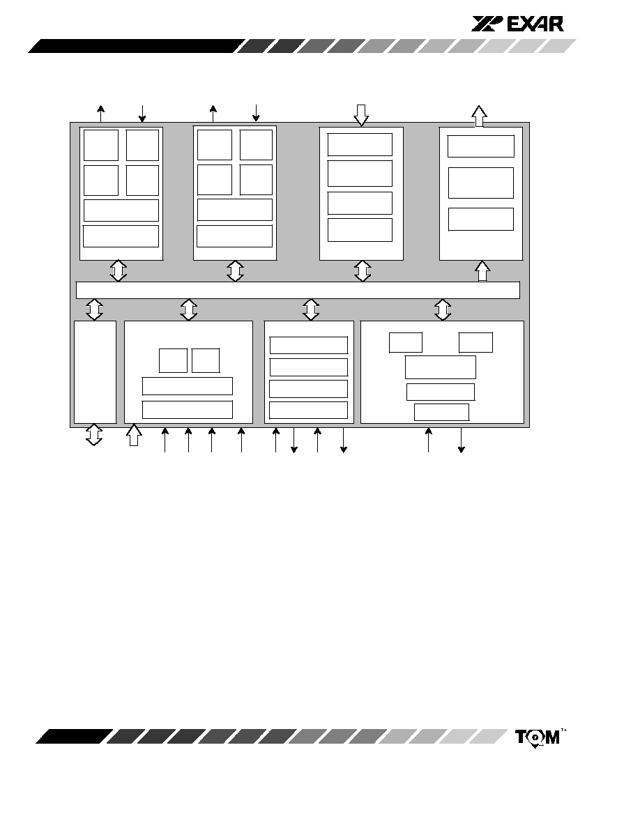
Figure 1. Block Diagram of the XR88C681
$$%% '$
*
(
#
#
#
#
#;
*
.(
((
-
*%
*++
>
1
B 22
#2# #2 #
: #7
5.9:
5
- +
'%
#,
#,
#
,
#, #,/
8
8
$ -(%%
% -(%
*
5*
5*
8
8
$ -(%%
% -(%
,
,
'(
'
9-('
,
,
, ,>
%'(
XR88C681
1
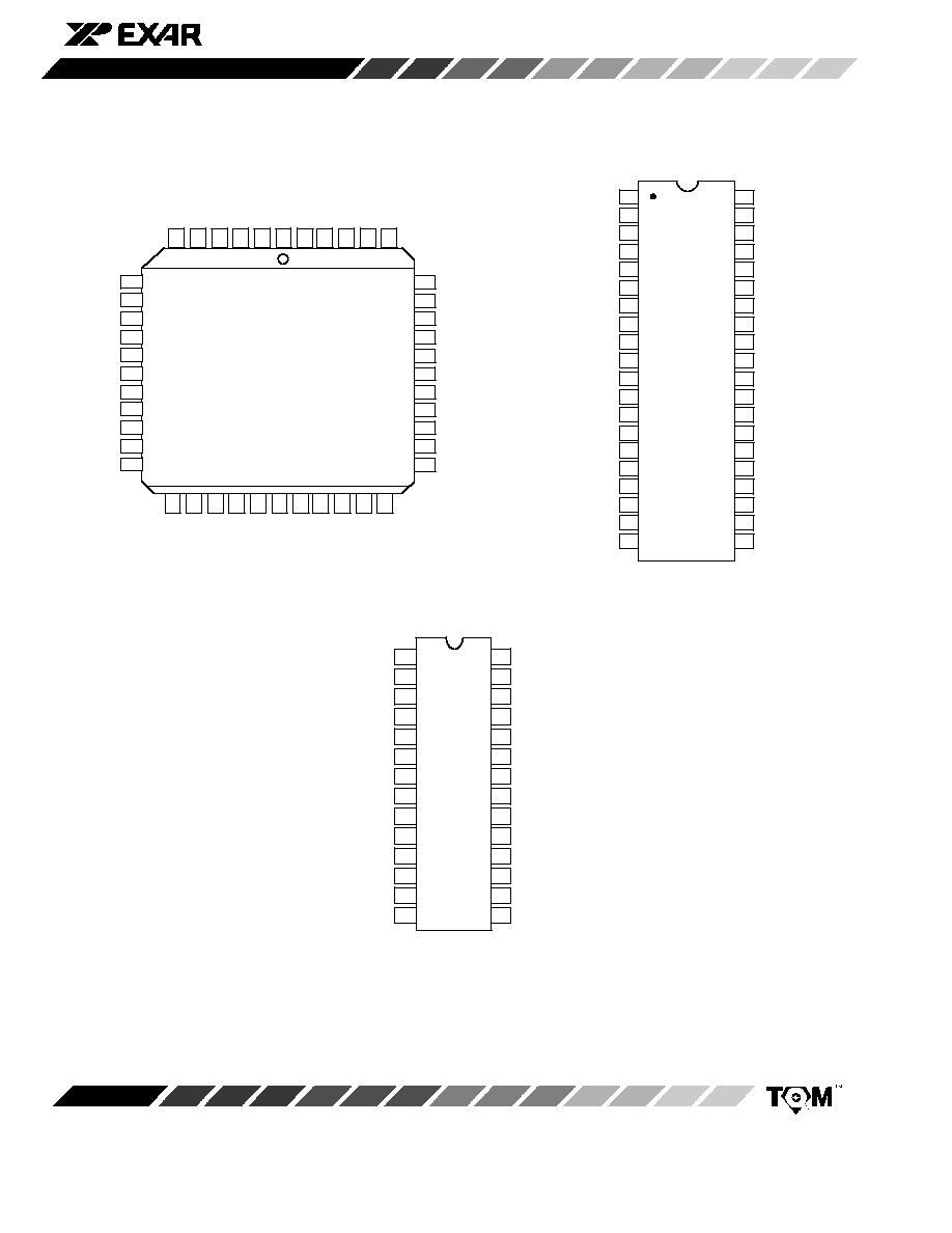
PIN CONFIGURATION
;
#,
22
5
5.9:
5
5
7
1
/
1
<
B
6
5*
5*
,
,
1
<
6
/
>
#7
07
28 Lead PDIP (0.600")
1
<
6
/
>
=
=
>
/
6
<
1
=
>
6
/
>
=
/
6
<
1
1
<
6
/
>
=
<
1
1=
1>
1/
16
1<
11
1
1
1
<
1
=
>
40 Lead PDIP, CDIP (0.600")
<
/
#7
,/
,
,
,<
5.9:
5
5
5
#,
22
#,<.#2#
#,6.#2
#,/.#
:
;
6
>
07
,>
1
,
,1
,6
5*
5*
B
1
#,
#,1
#,
XR-68C681CJ
PLCC
22
5
5.9:
5
7
5
,
,
,<
,6
,1
,
5*
7
5*
B
#,
1
44 Lead PLCC
,>
,/
#,
#,1
7
;''
#,<.#2#
#,6.#2
#,/.#
:
#,
1
6
>
07
7
#7
<
/
1
1=
1>
1/
16
1<
11
1
1
1
>
=
1
<
6
/
>
=
1
<
6
/
>
=
1
<
6
/
<<
<1
<
<
<
XR88C681
<
PIN DESCRIPTION
44 PLCC/
LCC
40 DIP,
CDP
28 DIP,
CDIP
Symbol
Type
Description
7
No Connection.
#
LSB of Address Input.
(% (
"
- (
$$%% #
%"
1 %$ %' '(
-(%% ((
�
$('" $(
- 2
$ B#2 (
% ( ,�
1
#,1
5
#
5
?
#
Input Port 3.
0
,% #
B
�
(%
(
- (
#$" (% (
'
% %$ %
!
''3 (
+
%( 5
B
�
(% (
- (
?$" (% (
'
%$ % !
''3 (
+
'(
5
<
1
#
Address Input.
6
<
#,
*
#
Input Port 1.
0
,% #
(% (
'
%
%$ %
'( 9" C
*
$D (
*
/
6
1
#
Address Input.
>
/
<
1
#
MSB of Address Input.
(% (
"
- (
$$%% #
%"
%$ %' '(
-(%% ((
�
$('" $(
- 2
$ B#2 (
% (
,�
=
>
#,
#
Input 0.
0
,% #
(% (
'
% %$
% '(" C
$D (
=
6
B
#
Write Strobe (Active-Low).
CD
(% (
( (%
% CD (% '
% + *% (
$
$%%$ -(%" ((
�
%+ ''%
(%(
- $- + B
/
#
Read Strobe (Active Low).
CD
(% (
(
(%
% CD '% '
% + $$%%$ �
-(%
"
$ %
>
5*
#
Receive Serial Data Input (Channel B).
% %(-
(+('
( + '' (% '($ +(% #+ !
'( ''3"
5*" (% %'(+($" $ (% %$
(%(
- $- +
(% ''3
7
No Connect.
1
=
5*
Transmitter Serial Data Output (Channel B).
% %(-
(+('
( + '' (%
%($ +(% (% (%
$ (
(- 3(
- %
%( (% ($"
$(%$"
'
(% (
- (
' 9,
*
: $ #+
!
%( ''3 (% %'(+($"
5*"
%($ $ (% %(+$ +
%
( (+ -(%
+(
- $- + (% ''3
XR88C681
6
44 PLCC/
LCC
40 DIP,
CDP
28 DIP,
CDIP
Symbol
Type
Description
<
,
*
Output 1 (General Purpose Output).
(% '
%
-$ +
'(
% '(" C
*
E%
$D *
6
1
,1
5*.5
5*.5
..G
Output 3 (General Purpose Output).
(% '
% -$ +
'(
%4 C
*
%
( 5 ''3D 5*.5" C
* '(
5 ''3D 5*.5"
$(
" '(
C
.( $&D ..G
/
<
,6
5G.
�99.*
Output 5 (General Purpose Output Pin).
(%
(
'
% -$ +
'(
%
$(
"
'("
* C'( $&D C'( #
D (
$(' 5G.*. �99.*
>
6
,>
5G.*
Output 7. (General Purpose Output Pin).
(%
(
'
% -$ +
'(
%
$(
"
'(" C
%( $&D (
$(' +
*
5G.*
=
/
#.
Bi-Directional Data Bus.
>
1
#.
Bi-Directional Data Bus.
=
6
#.
Bi-Directional Data Bus.
1
>
#.
MSB of the Eight Bit Bi-Directional Data Bus.
%+%
,�
$ �
3 ' (% %
'
%(%(
- + (
% > % (% (%$
(
(% C(-D" !' $(
-
#
: '&' (
?
$
<
07
,B
Signal Ground.
1
7
No Connect.
<
6
#7
Interrupt Request Output (Active Low, Open Drain).
#7 (% %%$
''
' +
+
'(H% %3 (
(
- '
$((
% (% %(-
(
(
%%$ - #
(' (
$
(
-$
' '
$((
% '%(
- #
E% %
((
$
6
/
/
#.
Bi-Directional Data Bus.
/
1
>
<
#.
Bi-Directional Data Bus.
>
<
=
#.
Bi-Directional Data Bus.
=
6
#.
LSB of the Eight Bit Bi-Directional Data Bus.
%+%
,�
$ �
3 ' (% %
% (% (%$
(
(% C(-D" !'
$(
-
#
: '&' (
?$
/
,/
5G.
Output 6 (General Purpose Output).
(% (
'
% -$ +
'(
%
$(
" '(
" C
%( $&D (
$(' +
5G.