Untitled Document
EXAR
Corporation 48720 Kato Road, Fremont CA, 94538
·
(510) 668-7000
·
FAX (510) 668-7017
·
www.exar.com
PRELIMINARY
XR17C158
PCI BUS OCTAL UART
MARCH 2000
REV. 1.0.1
GENERAL DESCRIPTION
The XR17C158
1
(158) is an octal Universal Asyn-
chronous Receiver and Transmitter (UART). The de-
vice is designed to meet the 32-bit PCI Bus and high
bandwidth requirement in communication systems.
The global interrupt source register provides a com-
plete interrupt status indication for all 8 channels to
speed up interrupt parsing. Each UART has its own
16C550 compatible set of configuration registers,
transmit and receive FIFOs of 64 bytes, fully pro-
grammable transmit and receive FIFO level triggers,
transmit and receive FIFO level counters, automatic
RTS/CTS or DTR/DSR hardware flow control with
programmable hysteresis, automatic software (Xon/
Xoff) flow control, IrDA (Infrared Data Association)
encoder/decoder, 8 multi-purpose definable inputs/
outputs, and a 16-bit general purpose timer/counter.
N
OTE
:
1 Covered by U.S. Patent #5,649,122 and #5,832,205
APPLICATIONS
· Remote Access Servers
· Ethernet Network to Serial Ports
· Network Management
· Factory Automation and Process Control
· Point-of-Sale Systems
· Multi-port RS-232/RS-422/RS-485 Cards
FEATURES
· High Performance Octal UART
· 32-bit PCI Bus Interface with EEPROM Interface
- Interrupt Source Register for all 8 UARTs
- Data Transfer in Byte, Word and Double-word
- Read/Write Burst Operation
· Each UART Includes
- 16C550 Compatible Registers
- 64-byte Transmit and Receive FIFOs
- Transmit and Receive FIFO Level Counters
- Automatic RTS/CTS or DTR/DSR Flow Control
- Automatic Xon/Xoff Software Flow Control
- RS485 Half-duplex Control with Selectable Delay
- Infrared (IrDA 1.0) Data Encoder/Decoder
- Programmable Data Rate with Prescaler
- Up to 6.25 Mbps Serial Data Rate
· Eight Multi-Purpose Inputs/outputs
· A General Purpose 16-bit Timer/Counter
· Sleep Mode with Automatic Wake-up
· 5V Operation (PCI Compliance)
· 3.3V Operation with 5V Tolerant Inputs
· 144-pin TQFP Package (20x20x1.4mm)
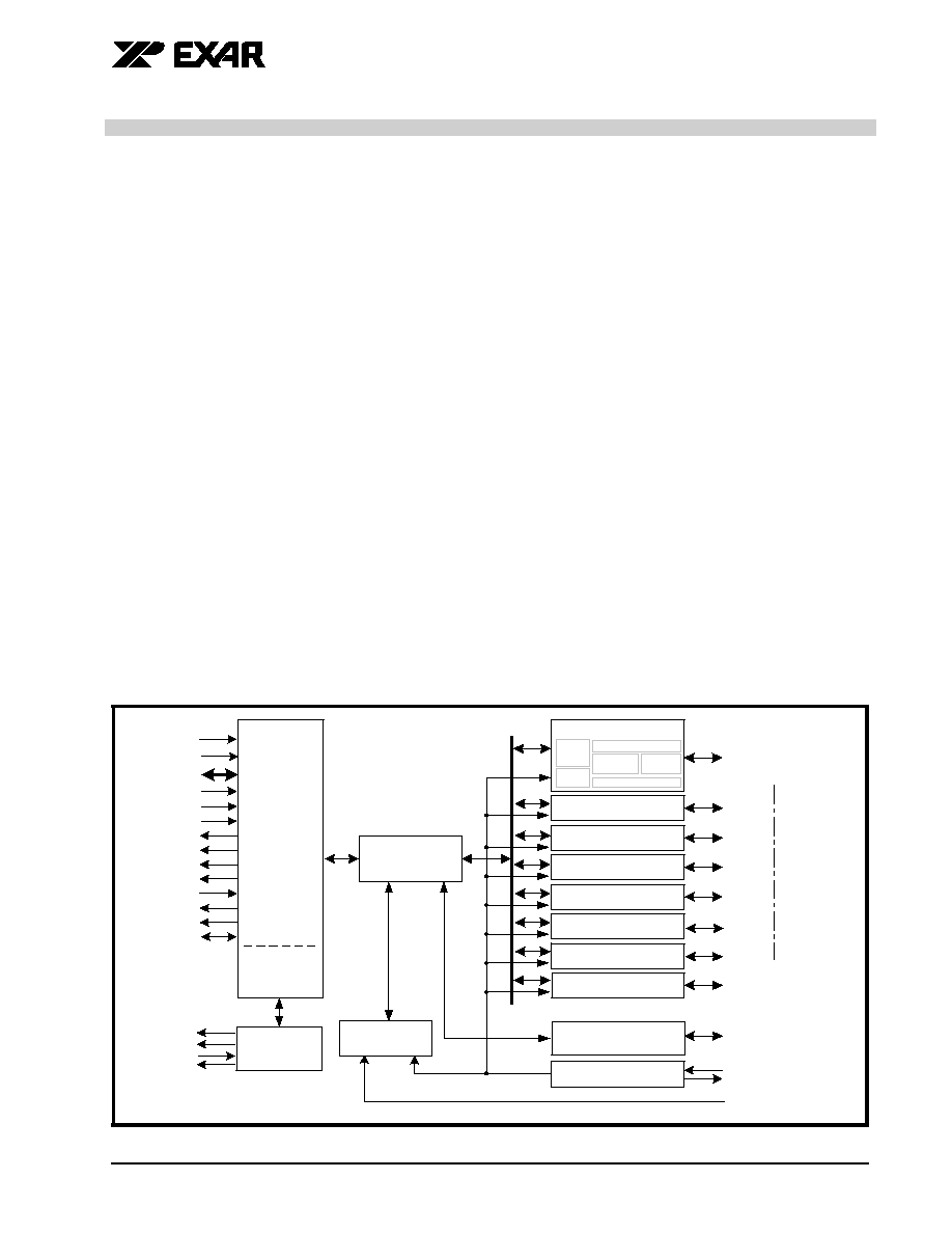
F
IGURE
1. B
LOCK
D
IAGRAM
TMRCK
Device
Configuration
Registers
XTAL1/CLK
XTAL2
Crystal Osc/Buffer
UART Channel 0
TX0, RX0, DTR0#,
DSR0#, RTS0#,
CTS0#, CD0#, RI0#
PCI Local
Bus
Interface
CLK
RST#
AD[31:0]
C/BE[3:0]#
PAR
FRAME#
IRDY#
TRDY#
DEVSEL#
STOP#
IDSEL
PERR#
SERR#
INTA#
Configuration
Space
Registers
.
MPIO0- MPIO7
Multi-purpose
Inputs/Outputs
TX7, RX7, DTR7#,
DSR7#, RTS7#,
CTS7#, CD7#, RI7#
UART Channel 7
UART Channel 6
UART Channel 5
UART Channel 4
UART Channel 3
UART Channel 2
UART Channel 1
16-bit
Timer/Counter
EECK
EEDI
EEDO
EECS
EEPROM
Interface
64 Byte TX FIFO
64 Byte RX FIFO
BRG
IR
ENDEC
TX & RX
UART
Regs
PCI BUS OCTAL UART
XR17C158
PRELIMINARY
REV. 1.0.0
2
F
IGURE
2. P
IN
O
UT
OF
THE
D
EVICE
RX
4
GN
D
MPIO5
GND
TMRCK
ENIR
XR17C158
108
107
106
105
104
103
102
101
100
99
98
97
96
95
94
93
92
91
90
89
88
87
86
85
84
83
82
81
80
79
MP
IO
0
MP
IO
1
VC
C
GN
D
CT
S
4
#
TX
5
1
2
3
4
5
6
7
8
9
10
11
12
13
14
15
16
17
18
19
20
21
22
23
24
25
26
27
28
29
30
AD
24
C
BE3
ID
SEL
VC
C
GN
D
AD
23
AD
22
AD
21
AD
20
AD
19
AD
18
AD
17
AD
16
C
BE2
F
R
AM
E#
I
RDY
#
T
RDY
#
D
EVSEL#
VC
C
ST
OP
#
P
E
RR#
S
E
RR#
PAR
C
BE1
AD
15
AD
14
AD
13
AD
12
AD
11
TX7
RX6
CTS6#
DSR6#
CD6#
RI6#
RTS6#
DTR6#
TX6
GND
VCC
MPIO7
MPIO6
MPIO4
RX5
CTS5#
53
54
55
56
57
58
59
60
61
62
63
64
65
66
67
68
69
70
71
72
RX1
CTS1#
DSR1#
CD1#
RI1#
RTS1#
DTR1#
TX1
EECS
EEDI
EECK
EEDO
VCC
TEST#
XTAL1
XTAL2
128
127
126
125
124
123
122
121
120
119
118
117
116
115
114
113
112
111
110
109
31
32
33
34
AD
10
AD
9
AD
8
VC
C
35
36
GN
D
C
BE0
MP
IO
2
78
77
76
75
74
73
DT
R5
#
RT
S
5
#
RI
5
#
CD5
#
MP
IO
3
RI7#
DTR7#
AD7
AD6
AD5
AD4
AD3
AD2
AD1
AD0
VCC
RX7
CTS7#
DSR7#
CD7#
RTS7#
37
38
39
40
41
42
43
44
45
46
47
48
49
50
51
52
AD26
AD27
AD28
AD29
AD30
AD31
VCC
GND
CLK
RST#
144
143
142
141
140
139
138
137
136
135
134
133
132
131
130
129
TX
4
DT
R4
#
RT
S
4
#
RI
4
#
CD4
#
RX
3
CT
S
3
#
TX
3
DT
R3
#
RT
S
3
#
RI
3
#
CD3
#
RX
2
CT
S
2
#
TX
2
DT
R2
#
RT
S
2
#
RI
2
#
CD2
#
DS
R2
#
DS
R3
#
DS
R4
#
DS
R5
#
RX0
CTS0#
DSR0#
CD0#
RI0#
RTS0#
DTR0#
TX0
INTA#
AD25
ORDERING INFORMATION
P
ART
N
UMBER
P
ACKAGE
O
PERATING
T
EMPERATURE
R
ANGR
XR17C158CV
144-TQFP
0°C to +70°C
XR17C158IV
144-TQFP
-40°C to +85°C
XR17C158
PCI BUS OCTAL UART
PRELIMINARY
REV. 1.0.0
3
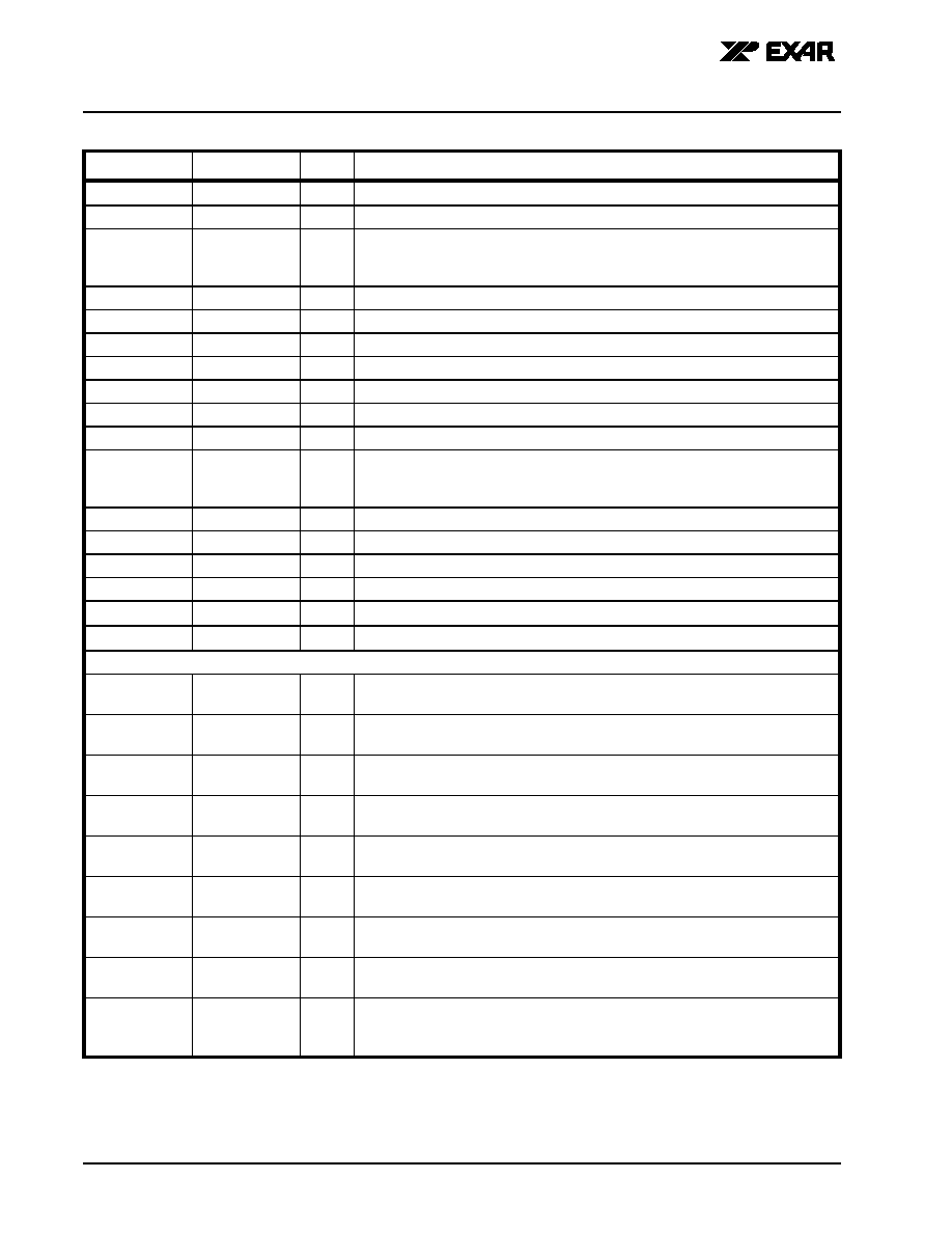
PIN DESCRIPTIONS
Pin Description
N
AME
P
IN
#
T
YPE
D
ESCRIPTION
PCI LOCAL BUS INTERFACE
RST#
134
I
Bus reset input (active low). It resets the PCI local bus configuration space
registers, device configuration registers and UART channel registers to the
default condition, see
Table 18
.
CLK
135
I
Bus clock input of up to 33MHz.
AD31-AD0
1
6-13
26-33
37-44
138-144
IO
Address data lines [31:0] (bidirectional).
FRAME#
15
I
Bus transaction cycle frame (active low). It indicates the begining and duration
of an access.
C/BE0#
-
C/BE3#
36,25,14,2
I
Bus Command/Byte Enable [3:0] (active low). This line is multiplexed for bus
Command during the address phase and Byte Enables during the data
phase.
IRDY#
16
I
Initiator Ready (active low). During a write, it indicates that valid data is
present on data bus. During a read, it indicates the master is ready to accept
data.
TRDY#
17
O
Target Ready (active low).
STOP#
21
O
Target request to stop current transaction (active low).
IDSEL
3
I
Initialization device select (active high).
DEVSEL#
18
O
Device select to the XR17C158 (active low).
INTA#
133
OD
Device interrupt from XR17C158 (open drain, active low).
PAR
24
IO
Parity is even across AD[31:0] and C/BE[3:0]#. (bidirectional, active high ).
PERR#
22
O
Parity error indicator to host, (active low). Optional in bus target application.
SERR#
23
OD
System error indicator to host (open drain, active low). Optional in bus target
application.
MODEM OR SERIAL I/O INTERFACE
TX0
125
O
UART channel 0 Transmit Data or infrared transmit data.
RX0
132
I
UART channel 0 Receive Data or infrared receive data. Normal RXD input
idles at logic 1 condition. The infrared pulses can be inverted internally prior
the decoder by FCTR[4].
RTS0#
127
O
UART channel 0 Request to Send or general purpose output (active low).
CTS0#
131
I
UART channel 0 Clear to Send or general purpose input (active low).
DTR0#
126
O
UART channel 0 Data Terminal Ready or general purpose output (active low).
DSR0#
130
I
UART channel 0 Data Set Ready or general purpose input (active low).
CD0#
129
I
UART channel 0 Carrier Detect or general purpose input (active low).
RI0#
128
I
UART channel 0 Ring Indicator or general purpose input (active low).
TX1
117
O
UART channel 1 Transmit Data or infrared transmit data.
RX1
124
I
UART channel 1 Receive Data or infrared receive data. Normal RXD input
idles at logic 1 condition. The infrared pulses can be inverted internally prior
the decoder by FCTR[4].
RTS1#
119
O
UART channel 1 Request to Send or general purpose output (active low).
CTS1#
123
I
UART channel 1 Clear to Send or general purpose input (active low).
PCI BUS OCTAL UART
XR17C158
PRELIMINARY
REV. 1.0.0
4
DTR1#
118
O
UART channel 1 Data Terminal Ready or general purpose output (active low).
DSR1#
122
I
UART channel 1 Data Set Ready or general purpose input (active low).
CD1#
121
I
UART channel 1
Carrier Detect or general purpose input (active low).
.
RI1#
120
I
UART channel 1 Ring Indicator or general purpose input (active low).
TX2
106
O
UART channel 2 Transmit Data or infrared transmit data.
RX2
99
I
UART channel 2 Receive Data or infrared receive data. Normal RXD input
idles at logic 1 condition. The infrared pulses can be inverted internally prior
the decoder by FCTR[4].
RTS2#
104
O
UART channel 2 Request to Send or general purpose output (active low).
CTS2#
100
I
UART channel 2 Clear to Send or general purpose input (active low).
DTR2#
105
O
UART channel 2 Data Terminal Ready or general purpose output (active low).
DSR2#
101
I
UART channel 2 Data Set Ready or general purpose input (active low).
CD2#
102
I
UART channel 2
Carrier Detect or general purpose input (active low).
RI2#
103
I
UART channel 2 Ring Indicator or general purpose intput (active low).
TX3
98
O
UART channel 3 Transmit Data or infrared transmit data.
RX3
91
I
UART channel 3 Receive Data or infrared receive data. Normal RXD input
idles at logic 1 condition. The infrared pulses can be inverted internally prior
the decoder by FCTR[4].
RTS3#
96
O
UART channel 3 Request to Send or general purpose output (active low).
CTS3#
92
I
UART channel 3 Clear to Send or general purpose input (active low).d.
DTR3#
97
O
UART channel 3 Data Terminal Ready or general purpose output (active low).
DSR3#
93
I
UART channel 3 Data Set Ready or general purpose input (active low).
CD3#
94
I
UART channel 3
Carrier Detect or general purpose input (active low).
RI3#
95
I
UART channel 3 Ring Indicator or general purpose input
(active low).
TX4
88
O
UART channel 4 Transmit Data or infrared transmit data.
RX4
81
I
UART channel 4 Receive Data or infrared receive data. Normal RXD input
idles at logic 1 condition. The infrared pulses can be inverted internally prior
the decoder by FCTR[4].
RTS4#
86
O
UART channel 4 Request to Send or general purpose output (active low).
CTS4#
82
I
UART channel 4 Clear to Send or general purpose input (active low).
DTR4#
87
O
UART channel 4 Data Terminal Ready or general purpose output (active low).
DSR4#
83
I
UART channel 4 Data Set Ready or general purpose input (active low).
CD4#
84
I
UART channel 4
Carrier Detect or general purpose input (active low).
RI4#
85
I
UART channel 4 Ring Indicator or general purpose input
(active low).
TX5
80
O
UART channel 5 Transmit Data or infrared transmit data.
RX5
71
I
UART channel 5 Receive Data or infrared receive data. Normal RXD input
idles at logic 1 condition. The infrared pulses can be inverted internally prior
the decoder by FCTR[4].
RTS5#
78
O
UART channel 5 Request to Send or general purpose output (active low).
CTS5#
72
I
UART channel 5 Clear to Send or general purpose input (active low).
DTR5#
79
O
UART channel 5 Data Terminal Ready or general purpose output (active low).
DSR5#
75
I
UART channel 5 Data Set Ready or general purpose input (active low).
CD5#
76
I
UART channel 5
Carrier Detect or general purpose input (active low).
Pin Description
N
AME
P
IN
#
T
YPE
D
ESCRIPTION
XR17C158
PCI BUS OCTAL UART
PRELIMINARY
REV. 1.0.0
5
RI5#
77
I
UART channel 5 Ring Indicator or general purpose
input (active low).
TX6
62
O
UART channel 6 Transmit Data or infrared transmit data.
RX6
55
I
UART channel 6 Receive Data or infrared receive data. Normal RXD input
idles at logic 1 condition. The infrared pulses can be inverted internally prior
the decoder by FCTR[4].
RTS6#
60
O
UART channel 6 Request to Send or general purpose output (active low).
CTS6#
56
I
UART channel 6 Clear to Send or general purpose input (active low).
DTR6#
61
O
UART channel 6 Data Terminal Ready or general purpose output (active low).
DSR6#
57
I
UART channel 6 Data Set Ready or general purpose input (active low).
CD6#
58
I
UART channel 6 Carrier Detect or general purpose input (active low).
RI6#
59
I
UART channel 6 Ring Indicator or general purpose input (active low).
TX7
54
O
UART channel 7 Transmit Data or infrared transmit data.
RX7
47
I
UART channel 7 Receive Data or infrared receive data. Normal RXD input
idles at logic 1 condition. The infrared pulses can be inverted internally prior
the decoder by FCTR[4].
RTS7#
52
O
UART channel 7 Request to Send or general purpose output (active low).
CTS7#
48
I
UART channel 7 Clear to Send or general purpose input (active low).
DTR7#
53
O
UART channel 7 Data Terminal Ready or general purpose output (active low)..
DSR7#
49
I
UART channel 7 Data Set Ready or general purpose input (active low).
CD7#
50
I
UART channel 7
Carrier Detect or general purpose input (active low).
RI7#
51
I
UART channel 7 Ring Indicator or general purpose
input (active low).
ANCILLARY SIGNALS
MPIO0
108
I/O
Multi-purpose input/output 0. The function of this pin is defined thru the Con-
figuration Register MPIOSEL, MPIOLVL, MPIOINV, MPIO3T and MPIOINT
MPIO1
107
I/O
Multi-purpose input/output 1. The function of this pin is defined thru the Con-
figuration Register MPIOSEL, MPIOLVL, MPIOINV, MPIO3T and MPIOINT.
MPIO2
74
I/O
Multi-purpose input/output 2. The function of this pin is defined thru the Con-
figuration Register MPIOSEL, MPIOLVL, MPIOINV, MPIO3T and MPIOINT.
MPIO3
73
I/O
Multi-purpose input/output 3. The function of this pin is defined thru the Con-
figuration Register MPIOSEL, MPIOLVL, MPIOINV, MPIO3T and MPIOINT.
MPIO4
68
I/O
Multi-purpose input/output 4. The function of this pin is defined thru the Con-
figuration Register MPIOSEL, MPIOLVL, MPIOINV, MPIO3T and MPIOINT.
MPIO5
67
I/O
Multi-purpose input/output 5. The function of this pin is defined thru the Con-
figuration Register MPIOSEL, MPIOLVL, MPIOINV, MPIO3T and MPIOINT.
MPIO6
66
I/O
Multi-purpose input/output 6. The function of this pin is defined thru the Con-
figuration Register MPIOSEL, MPIOLVL, MPIOINV, MPIO3T and MPIOINT.
MPIO7
65
I/O
Multi-purpose input/output 7. The function of this pin is defined thru the Con-
figuration Register MPIOSEL, MPIOLVL, MPIOINV, MPIO3T and MPIOINT.
EECK
116
O
Serial clock to EEPROM.
An internal clock of CLK divide by 256 is used for
reading the vendor and su-vendor ID during power up or reset. However, it
can be manually clocked thru the Configuration Register REGB.
Pin Description
N
AME
P
IN
#
T
YPE
D
ESCRIPTION
Document Outline