Äîêóìåíòàöèÿ è îïèñàíèÿ www.docs.chipfind.ru
EXAR Corporation 48720 Kato Road, Fremont CA, 94538 · (510) 668-7000 · FAX (510) 668-7017 · www.exar.com · uarttechsupport@exar.com
áç
áç
áç
áç
XR16L788
HIGH PERFORMANCE OCTAL UART
SEPTEMBER 2001
REV. 1.1.4
GENERAL DESCRIPTION
The XR16L788
1
(788), formerly XR16L758, is a 5V
and 3.3V with 5V tolerant inputs octal Universal Asyn-
chronous Receiver and Transmitter (UART). The
highly integrated device is designed for high band-
width requirement in communication systems. A new
feature increases device driver efficiency includes a
global interrupt pin with global interrupt source regis-
ters that provide complete and detailed interrupt sta-
tus information for all 8 channels that will speed up in-
terrupt parsing. Other new facilities include simulta-
neous UART registers initialization, individual UART
channel soft-reset, DTR/DSR hardware flow control,
software flow control (Xoff/Xon) detection indicators,
RS-485 half-duplex direction control with programma-
ble turn-around delay, Intel or Motorola bus interface
and sleep mode now has a wake-up indicator.
N
OTE
:
Covered by US patents #5,649,122 and #5,949,787
APPLICATIONS
· Remote Access Servers
· Ethernet Network to Serial Ports
· Network Management
· Factory Automation and Process Control
· Point-of-Sale Systems
· Multi-port RS-232/RS-422/RS-485 Cards
NEW FEATURES:
· 5V and 3.3V with 5V Tolerant Inputs Operation
· Single Interrupt Output for all 8 UARTs
· Global Interrupt Source for all 8 UARTs
· 5G "Flat" UART Registers for Configurations
· Simultaneous UART Channels Initialization
· Auto RS485 Half-duplex Control with Program-
mable Turn-around Delay
· A General Purpose 16-bit Timer/Counter
· Sleep Mode with Wake-up Indication
· Highly Integrated Device for Space Saving
· First eight registers are 16C550 compatible
· 64-byte Transmit and Receive FIFOs
· Transmit and Receive FIFO Level Counters
· Programmable TX and RX FIFO Trigger Levels
· Automatic RTS/CTS or DTR/DSR Flow Control
· Selectable Hardware Flow Control Hysteresis
· Automatic Xon/Xoff Software Flow Control with Sta-
tus Indicator
· Infrared (IrDA 1.0) Data Encoder/Decoder
· Programmable Data Rate with Prescaler
· Up to 6.25 Mbps Serial Data Rate at 5V
· 100-pin QFP Package (14x20x3 mm)
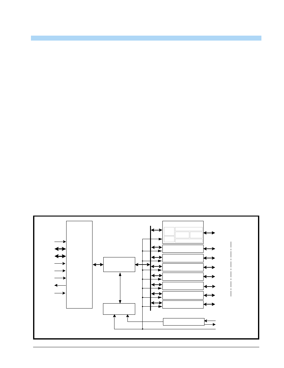
F
IGURE
1. B
LOCK
D
IAGRAM
T M R C K
D e vice
C o n figu ra tio n
R e g isters
X T A L1
X T A L2
C rystal O sc/B u ffer
U A R T C ha n ne l 0
T X 0 , R X 0 , D T R 0# ,
D S R 0# , R T S 0# ,
C T S 0 # , C D 0 #, R I0 #
D a ta B u s
Inte rfa ce
R S T #
A 7:A 0
IO R #
IO W #
C S #
IN T #
T X 7 , R X 7 , D T R 7# ,
D S R 7# , R T S 7# ,
C T S 7 # , C D 7 #, R I7 #
U A R T C ha n ne l 7
U A R T C ha n ne l 6
U A R T C ha n ne l 5
U A R T C ha n ne l 4
U A R T C ha n ne l 3
U A R T C ha n ne l 2
U A R T C ha n ne l 1
1 6-bit
T im e r/C o un ter
64 B yte T X FIF O
64 B yte R X F IF O
B R G
IR
E N D E C
T X & R X
U A R T
R eg s
D 7 :D 0
1 6/6 8#
áçýýýýýýýýýýýý
áçýýýýýýýýýýýý
áçýýýýýýýýýýýý
áçýýýýýýýýýýýý
XR16L788 OCTAL UART
REV. 1.1.4
2
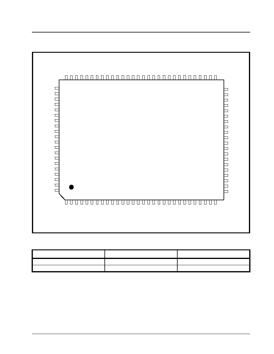
F
IGURE
2. P
IN
O
UT
OF
THE
D
EVICE
R
ST#
16/
68#
VC
C
GND
D7
D6
D5
D4
D3
D2
D1
D0
IO
W
#
T
M
RCK
EN
I
R
CS
#
IN
T
#
VC
C
GND
IO
R
#
A7
A6
A5
A4
A3
A2
A1
A0
VC
C
GND
2
4 5 6 7
9
8
3
1
1 0 1 1
1 3
1 2
1 4 1 5 1 6 1 7 1 8 1 9 2 0 2 1 2 2 2 3 2 4 2 5 2 6 2 7 2 8 2 9 3 0
7 1 7 0
6 8
6 9
6 7 6 6 6 5 6 4 6 3 6 2 6 1 6 0 5 9 5 8 5 7 5 6 5 5 5 4 5 3 5 2 5 1
81
82
84
83
85
86
87
88
89
90
91
92
93
94
95
96
97
98
99
1
0
0
X R 1 6 L 7 8 8
1 0 0 -Q F P
R X 7
TX4
DT
R4
#
R
TS4#
RI
4#
CD4
#
DS
R4
#
C
TS4#
RX
4
TX5
DT
R5
#
R
TS5#
RI
5#
CD5
#
DS
R5
#
7 2
7 3
7 4
7 5
7 6
7 7
7 8
8 0 7 9
C T S 7 #
D S R 7 #
C D 7 #
R I7#
R T S 7 #
D T R 7 #
T X 7
R X 6
C T S 6 #
D S R 6 #
C D 6 #
R I6#
R T S 6 #
D T R 6 #
T X 6
G N D
V C C
R X 5
C T S 5 #
TX3
DT
R3
#
R
TS3#
RI
3#
CD3
#
DS
R3
#
C
TS3#
RX
3
TX2
DT
R2
#
R
TS2#
RI
2#
CD2
#
DS
R2
#
C
TS2#
RX
2
R X 0
C T S 0 #
D S R 0 #
C D 0 #
R I0#
R T S 0 #
D T R 0 #
T X 0
R X 1
C T S 1 #
D S R 1 #
C D 1 #
R I1#
R T S 1 #
D T R 1 #
T X 1
V C C
G N D
X T A L 1
X T A L 2
31
32
34
33
35
36
37
38
39
40
41
42
43
44
45
46
47
48
49
50
ORDERING INFORMATION
P
ART
N
UMBER
P
ACKAGE
O
PERATING
T
EMPERATURE
R
ANGE
XR16L788CQ
14x20x3mm 100-QFP
0°C to +70°C
XR16L788IQ
14x20x3mm 100-QFP
-40°C to +85°C
XR16L788 OCTAL UART
áç
áç
áç
áç
REV. 1.1.4
3
PIN DESCRIPTIONS
N
AME
P
IN
#
T
YPE
D
ESCRIPTION
DATA BUS INTERFACE
A7-A0
20-27
I
Address data lines [7:0]. A0:A3 selects individual UART's 16 configuration reg-
isters, A4:A6 selects UART channel 0 to7, and A7 selects the global device
configuration registers.
D7:D0
5-12
IO
Data bus lines (7:0] (bidirectional).
IOR#
19
I
When 16/68# pin is at logic 1, it selects Intel bus interface and this input is
read strobe (active low). The falling edge instigates an internal read cycle and
retrieves the data byte from an internal register pointed by the address lines
[A7:A0], places it on the data bus to allow the host processor to read it on the
leading edge.
When 16/68# pin is at logic 0, it selects Motorola bus interface and this input
should be connected to VCC.
IOW#
13
I
When 16/68# pin is at logic 1, it selects Intel bus interface and this input
becomes write strobe (active low). The falling edge instigates the internal
write cycle and the leading edge transfers the data byte on the data bus to an
internal register pointed by the address lines.
When 16/68# pin is at logic 0, it selects Motorola bus interface and this input
becomes read (logic 1) and write (logic 0) signal (R/W#).
CS#
30
I
When 16/68# pin is at logic 1, this input is chip select (active low) to enable
the XR16L788 device.
When 16/68# pin is at logic 0, this input becomes the read and write strobe
(active low) for the Motorola bus interface.
INT#
16
OD
Global interrupt output from XR16L788 (open drain, active low). This output
requires an external pull-up resistor (47K-100K ohms) to operate properly. It
may be shared with other devices in the system to form a single interrupt line
to the host processor and have the software driver polls each device for the
interrupt status.
MODEM OR SERIAL I/O INTERFACE
TX0
93
O
UART channel 0 Transmit Data or infrared transmit data.
RX0
100
I
UART channel 0 Receive Data or infrared receive data. Normal RXD input
idles at logic 1 condition. The infrared pulses can be inverted internally prior
the decoder by FCTR[4].
RTS0#
95
O
UART channel 0 Request to Send or general purpose output (active low).
This port may be used for one of two functions:
1) auto hardware flow control, see EFR bit-6, MCR bits-1 & 2, FCTR bits 0-3
and IER bit-6
2) RS485 half-duplex direction control, see FCTR bit-5, MCR bit-2 and MSR
bits 4-7.
CTS0#
99
I
UART channel 0 Clear to Send or general purpose input (active low). It can be
used for auto hardware flow control, see EFR bit-7, MCR bit-2 and IER bit-7.
DTR0#
94
O
UART channel 0 Data Terminal Ready or general purpose output (active low).
This port may be used one of two functions.
1) auto hardware flow control, see EFR bit-6, FCTR bits-0 to 3, MCR bits-0 &
2, and IER bit-6
2) RS485 half-duplex direction control, see FCTR bit-5, MCR bit-2 and MSR
bit 4-7.
DSR0#
98
I
UART channel 0 Data Set Ready or general purpose input (active low). It can
be used for auto hardware flow control, see EFR bit-7, MCR bit-2 and IER bit-
7.
CD0#
97
I
UART channel 0 Carrier Detect or general purpose input (active low).

áçýýýýýýýýýýýý
áçýýýýýýýýýýýý
áçýýýýýýýýýýýý
áçýýýýýýýýýýýý
XR16L788 OCTAL UART
REV. 1.1.4
4
RI0#
96
I
UART channel 0 Ring Indicator or general purpose input (active low).
TX1
85
O
UART channel 1 Transmit Data or infrared transmit data.
RX1
92
I
UART channel 1 Receive Data or infrared receive data. Normal RXD input
idles at logic 1 condition. The infrared pulses can be inverted internally prior
the decoder by FCTR[4].
RTS1#
87
O
UART channel 1 Request to Send or general purpose output (active low). See
description of RTS0# pin.
CTS1#
91
I
UART channel 1 Clear to Send or general purpose input (active low). See
description of CTS0# pin.
DTR1#
86
O
UART channel 1 Data Terminal Ready or general purpose output (active low).
See description of DTR0# pin.
DSR1#
90
I
UART channel 1 Data Set Ready or general purpose input (active low). See
description of DSR0# pin.
CD1#
89
I
UART channel 1 Carrier Detect or general purpose input (active low).
RI1#
88
I
UART channel 1 Ring Indicator or general purpose input (active low).
TX2
80
O
UART channel 2 Transmit Data or infrared transmit data.
RX2
73
I
UART channel 2 Receive Data or infrared receive data. Normal RXD input
idles at logic 1 condition. The infrared pulses can be inverted internally prior
the decoder by FCTR[4].
RTS2#
78
O
UART channel 2 Request to Send or general purpose output (active low). See
description of RTS0# pin.
CTS2#
74
I
UART channel 2 Clear to Send or general purpose input (active low). See
description of CTS0# pin.
DTR2#
79
O
UART channel 2 Data Terminal Ready or general purpose output (active low).
See description of DTR0# pin.
DSR2#
75
I
UART channel 2 Data Set Ready or general purpose input (active low). See
description of DSR0# pin.
CD2#
76
I
UART channel 2 Carrier Detect or general purpose input (active low).
RI2#
77
I
UART channel 2 Ring Indicator or general purpose input (active low).
TX3
72
O
UART channel 3 Transmit Data or infrared transmit data.
RX3
65
I
UART channel 3 Receive Data or infrared receive data. Normal RXD input
idles at logic 1 condition. The infrared pulses can be inverted internally prior
the decoder by FCTR[4].
RTS3#
70
O
UART channel 3 Request to Send or general purpose output (active low). See
description of RTS0# pin.
CTS3#
66
I
UART channel 3 Clear to Send or general purpose input (active low). See
description of CTS0# pin.
DTR3#
71
O
UART channel 3 Data Terminal Ready or general purpose output (active low).
See description of DTR0# pin.
DSR3#
67
I
UART channel 3 Data Set Ready or general purpose input (active low). See
description of DSR0# pin.
CD3#
68
I
UART channel 3 Carrier Detect or general purpose input (active low).
RI3#
69
I
UART channel 3 Ring Indicator or general purpose input (active low).
TX4
64
O
UART channel 4 Transmit Data or infrared transmit data.
RX4
57
I
UART channel 4 Receive Data or infrared receive data. Normal RXD input
idles at logic 1 condition. The infrared pulses can be inverted internally prior
the decoder by FCTR[4].
N
AME
P
IN
#
T
YPE
D
ESCRIPTION
XR16L788 OCTAL UART
áç
áç
áç
áç
REV. 1.1.4
5
RTS4#
62
O
UART channel 4 Request to Send or general purpose output (active low). See
description of RTS0# pin.
CTS4#
58
I
UART channel 4 Clear to Send or general purpose input (active low). See
description of CTS0# pin.
DTR4#
63
O
UART channel 4 Data Terminal Ready or general purpose output (active low).
See description of DTR0# pin.
DSR4#
59
I
UART channel 4 Data Set Ready or general purpose input (active low). See
description of DSR0# pin.
CD4#
60
I
UART channel 4 Carrier Detect or general purpose input (active low).
RI4#
61
I
UART channel 4 Ring Indicator or general purpose input (active low).
TX5
56
O
UART channel 5 Transmit Data or infrared transmit data.
RX5
49
I
UART channel 5 Receive Data or infrared receive data. Normal RXD input
idles at logic 1 condition. The infrared pulses can be inverted internally prior
the decoder by FCTR[4].
RTS5#
54
O
UART channel 5 Request to Send or general purpose output (active low). See
description of RTS0# pin.
CTS5#
50
I
UART channel 5 Clear to Send or general purpose input (active low). See
description of CTS0# pin.
DTR5#
55
O
UART channel 5 Data Terminal Ready or general purpose output (active low).
See description of DTR0# pin.
DSR5#
51
I
UART channel 5 Data Set Ready or general purpose input (active low). See
description of DSR0# pin.
CD5#
52
I
UART channel 5 Carrier Detect or general purpose input (active low).
RI5#
53
I
UART channel 5 Ring Indicator or general purpose input (active low).
TX6
46
O
UART channel 6 Transmit Data or infrared transmit data.
RX6
39
I
UART channel 6 Receive Data or infrared receive data. Normal RXD input
idles at logic 1 condition. The infrared pulses can be inverted internally prior
the decoder by FCTR[4].
RTS6#
44
O
UART channel 6 Request to Send or general purpose output (active low). See
description of RTS0# pin.
CTS6#
40
I
UART channel 6 Clear to Send or general purpose input (active low). See
description of CTS0# pin.
DTR6#
45
O
UART channel 6 Data Terminal Ready or general purpose output (active low).
See description of DTR0# pin.
DSR6#
41
I
UART channel 6 Data Set Ready or general purpose input (active low). See
description of DSR0# pin.
CD6#
42
I
UART channel 6 Carrier Detect or general purpose input (active low).
RI6#
43
I
UART channel 6 Ring Indicator or general purpose input (active low).
TX7
38
O
UART channel 7 Transmit Data or infrared transmit data.
RX7
31
I
UART channel 7 Receive Data or infrared receive data. Normal RXD input
idles at logic 1 condition. The infrared pulses can be inverted internally prior
the decoder by FCTR[4].
RTS7#
36
O
UART channel 7 Request to Send or general purpose output (active low). See
description of RTS0# pin.
CTS7#
32
I
UART channel 7 Clear to Send or general purpose input (active low). See
description of CTS0# pin.
DTR7#
37
O
UART channel 7 Data Terminal Ready or general purpose output (active low).
See description of DTR0# pin.
N
AME
P
IN
#
T
YPE
D
ESCRIPTION
Document Outline