Äîêóìåíòàöèÿ è îïèñàíèÿ www.docs.chipfind.ru
Exar
Corporation 48720 Kato Road, Fremont CA, 94538
·
(510) 668-7000
·
FAX (510) 668-7017
·
www.exar.com
xr
XR16L2450
2.25V TO 5.5V DUART
OCTOBER 2004
REV. 1.1.0
GENERAL DESCRIPTION
The XR16L2450 (L2450) is a dual universal asyn-
chronous receiver and transmitter (UART). The
XR16L2450 is an improved version of the
ST16C2450 with lower operating voltage and 5 volt
tolerant inputs. The L2450 provides enhanced UART
functions, a modem control interface and data rates
up to 1.5 Mbps. Onboard status registers provide the
user with error indications and operational status. In-
dependent programmable baud rate generators are
provided to select transmit and receive clock rates up
to 1.5 Mbps. An internal loopback capability allows
onboard diagnostics. The L2450 is available in a 44-
pin PLCC and 48-pin TQFP packages. The L2450 is
fabricated in an advanced CMOS process capable of
operating from 2.25 volt to 5.5 volt power supply with
5 volt tolerant inputs.
APPLICATIONS
·
Portable Appliances
·
Telecommunication Network Routers
·
Ethernet Network Routers
·
Cellular Data Devices
·
Factory Automation and Process Controls
FEATURES
·
2.25 to 5.5 Volt Operation
·
5 Volt Tolerant Inputs
·
Pin-to-pin compatible to Exar's ST16C2450,
ST16C2550, XR16L2550, XR16L2750 and
XR16C2850
·
Pin-to-pin compatible to TI's TL16C752B on the 48-
TQFP package
·
2 independent UART channels
Up to 1.5 Mbps data rate with a 24 MHz crystal
oscillator or external clock frequency
1 byte Transmit FIFO
1 byte Receive FIFO with error tags
Status report registers
Modem control signals (CTS#, RTS#, DSR#,
DTR#, RI#, CD#)
Programmable character lengths (5, 6, 7, 8)
with even, odd, or no parity
·
Crystal oscillator or external clock input
·
TTL compatible inputs, outputs
·
Industrial temperature ranges
·
48-TQFP and 44-PLCC packages
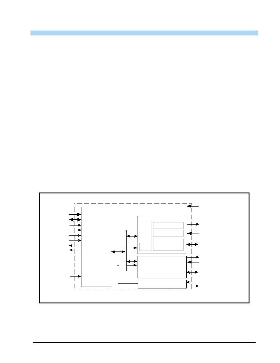
F
IGURE
1. XR16L2450 B
LOCK
D
IAGRAM
XTAL1
XTAL2
Crystal Osc/Buffer
TXA
RTSA#, CTSA#,
DTRA#, DSRA#,
CDA#, RIA#, OP2A#
8-bit Data
Bus
Interface
UART Channel A
BRG
THR
UART
Regs
2.25 to 5.5 Volt VCC
UART Channel B
(same as Channel A)
A2:A0
D7:D0
CSA#
CSB#
INTA
INTB
IOW#
IOR#
Reset
RHR
Modem I/Os
RXA
TXB
RTSB#, CTSB#,
DTRB#, DSRB#,
CDB#, RIB#, OP2B#
RXB
*5V Tolerant inputs
XR16L2450
xr
2.25V TO 5.5V DUART
REV. 1.1.0
2
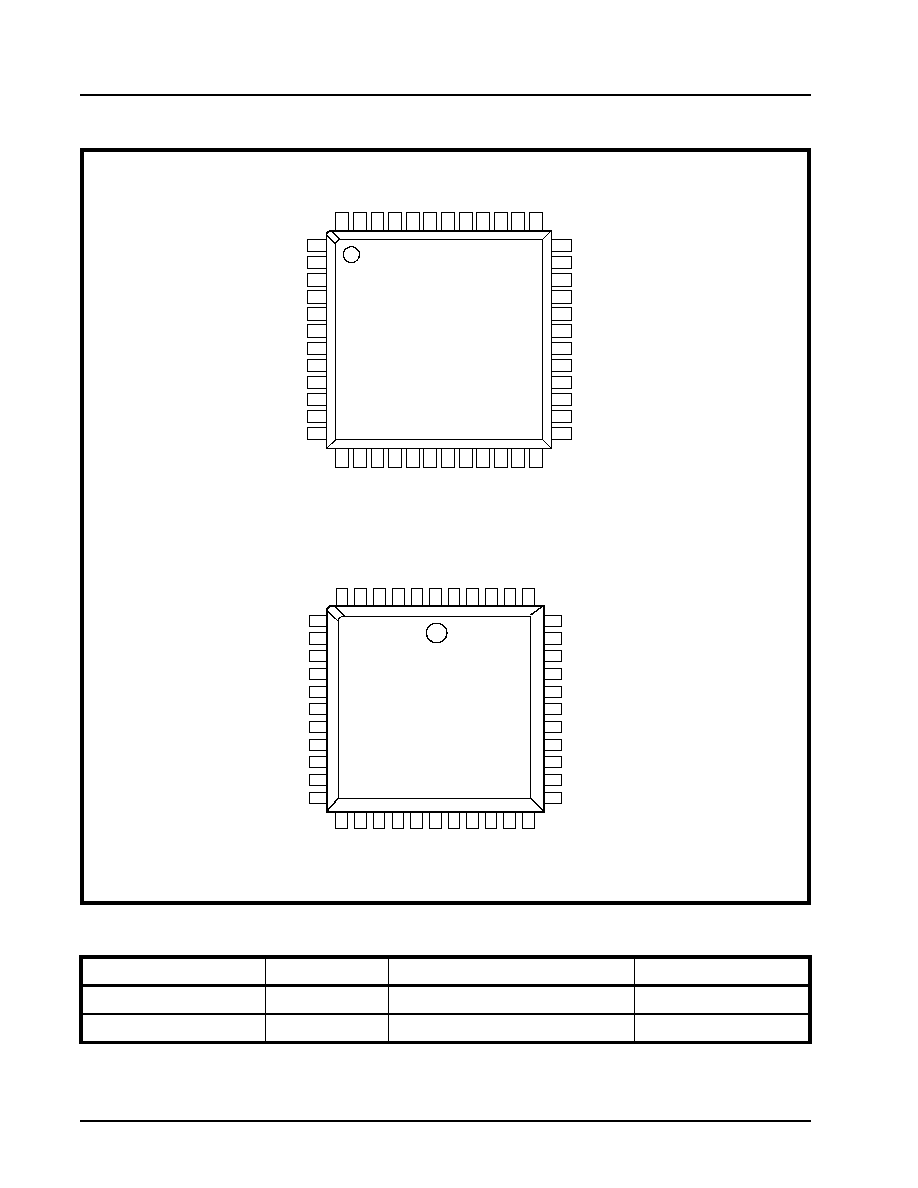
Device
F
IGURE
2. P
IN
O
UT
A
SSIGNMENT
ORDERING INFORMATION
P
ART
N
UMBER
P
ACKAGE
O
PERATING
T
EMPERATURE
R
ANGE
D
EVICE
S
TATUS
XR16L2450IJ
44-Lead PLCC
-40°C to +85°C
Active
XR16L2450IM
48-Lead TQFP
-40°C to +85°C
Active
48
47
46
45
44
43
42
41
40
39
38
37
1
2
3
4
5
6
7
8
9
10
11
12
36
35
34
33
32
31
30
29
28
27
26
25
13
14
15
16
17
18
19
20
21
22
23
24
D5
D6
D7
RXB
RXA
NC
TXA
TXB
OP2B#
CSA#
CSB#
NC
XT
AL1
XT
AL2
IO
W
#
CDB
#
GND
NC
IOR
#
DSRB
#
RI
B
#
RT
SB
#
CT
SB
#
NC
RESET
DTRB#
DTRA#
RTSA#
OP2A#
NC
INTA
INTB
A0
A1
A2
NC
D4
D3
D2
D1
D0
NC
VCC
RI
A#
CDA#
DSRA
#
CT
SA
#
NC
XR16L2450
48-pin TQFP
6
5
4
3
2
1
44
43
42
41
40
7
8
9
10
11
12
13
14
15
16
17
39
38
37
36
35
34
33
32
31
30
29
18
19
20
21
22
23
24
25
26
27
28
D5
D6
D7
RXB
RXA
NC
TXA
TXB
OP2B#
CSA#
CSB#
RESET
DTRB#
DTRA#
RTSA#
OP2A#
NC
INTA
INTB
A0
A1
A2
XT
AL
1
XT
AL
2
IO
W
#
CD
B#
GND
NC
IO
R
#
DS
RB
#
RI
B#
RT
S
B
#
CT
S
B
#
D4
D3
D2
D1
D0
NC
VC
C
RI
A#
CD
A#
DS
RA
#
CT
SA
#
XR16L2450
44-pin PLCC
xr
XR16L2450
REV. 1.1.0
2.25V TO 5.5V DUART
3
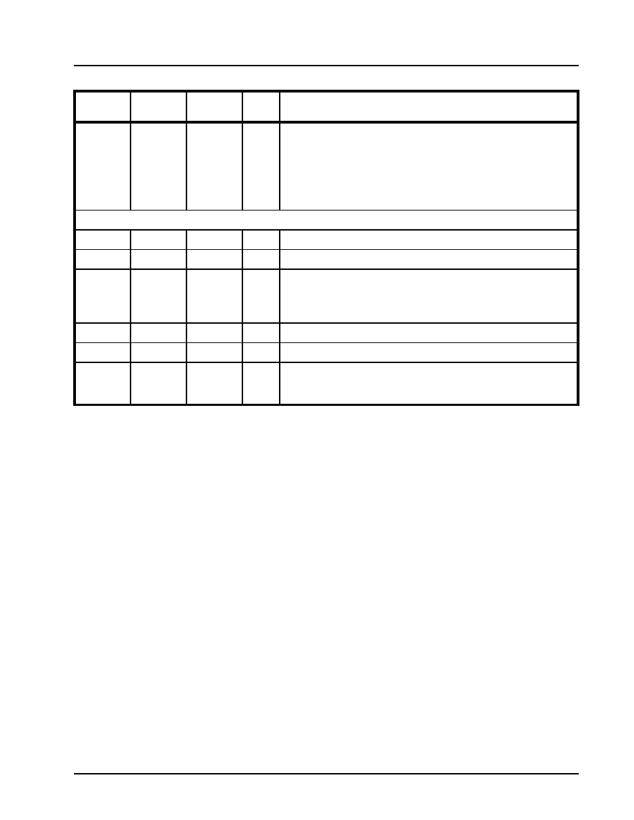
PACKAGE PIN DESCRIPTIONS
PIN DESCRIPTIONS
N
AME
44-PLCC
P
IN
#
48-TQFP
P
IN
#
T
YPE
D
ESCRIPTION
DATA BUS INTERFACE
A2
A1
A0
29
30
31
26
27
28
I
Address data lines [2:0]. These 3 address lines select one of the inter-
nal registers in UART channel A/B during a data bus transaction.
D7
D6
D5
D4
D3
D2
D1
D0
9
8
7
6
5
4
3
2
3
2
1
48
47
46
45
44
IO
Data bus lines [7:0] (bidirectional).
IOR#
24
19
I
Input/Output Read Strobe (active low). The falling edge instigates an
internal read cycle and retrieves the data byte from an internal register
pointed to by the address lines [A2:A0]. The data byte is placed on the
data bus to allow the host processor to read it on the rising edge.
IOW#
20
15
I
Input/Output Write Strobe (active low). The falling edge instigates an
internal write cycle and the rising edge transfers the data byte on the
data bus to an internal register pointed by the address lines.
CSA#
16
10
I
UART channel A select (active low) to enable UART channel A in the
device for data bus operation.
CSB#
17
11
I
UART channel B select (active low) to enable UART channel B in the
device for data bus operation.
INTA
33
30
O
UART channel A Interrupt output. The output state is defined by the
user and through the software setting of MCR[3]. INTA is set to the
active mode and OP2A# output to a logic 0 when MCR[3] is set to a
logic 1. INTA is set to the three state mode and OP2A# to a logic 1
when MCR[3] is set to a logic 0 (default).
INTB
32
29
O
UART channel B Interrupt output. The output state is defined by the
user and through the software setting of MCR[3]. INTB is set to the
active mode and OP2B# output to a logic 0 when MCR[3] is set to a
logic 1. INTB is set to the three state mode and OP2B# to a logic 1
when MCR[3] is set to a logic 0 (default).
MODEM OR SERIAL I/O INTERFACE
TXA
13
7
O
UART channel A Transmit Data. If it is not used, leave it unconnected.
RXA
11
5
I
UART channel A Receive Data. Normal receive data input must idle at
logic 1 condition. If it is not used, tie it to VCC or pull it high via a 100k
ohm resistor.
RTSA#
36
33
O
UART channel A Request-to-Send (active low) or general purpose out-
put. If it is not used, leave it unconnected.
XR16L2450
xr
2.25V TO 5.5V DUART
REV. 1.1.0
4
CTSA#
40
38
I
UART channel A Clear-to-Send (active low) or general purpose input.
This input should be connected to VCC when not used. This input has
no effect on the UART.
DTRA#
37
34
O
UART channel A Data-Terminal-Ready (active low) or general purpose
output. If it is not used, leave it unconnected.
DSRA#
41
39
I
UART channel A Data-Set-Ready (active low) or general purpose input.
This input should be connected to VCC when not used. This input has
no effect on the UART.
CDA#
42
40
I
UART channel A Carrier-Detect (active low) or general purpose input.
This input should be connected to VCC when not used. This input has
no effect on the UART.
RIA#
43
41
I
UART channel A Ring-Indicator (active low) or general purpose input.
This input should be connected to VCC when not used. This input has
no effect on the UART.
OP2A#
35
32
O
Output Port 2 Channel A - The output state is defined by the user and
through the software setting of MCR[3]. INTA is set to the active mode
and OP2A# output to a logic 0 when MCR[3] is set to a logic 1. INTA is
set to the three state mode and OP2A# to a logic 1 when MCR[3] is set
to a logic 0. This output should not be used as a general output else it
will disturb the INTA output functionality. If it is not used at all, leave it
unconnected.
TXB
14
8
O
UART channel B Transmit Data. If it is not used, leave it unconnected.
RXB
10
4
I
UART channel B Receive Data. Normal receive data input must idle at
logic 1 condition. If it is not used, tie it to VCC or pull it high via a 100k
ohm resistor.
RTSB#
27
22
O
UART channel B Request-to-Send (active low) or general purpose out-
put. If it is not used, leave it unconnected.
CTSB#
28
23
I
UART channel B Clear-to-Send (active low) or general purpose input.
This input should be connected to VCC when not used. This input has
no effect on the UART.
DTRB#
38
35
O
UART channel B Data-Terminal-Ready (active low) or general purpose
output. If it is not used, leave it unconnected.
DSRB#
25
20
I
UART channel B Data-Set-Ready (active low) or general purpose input.
This input should be connected to VCC when not used. This input has
no effect on the UART.
CDB#
21
16
I
UART channel B Carrier-Detect (active low) or general purpose input.
This input should be connected to VCC when not used. This input has
no effect on the UART.
RIB#
26
21
I
UART channel B Ring-Indicator (active low) or general purpose input.
This input should be connected to VCC when not used. This input has
no effect on the UART.
PIN DESCRIPTIONS
N
AME
44-PLCC
P
IN
#
48-TQFP
P
IN
#
T
YPE
D
ESCRIPTION
xr
XR16L2450
REV. 1.1.0
2.25V TO 5.5V DUART
5
Pin type: I=Input, O=Output, IO= Input/output, OD=Output Open Drain.
OP2B#
15
9
O
Output Port 2 Channel B - The output state is defined by the user and
through the software setting of MCR[3]. INTB is set to the active mode
and OP2B# output to a logic 0 when MCR[3] is set to a logic 1. INTB is
set to the three state mode and OP2B# to a logic 1 when MCR[3] is set
to a logic 0. This output should not be used as a general output else it
will disturb the INTB output functionality. If it is not used, leave it uncon-
nected.
ANCILLARY SIGNALS
XTAL1
18
13
I
Crystal or external clock input.
XTAL2
19
14
O
Crystal or buffered clock output.
RESET
39
36
I
Reset (active high) - A longer than 40 ns logic 1 pulse on this pin will
reset the internal registers and all outputs. The UART transmitter output
will be held at logic 1, the receiver input will be ignored and outputs are
reset during reset period.
VCC
44
42
Pwr
2.25V to 5.5V power supply. All inputs are 5V tolerant.
GND
22
17
Pwr
Power supply common, ground.
N.C.
1, 12, 23,
34
6, 12, 18,
24, 25, 31,
37, 43
-
No Connection. These pins are not connected internally.
PIN DESCRIPTIONS
N
AME
44-PLCC
P
IN
#
48-TQFP
P
IN
#
T
YPE
D
ESCRIPTION
Document Outline