XR16C864.p65
EXAR Corporation, 48720 Kato Road, Fremont, CA 94538
·
(510) 668-7000
·
FAX (510) 668-7017
XR16C864
Rev. 1.10
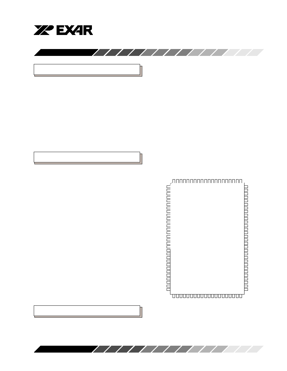
Figure 1, Pinout of the Device
QUAD UART WITH RX/TX FIFO
COUNTERS,128-BYTE FIFO
DESCRIPTION
The XR16C864
1
(864) is a universal asynchronous receiver and transmitter (UART) with a dual interface compatible
with the ST16C554/654/854 and ST68C554. The 864 is an enhanced UART with 128 byte FIFO's, Independent
Transmit and Receive FIFO counters, RS-485 Support, Independent Transmit and Receive DMA signals, automatic
hardware/software flow control, and data rates up to 1.5Mbps. Onboard status registers provide the user with error
indications and operational status, modem interface control. System interrupts may be tailored to meet user
requirements. An internal loop-back capability allows onboard diagnostics. The 864 is available in 100 pin QFP
packages. The XR16C864 offers faster channel status access by providing separate outputs for TXRDY and RXRDY,
offer separate Infrared TX outputs and a separate clock for channel C (CHCCLK) that can be used as a musical
instrument clock input. The 864 combines the package interface modes of the 16C554/654 and 68C554/654 series
on a single integrated chip.
FEATURES
·
Compatibility with the Industry Standard
ST16C554/654, ST68C554/654, TL16C554
·
1.5 Mbps transmit/receive operation (24MHz)
·
128 byte transmit FIFO
·
128 byte receive FIFO with error flags
·
Automatic RS-485 half-duplex switch
·
Independent transmit and receive DMA signals
·
Independent transmit and receive FIFO counter
·
Automatic software/hardware flow control
·
Programmable Xon/Xoff characters
·
Software selectable Baud Rate Generator pre-
scaleable clock rates of 1X, 4X.
·
Four selectable, and Programmable Transmit/
Receive FIFO interrupt trigger levels
·
Standard modem interface or infrared IrDA
encoder/decoder interface
·
Software flow control turned off optionally by any
(Xon) RX character
·
Independent clock input for channel C
·
FIFO monitoring and separate IrDA TX outputs
·
Sleep mode ( 200
µ
A stand-by)
·
100-pin QFP packages
ORDERING INFORMATION
Part number
Pins
Package Operating temperature
XR16C864CQ
100
QFP
0° C to + 70° C
XR16C864IQ
100
QFP
-40° C to + 85° C
Note 1: Covered by US Patent # 5,649,122
July 2000
1
2
3
4
5
6
7
8
9
1 0
1 1
1 2
1 3
1 4
1 5
1 6
1 7
1 8
1 9
2 0
2 1
2 2
2 3
2 4
2 5
2 6
2 7
2 8
2 9
3 0
31
32
33
34
35
36
37
38
39
40
41
42
43
44
45
46
47
48
49
50
10
0
99
98
97
96
95
94
93
92
91
90
89
88
87
86
85
84
83
82
81
8 0
7 9
7 8
7 7
7 6
7 5
7 4
7 3
7 2
7 1
7 0
6 9
6 8
6 7
6 6
6 5
6 4
6 3
6 2
6 1
6 0
5 9
5 8
5 7
5 6
5 5
5 4
5 3
5 2
5 1
B C L K A
-O P 2 A
R S 4 8 5 /-O P 1 A
D A C K A
D R E Q A /-T X R D YA
IR T X A
-D S R A
-C T S A
-D T R A
V C C
-R T S A
IN T A
-C S A
T X A
-IO W
T X B
-C S B
IN T B
-R T S B
G N D
-D T R B
-C T S B
-D S R B
IR T X B
D R E Q B /-T X R D YB
D A C K B
A E N
R S 4 8 5 /-O P 1 B
-O P 2 B
R C L K B
D
R
EQB/-
R
XR
D
Y
B
-CDB
-RI
B
RX
B
C
L
KS
EL
16
/
-
6
8
A2
A1
A0
XT
AL1
XT
AL2
CHCC
L
K
R
ESE
T
-R
X
R
D
Y
-T
X
R
D
Y
GN
D
RX
C
-RI
C
-CDC
D
R
EQC
/
-
R
XR
D
Y
C
B C L K D
-O P 2 D
-O P 1 D /R S 4 8 5
D A C K D
-C S R D Y
IR T X D
-D S R D
-C T S D
-D T R D
G N D
-R T S D
IN T D
-C S D
T X D
-IO R
T X C
-C S C
IN T C
-R T S C
V C C
-D T R C
-C T S C
-D S R C
IR T X C
-T X R D Y C /D R E Q C
D A C K C
T C
-O P 1 C /R S 4 8 5
-O P 2 C
B C L K C
-
R
XR
D
YA/D
R
QA
-CDA
-RI
A
RX
A
GN
D
D7
D6
D5
D4
D3
D2
D1
D0
IN
T
SEL
VC
C
RX
D
-RI
D
-CDD
-
R
X
R
DY
D
/
DR
E
Q
D
-
T
X
R
DY
D
/
DR
E
Q
D
XR16C8
64CQ

XR16C864
2
Rev. 1.10
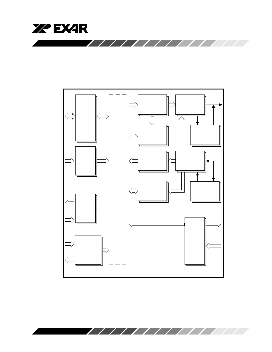
Figure 2, Block Diagram 16 Mode
D0-D7
-IOR
-IOW
RESET
TC
A0-A2
-CS A-D
AEN
INT A-D
-RXRDY A-D
-TXRDY A-D
INTSEL
DREQ A-D
DACK A-D
-DTR A-D
-RTS A-D
-OP1 A-D
RS485 A-D
-CTS A-D
-RI A-D
-CD A-D
-DSR A-D
TX A-D
RX A-D
RXIR A-D
XTAL1
MIDI
XTAL2
BCLK A-D
Da
ta b
u
s
&
C
o
ntr
o
l Lo
gi
c
Re
gi
ster
S
e
l
ect
Lo
gi
c
Modem
Control
Logic
In
te
r
r
u
p
t
Co
n
t
r
o
l
Lo
gi
c
Transmit
FIFO
Registers
Flow
Control
Logic
Transmit
Shift
Register
Receive
FIFO
Registers
Flow
Control
Logic
Receive
Shift
Register
In
te
r
Co
n
n
ec
t
B
u
s Li
n
e
s
&
C
o
ntr
o
l si
gnal
s
Cl
o
c
k
&
Ba
u
d
Ra
te
G
e
n
era
to
r
Ir
Encoder
Ir
Decoder
XR16C864
3
Rev. 1.10
Figure 3, Block Diagram 68 Mode
D 0 -D 7
R /-W
-R E S E T
A 0 -A 4
-C S
A E N
IR Q
-R X R D Y A -D
-T X R D Y A -D
D R E Q A -D
D A C K A -D
-D T R A -D
-R T S A -D
-O P 1 A -D
R S 4 8 5 A -D
-C T S A -D
-R I A -D
-C D A -D
-D S R A -D
T X A -D
R X A -D
R X IR A -D
X T A L 1
C H C C L K
X T A L 2
B C L K A -D
Da
ta
bu
s
&
Co
ntr
ol
L
o
g
i
c
R
egi
st
er
S
elect
Lo
gi
c
M o d e m
C o n tro l
L o g ic
I
nte
r
rup
t
Co
ntr
ol
Lo
gi
c
T r a n s m it
F IF O
R e g iste rs
F lo w
C o n tro l
L o g ic
T r a n s m it
S h ift
R e g iste r
R e c e iv e
F IF O
R e g iste rs
F lo w
C o n tro l
L o g ic
R e c e iv e
S h ift
R e g iste r
I
nte
r
Co
nne
c
t
Bus L
i
n
e
s
&
Co
ntr
ol
s
i
g
nal
s
Cl
oc
k
&
Ba
ud R
a
t
e
Gen
er
at
or
Ir
E n c o d e r
Ir
D e c o d e r
XR16C864
4
Rev. 1.10
SYMBOL DESCRIPTION
Symbol
Pin
Signal
Pin Description
100
type
16/-68
36
I
16/68 Interface Type Select (input with internal pull-up). - This input provides
the 16 (Intel) or 68 (Motorola) bus interface type select. The functions of -IOR,
-IOW, INT A-D, and -CS A-D are re-assigned with the logical state of this pin.
When this pin is a logic 1, the 16 mode interface is selected. When this pin
is a logic 0, the 68 mode interface is selected. When this pin is a logic 0, -
IOW is re-assigned to R/-W, RESET is re-assigned to -RESET, -IOR is not
used, and INT A-D(s) are connected in a WIRE-OR" configuration. The
WIRE-OR outputs are connected internally to the open source IRQ signal
output.
A0
39
I
Address-0 Select Bit. Internal registers address selection in 16 and 68
modes.
A1
38
I
Address-1 Select Bit. Internal registers address selection in 16 and 68
modes.
A2
37
I
Address-2 Select Bit. - Internal registers address selection in 16 and 68
modes.
CLKSEL
35
I
Clock Select. - The pre-scaleable clock is selected by this pin. The div-by-
1 clock is selected when CLKSEL is a logic 1 (connected to VCC) or the div-
by-4 is selected when CLKSEL is a logic 0 (connected to GND). MCR bit-
7 can override the state of this pin following reset or initialization (see MCR
bit-7).
-CSRDY
76
I
Control Status Ready (active low) - The Contents of the FIFORDY Register
is read when this pin is a logic 0. However it should be noted, D0-D3 will
contain the inverted logic states of TXRDY A-D, and D4-D7 the logic states
(un-inverted) of RXRDY A-D.
D0-D2
88-90
I/O
Data Bus (Bi-directional) - These pins are the eight bit, three state data bus
D3-D7
91-95
for transferring information to or from the controlling CPU. D0 is the least
significant bit and the first data bit in a transmit or receive serial data stream.
TC
54
I
Terminal Count. A high pulse terminates a DMA transaction.
AEN
27
I
Address Enable. A high at this input indicates valid DMA cycle. See DACK
pins for DMA cycle description.
sa

XR16C864
5
Rev. 1.10
SYMBOL DESCRIPTION
BCLK A-B
1,30
Baud Rate Generator Output. The baud rate generator clock output is
BCLK C-D
51,80
O
internally connected to the RCLK input. This pin provides the 16X clock of
the selected data rate from the baud rate generator.
OP1 A-B
3,28
OP1, or RS-485 direction control signal. General purpose output during
OP1 C-D
53,78
O
normal operation. RS-485 direction control can be selected when FCTR Bit-
3 is set to "1". During data transmit cycle, OP1/RS-485 pin is low.
DACK A-B
4,26
DMA Acknowledge. DMA cycle will start processing when CPU/Host sets
DACK C-D
55,77
I
this input low and AEN high. All writes will be to the TX FIFO and all reads
will be from the RX FIFO. A0-A2 and -CSA-D will be ignored.
TEST
2,29
52,79
O
Internal circuit test outputs. Not used for normal operation.
GND
96,20
GND
46,71
Pwr
Signal and power ground.
IRTX A-B
6,24
Infrared Transmit Data Output (IrDA) - These pins provide separate infrared
IRTX C-D
57,75
O
IrDA TX outputs for UART channel's (A-D). The serial infrared IRTX data is
transmitted via these pins with added start, stop and parity bits. The IRTX
signal will be a logic 0 during reset, idle (no data), or when the transmitter
is disabled. MCR bit-6 selects the standard modem or infrared interface.
CHCCLK
42
I
Channel C Clock Input - This input provides the clock for UART channel C.
An external 16X baud clock or the crystal oscillator's output, XTAL2, must
be connected to this pin for normal operation. This input may also be used
with MIDI (Music Instrument Digital Interface) applications when an external
MIDI clock is provided.
INTSEL
87
I
Interrupt Select. (active high, with internal pull-down) - This function is
associated with the 16 mode only. When the 16 mode is selected, this pin
can be used in conjunction with MCR bit-3 to enable or disable the three state
interrupts, INT A-D or override MCR bit-3 and force continuous interrupts.
Interrupt outputs are enabled continuously by making this pin a logic 1.
Making this pin a logic 0 allows MCR bit-3 to control the three state interrupt
output: enable outputs when MCR bit-3 is set to a logic "1" and tri-state
outputs when MCR bit-3 is set to a logic "0". This pin should be low for 68
mode.
Symbol
Pin
Signal
Pin Description
100
type