
Parameter
DC Input Voltage Range
DC Output Current Range
Operating Junction Temperature
Ambient Operating Temperature
Symbol
V
IN
I
O
T
jop
T
aop
s
Features
· Compact surface-mount package (SOP-8)
· Output current: 1 A
· Low current consumption: Iq(OFF) ( 1
µ
A (V
C
= 0 V)
· Low dropout voltage: V
DIF
0.8 V (at I
O
= 1 A)
V
DIF
1.2 V (I
O
= 1 A) for SI-3018LSA
· 4 types of output voltages (1.8 V, 2.5 V, 3.3 V, 5.0 V) available
· Output ON/OFF control compatible with LS-TTL
· Built-in foldback overcurrent, thermal protection circuits
s
Applications
· Auxiliary power supply for PC
· Battery-driven electronic equipme
s
Absolute Maximum Ratings
SI-3000LSA Series
Surface-Mount, Low Current Consumption, Low Dropout Voltage Dropper Type
Unit
V
A
W
W
°
C
°
C
°
C
°
C/W
°
C/W
Ratings
16
1
1.16
1.1
30 to +150
30 to +150
30 to +150
36
100
Symbol
V
IN
I
O
P
D1
*1
P
D2
*2
T
j
*3
T
op
T
stg
j-I
j-a
*2
Parameter
DC Input Voltage
DC Output Current
Power Dissipation
Junction Temperature
Ambient Operating Temperature
Storage Temperature
Thermal Resistance (Junction to Lead (pin 8))
Thermal Resistance (Junction to Ambient Air)
(T
a
=25
°
C)
s
Recommended Operating Conditions
*1: V
IN
(max) and I
O
(max) are restricted by the relationship P
D
= (V
IN
V
O
)
×
I
O
.
Calculate these values referring to the reference data.
*2: Refer to the dropout voltage section.
Ratings
SI-3018LSA
SI-3025LSA
SI-3033LSA
SI-3050LSA
3.1 to 3.5
*1
*2
to 3.5
*1
*2
to 5.2
*1
*2
to 8.0
0 to 1
20 to +125
30 to +85
Unit
V
A
°
C
°
C
q
SI-3000LSA Series
*1: When mounted on glass-epoxy board 56.5
×
56.5 mm (copper laminate area 100%)
*2: When mounted on glass-epoxy board 40
×
40 mm (copper laminate area 100%).
*3: Thermal protection circuits may operate if the junction temperature exceeds 135
°
C

*1: Is
1
is specified as the 5% drop point of output voltage V
O
on the condition that V
IN
= 3.3 V (5 V for SI-3033LSA), and I
O
= 0.5 A.
*2: Output is OFF when the output control terminal V
C
is open. Each input level is equivalent to that for LS-TTL. Therefore, it is possible to be
driven directly by an LS-TTL circuit.
The SI-3000LSA series employs a foldback-type overcurrent protection circuit.
*3: In applications in which a certain current is required for start-up, this circuit may cause a start-up error, and therefore the SI-3000LSA series
is not recommended for use in such applications.
(1) Constant current load (2) Dual polarity power supply (3) Series power supply (4) V
O
adjustment by raising ground voltage
s
External Dimensions
(Unit : mm)
s
Electrical Characteristics
(T
a
=25
°
C, V
C
=2V unless otherwise specified)
Unit
V
V
mV
mV
mV/
°
C
dB
mA
µ
A
A
V
µ
A
µ
A
V
Symbol
V
O
Conditions
V
DIF
Conditions
Conditions
V
LINE
Conditions
V
OLOAD
Conditions
V
O
/
T
a
Conditions
R
REJ
Conditions
I
q
Conditions
I
q
(OFF)
Conditions
I
S1
Conditions
V
C
, IH
V
C
, IL
I
C
, IH
Conditions
I
C
, IL
Conditions
V
O
Conditions
0.995max.
0.10
1.27
0.4
±
0.1
0.4
±
0.1
0.15
+0.1
5.1
±
0.4
1.27
8
7
6
5
1
2
3
4
4.4
±
0.2
1.5
±
0.1
1.55
±
0.15
0.05
±
0.05
6.2
±
0.3
0~10
°
0.5
±
0.1
0.05
0.12 M
Pin Arrangement
q
V
IN
w
NC (Leave open)
e
V
IN
r
V
C
t
GND
y
GND
u
V
O
i
V
O
Plastic Mold Package Type
Flammability: UL94V-0
Weight: Approx. 0.1g
q
SI-3000LSA Series
Ratings
SI-3018LSA
SI-3025LSA
SI-3033LSA
SI-3050LSA
min.
typ.
max.
min.
typ.
max.
min.
typ.
max.
min.
typ.
max.
1.764
1.800
1.836
2.450
2.500
2.550
3.234
3.300
3.366
4.90
5.00
5.10
V
IN
=3.3V, I
O
=0.5A
V
IN
=3.3V, I
O
=0.5A
V
IN
=5V, I
O
=0.5A
V
IN
=6.5V, I
O
=0.5A
0.4
0.4
0.4
I
O
0.5A
I
O
0.5A
I
O
0.5A
0.6
1.2
0.8
0.8
0.8
I
O
1A
2
10
2
10
3
10
15
V
IN
=3.1 to 3.5V, I
O
=0.3A
V
IN
=3.1 to 3.5V, I
O
=0.3A
V
IN
=4.5 to 5.5V, I
O
=0.3A
V
IN
=6 to 7V, I
O
=0.3A
10
20
10
20
10
20
30
V
IN
=3.3V, I
O
=0 to 1A
V
IN
=3.3V, I
O
=0 to 1A
V
IN
=5V, I
O
=0 to 1A
V
IN
=6.5V, I
O
=0 to 1A
±
0.3
±
0.3
±
0.3
±
0.5
V
IN
=3.3V, I
O
=5mA, T
j
=0 to 100
°
C
V
IN
=3.3V, I
O
=5mA, T
j
=0 to 100
°
C
V
IN
=5V, I
O
=5mA, T
j
=0 to 100
°
C
V
IN
=6.5V, I
O
=5mA, T
j
=0 to 100
°
C
60
57
55
55
V
IN
=3.3V, f=100 to 120H
Z
V
IN
=3.3V, f=100 to 120H
Z
V
IN
=5V, f=100 to 120H
Z
V
IN
=6.5V, f=100 to 120H
Z
1.7
2.5
1.7
2.5
1.7
2.5
1.7
2.5
V
IN
=3.3V, I
O
=0A
V
IN
=3.3V, I
O
=0A
V
IN
=5V, I
O
=0A
V
IN
=6.5V, I
O
=0A
1
1
1
1
V
IN
=3.3V, I
O
=0A, V
C
=0V
V
IN
=3.3V, I
O
=0A, V
C
=0V
V
IN
=5V, I
O
=0A, V
C
=0V
V
IN
=6.5V, I
O
=0A, V
C
=0V
1.2
1.2
1.2
1.2
V
IN
=3.3V
V
IN
=3.3V
V
IN
=5V
V
IN
=6V
2.0
2.0
2.0
2.0
0.8
0.8
0.8
0.8
40
80
40
80
40
80
40
80
V
C
=2V
0
5
0
5
0
5
0
5
V
C
=0V
0.5
0.5
0.5
0.5
V
IN
=3.3V, I
O
=0A
V
IN
=3.3V, I
O
=0A
V
IN
=5V, I
O
=0A
V
IN
=6.5V, I
O
=0A
Parameter
Output Voltage
Dropout Voltage
Line Regulation
Load Regulation
Temperature Coeffi-
cient of Output Voltage
Ripple Rejection
Quiescent Circuit
Current
OFF Circuit Current
Overcurrent Protection
Starting Current
*1,3
Control Voltage (Output ON)
*2
Control Voltage (Output OFF)
*2
V
C
Control Current (Output ON)
Pin
Control Current (Output OFF)
Output OFF Voltage

s
Block Diagram
s
Standard External Circuit
s
Reference Data
C
O
: Output capacitor (22
µ
F or larger)
C
IN
: Input capacitor (0.1 to 10
µ
F)
This capacitor is required in the case of an inductive
input line or long wiring.
Tantalum capacitors are recommended for C
1
and C
0
,
particularly at low temperatures.
* Leave pin 2 open.
TSD
+
V
IN
NC
V
IN
V
C
V
O
V
O
GND
GND
1
2
3
4
8
7
6
5
1
2
3
4
8
7
6
5
+
V
IN
V
IN
V
C
V
O
C
IN
C
O
GND
+
Load
PWB Copper Laminate Area vs. Junction
to Ambient Air Thermal Resistance
Allowable Output Current
(vs. V
IN
-V
OUT
Voltage Difference)
V
IN
-I
O
max
q
SI-3000LSA Series
150
140
130
120
110
100
90
80
70
100
1000
5000
Copper Laminate Area (mm
2
)
PWB (glass-epoxy, 40
×
40mm)
160mm (40
×
40) mm
j-a
(
°
C/W)
1.2
1.0
0.8
0.6
0.4
0.2
0
1
2
3
4
V
IN
-V
OUT
Voltage Difference (V)
T
j
= 120
°
C (20% derating of 150
°
C)
I
out (
max) (A)
T
a
=25
°
C
T
a
=85
°
C
j-a
=100
°
C/W
The inner frame stage, on which the PTr is mounted, is directly connected to the V
OUT
pin.
Therefore, enlarging the copper laminate area achieves a heat radiation effect of the V
OUT
pin.
s
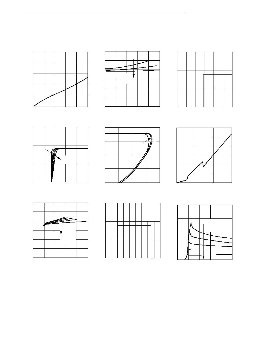
Typical Characteristics of SI-3018LSA
(T
a
=25
°
C)
I
O
vs. V
DIF
Characteristics
Load Regulation
Output ON/OFF Control
Output Voltage Characteristics
Overcurrent Protection Characteristics
Output ON/OFF Control Current
Line Regulation
Thermal Protection Characteristics
Circuit Current
[Note on Thermal Protection]
The thermal protection circuit is in-
tended for protection against heat
during instantaneous short-circuiting.
Its operation is not guaranteed for
continuous heating conditions such
as short-circuiting over extended
periods of time.
0
0.2
0.4
0.6
0.8
1.0
1.0
0.8
0.6
0.4
0.2
0
Output Current I
O
(A)
Dropout Voltage V
DIF
(V)
V
IN
=8V
5V
3.2V
0
0.2
0.4
0.6
0.8
1.0
1.84
1.82
1.80
1.78
1.76
1.74
1.72
Output Current I
O
(A)
Output Voltage V
O
(V)
V
IN
=3.3V
I
O
=5mA
0
1
2
3
3
2
1
0
Output ON/OFF Control Voltage V
C
(V)
Output Voltage V
O
(V)
I
O
=0A-1A
0.25A step
0
1
2
3
4
5
3
2
1
0
Input Voltage V
IN
(V)
Output Voltage V
O
(V)
V
IN
=5V
V
IN
=6V
V
IN
=3.2V
2
1.5
1
0.5
0
0
0.5
1
1.5
2
Output Current I
O
(A)
Output Voltage V
O
(V)
V
IN
=3.3V
I
O
=5mA
0
1
2
3
60
50
40
30
20
10
0
Output Control Voltage V
C
(V)
Terminal Control Current l
C
( A)
µ
0
2
4
6
8
10
1.84
1.82
1.80
1.78
1.76
1.74
1.72
Input Voltage V
IN
(V)
Output Voltage V
O
(V)
I
O
= 1A
0.75A
0.5A
0.25A
0A
I
O
=1A-0A
0.25A step
0
2
4
6
8
10
20
15
10
5
0
Input Voltage V
IN
(V)
Ground Current I
G
(mA)
q
SI-3000LSA Series
V
IN
=3.3V
I
O
=5mA
3
2
1
0
0
60
100
140
180
20
Case Temperature T
C
(
°
C)
Output Voltage V
O
(V)

s
Typical Characteristics of SI-3025LSA
(T
a
=25
°
C)
I
O
vs. V
DIF
Characteristics
Load Regulation
Output ON/OFF Control
Output Voltage Characteristics
Overcurrent Protection Characteristics
Output ON/OFF Control Current
Line Regulation
Thermal Protection Characteristics
Circuit Current
[Note on Thermal Protection]
The thermal protection circuit is in-
tended for protection against heat dur-
ing instantaneous short-circuiting. Its
operation is not guaranteed for con-
tinuous heating conditions such as
short-circuiting over extended periods
of time.
0
0.2
0.4
0.6
0.8
1.0
1.0
0.8
0.6
0.4
0.2
0
Output Current I
O
(A)
Dropout Voltage V
DIF
(V)
V
IN
=10V
8V
5V
3.2V
0
0.2
0.4
0.6
0.8
1.0
2.58
2.56
2.54
2.52
2.50
2.48
2.46
Output Current I
O
(A)
Output Voltage V
O
(V)
V
IN
=3.3V
I
O
=5mA
0
1
2
3
3
2
1
0
Output ON/OFF Control Voltage V
C
(V)
Output Voltage V
O
(V)
I
O
=0A-1A
0.25A step
0
1
2
3
4
5
3
2
1
0
Input Voltage V
IN
(V)
Output Voltage V
O
(V)
V
IN
=3.2V
5V
6V
3
2
1
0
0
0.5
1
1.5
2
Output Current I
O
(A)
Output Voltage V
O
(V)
V
IN
=3.3V
I
O
=5mA
0
1
2
3
60
50
40
30
20
10
0
Output Control Voltage V
C
(V)
Terminal Control Current l
C
( A)
µ
I
O
=1A
0.75A
0.5A
0.25A
0A
0
2
4
6
8
12
10
2.58
2.56
2.54
2.52
2.50
2.48
2.46
Input Voltage V
IN
(V)
Output Voltage V
O
(V)
V
IN
=3.3V
I
O
=5mA
3
2
1
0
0
60
100
140
180
20
Case Temperature T
C
(
°
C)
Output Voltage V
O
(V)
I
O
=1A-0A
0.25A step
0
2
4
6
8
10
20
15
10
5
0
Input Voltage V
IN
(V)
Ground Current I
G
(mA)
q
SI-3000LSA Series