DL5000.fm5
Device
Gates
Logic
Blocks
Input
Blocks
Output
Blocks
Flip Flops
Clock
Trees
DL5064
1,250
64
48
49
212
6
DL5256
5,000
256
76
76
664
6
DL5528
10,000
528
104
112
1,272
6
Features
· Fast Field Programmable Gate Arrays
TM
· Patented Active Repeater
TM
Architecture
· Data and Clock Rates up to 270 MHz
· Complex operations up to 200 MHz
· Input Block Register Setup Time 800 ps
· Output Block Register Clock-to-out 1.6 ns
· ECL, PECL and GTL Interface Levels
· 100K and 100KH Compatible
· Differential Outputs
· 1,000 to 10,000 Gates
· 6 Low-skew Clock Trees
· Highly Predictable, Fanout Independent
Routing Delays
· SRAM-based Programming
· JTAG Boundary Scan
· Fully Automatic Implementation Using
DynaTool
TM
Applications Examples
·
Telecommunications and
Datacommunications
Sonet and ATM Interfaces
Satellite Communications
FDDI
· Test and Instrumentation
VLSI and Memory Testers
Oscilloscopes and Logic Analyzers
· High-Speed Graphics
Real-Time Video Imaging
HDTV
· Servers and Peripherals
High-speed Servers
High-speed Bus Interfaces
Fast Graphics Interfaces
· Emulation
Introduction
The DL5000 is the industry's first Fast Field Pro-
grammable Gate Array (FFPGA
TM
) family. Utilizing
a breakthrough in field programmable interconnect
techniques called
Active Repeaters
, this family pro-
vides unprecedented system level performance.
High operating frequencies combined with fast
ECL, GTL and PECL input and output structures
make these devices ideal for high-speed interfac-
es, subsystems and core logic.
DL5000 family devices are ideal for applications
where other FPGAs can not meet performance re-
quirements. They are also ideal for applications
where designers want to integrate many discrete
ECL devices.
Benefits to the user include ultra high-speed, fast
time-to-market, reduced risk and maximum de-
sign flexibility.
The DL5000 features SRAM-based programming
allowing the devices to be configured in-circuit
and reprogrammed on-the-fly. They can be re-
configured an unlimited number of times provid-
ing maximum flexibility for design iterations and
field upgrades.
DL5256
PG208
9641
DL5000
TM
Family
Fast Field Programmable Gate Array
Datasheet
November 1998

DL5000 - Fast Field Programmable Gate Array
Page 2
November 1998
DynaChip
Table of Contents
Features . . . . . . . . . . . . . . . . . . . . . . . . . . . . . . . . . . . . . . . . . . . . . . . . . . . . . . . . . . . . . . . . . . . . . . . . . . . . . . . . . . . . 1
Applications Examples. . . . . . . . . . . . . . . . . . . . . . . . . . . . . . . . . . . . . . . . . . . . . . . . . . . . . . . . . . . . . . . . . . . . . . . 1
Introduction . . . . . . . . . . . . . . . . . . . . . . . . . . . . . . . . . . . . . . . . . . . . . . . . . . . . . . . . . . . . . . . . . . . . . . . . . . . . . . . . 1
Performance Examples . . . . . . . . . . . . . . . . . . . . . . . . . . . . . . . . . . . . . . . . . . . . . . . . . . . . . . . . . . . . . . . . . . . . . . . 4
High Performance Active Repeater Technology . . . . . . . . . . . . . . . . . . . . . . . . . . . . . . . . . . . . . . . . . . . . . . 4
Active Repeater Architecture . . . . . . . . . . . . . . . . . . . . . . . . . . . . . . . . . . . . . . . . . . . . . . . . . . . . . . . . . . . . . . 6
Input and Output Blocks . . . . . . . . . . . . . . . . . . . . . . . . . . . . . . . . . . . . . . . . . . . . . . . . . . . . . . . . . . . . . . . . . . 8
Logic Block . . . . . . . . . . . . . . . . . . . . . . . . . . . . . . . . . . . . . . . . . . . . . . . . . . . . . . . . . . . . . . . . . . . . . . . . . . . . . . 9
Clock Distribution . . . . . . . . . . . . . . . . . . . . . . . . . . . . . . . . . . . . . . . . . . . . . . . . . . . . . . . . . . . . . . . . . . . . . . . . 9
Detailed Functional Description . . . . . . . . . . . . . . . . . . . . . . . . . . . . . . . . . . . . . . . . . . . . . . . . . . . . . . . . . . . . . 10
Input and Output Blocks . . . . . . . . . . . . . . . . . . . . . . . . . . . . . . . . . . . . . . . . . . . . . . . . . . . . . . . . . . . . . . . . . 10
Logic Blocks . . . . . . . . . . . . . . . . . . . . . . . . . . . . . . . . . . . . . . . . . . . . . . . . . . . . . . . . . . . . . . . . . . . . . . . . . . . . 12
Boundary Scan. . . . . . . . . . . . . . . . . . . . . . . . . . . . . . . . . . . . . . . . . . . . . . . . . . . . . . . . . . . . . . . . . . . . . . . . . . 14
Power Consumption. . . . . . . . . . . . . . . . . . . . . . . . . . . . . . . . . . . . . . . . . . . . . . . . . . . . . . . . . . . . . . . . . . . . . 14
Configuration . . . . . . . . . . . . . . . . . . . . . . . . . . . . . . . . . . . . . . . . . . . . . . . . . . . . . . . . . . . . . . . . . . . . . . . . . . . . . . 14
Configuration Modes . . . . . . . . . . . . . . . . . . . . . . . . . . . . . . . . . . . . . . . . . . . . . . . . . . . . . . . . . . . . . . . . . . . . 14
Mode Pin Settings . . . . . . . . . . . . . . . . . . . . . . . . . . . . . . . . . . . . . . . . . . . . . . . . . . . . . . . . . . . . . . . . . . . . . 14
Serial PROM Configuration Loading Mode . . . . . . . . . . . . . . . . . . . . . . . . . . . . . . . . . . . . . . . . . . . . . . . 15
Microprocessor Interface Loading Mode . . . . . . . . . . . . . . . . . . . . . . . . . . . . . . . . . . . . . . . . . . . . . . . . . 16
Serial Link Loading Mode . . . . . . . . . . . . . . . . . . . . . . . . . . . . . . . . . . . . . . . . . . . . . . . . . . . . . . . . . . . . . . 17
Multi-device Configuration Loading Mode . . . . . . . . . . . . . . . . . . . . . . . . . . . . . . . . . . . . . . . . . . . . . . . 18
Configuration Pins . . . . . . . . . . . . . . . . . . . . . . . . . . . . . . . . . . . . . . . . . . . . . . . . . . . . . . . . . . . . . . . . . . . . . . 19
Permanently Dedicated Pins . . . . . . . . . . . . . . . . . . . . . . . . . . . . . . . . . . . . . . . . . . . . . . . . . . . . . . . . . . . . 19
V
CC
:. . . . . . . . . . . . . . . . . . . . . . . . . . . . . . . . . . . . . . . . . . . . . . . . . . . . . . . . . . . . . . . . . . . . . . . . . . . . . . . 19
V
CCO
: . . . . . . . . . . . . . . . . . . . . . . . . . . . . . . . . . . . . . . . . . . . . . . . . . . . . . . . . . . . . . . . . . . . . . . . . . . . . . 19
V
EE
: . . . . . . . . . . . . . . . . . . . . . . . . . . . . . . . . . . . . . . . . . . . . . . . . . . . . . . . . . . . . . . . . . . . . . . . . . . . . . . . 19
PCLKI: . . . . . . . . . . . . . . . . . . . . . . . . . . . . . . . . . . . . . . . . . . . . . . . . . . . . . . . . . . . . . . . . . . . . . . . . . . . . 19
PCLKO: . . . . . . . . . . . . . . . . . . . . . . . . . . . . . . . . . . . . . . . . . . . . . . . . . . . . . . . . . . . . . . . . . . . . . . . . . . . 19
RESET: . . . . . . . . . . . . . . . . . . . . . . . . . . . . . . . . . . . . . . . . . . . . . . . . . . . . . . . . . . . . . . . . . . . . . . . . . . . . 19
ST PGM: . . . . . . . . . . . . . . . . . . . . . . . . . . . . . . . . . . . . . . . . . . . . . . . . . . . . . . . . . . . . . . . . . . . . . . . . . . . 19
SYS DONE: . . . . . . . . . . . . . . . . . . . . . . . . . . . . . . . . . . . . . . . . . . . . . . . . . . . . . . . . . . . . . . . . . . . . . . . . 19
User Pins That Can Have Special Functions. . . . . . . . . . . . . . . . . . . . . . . . . . . . . . . . . . . . . . . . . . . . . . . 20
DONE: . . . . . . . . . . . . . . . . . . . . . . . . . . . . . . . . . . . . . . . . . . . . . . . . . . . . . . . . . . . . . . . . . . . . . . . . . . . . 20
M0 - M3: . . . . . . . . . . . . . . . . . . . . . . . . . . . . . . . . . . . . . . . . . . . . . . . . . . . . . . . . . . . . . . . . . . . . . . . . . . . 20
SEROUT: . . . . . . . . . . . . . . . . . . . . . . . . . . . . . . . . . . . . . . . . . . . . . . . . . . . . . . . . . . . . . . . . . . . . . . . . . . 20
D0: . . . . . . . . . . . . . . . . . . . . . . . . . . . . . . . . . . . . . . . . . . . . . . . . . . . . . . . . . . . . . . . . . . . . . . . . . . . . . . . . 20
D1 - D7:. . . . . . . . . . . . . . . . . . . . . . . . . . . . . . . . . . . . . . . . . . . . . . . . . . . . . . . . . . . . . . . . . . . . . . . . . . . . 20
WE: . . . . . . . . . . . . . . . . . . . . . . . . . . . . . . . . . . . . . . . . . . . . . . . . . . . . . . . . . . . . . . . . . . . . . . . . . . . . . . . 20
RDY: . . . . . . . . . . . . . . . . . . . . . . . . . . . . . . . . . . . . . . . . . . . . . . . . . . . . . . . . . . . . . . . . . . . . . . . . . . . . . . 20
TDI, TCK, TMS:. . . . . . . . . . . . . . . . . . . . . . . . . . . . . . . . . . . . . . . . . . . . . . . . . . . . . . . . . . . . . . . . . . . . . 20
TDO: . . . . . . . . . . . . . . . . . . . . . . . . . . . . . . . . . . . . . . . . . . . . . . . . . . . . . . . . . . . . . . . . . . . . . . . . . . . . . . 20
GCK1, GCK2: . . . . . . . . . . . . . . . . . . . . . . . . . . . . . . . . . . . . . . . . . . . . . . . . . . . . . . . . . . . . . . . . . . . . . . 20
QCK1, QCK2, QCK3, QCK4:. . . . . . . . . . . . . . . . . . . . . . . . . . . . . . . . . . . . . . . . . . . . . . . . . . . . . . . . . . 21
OLCK, ORCK: . . . . . . . . . . . . . . . . . . . . . . . . . . . . . . . . . . . . . . . . . . . . . . . . . . . . . . . . . . . . . . . . . . . . . . 21
ITCK, IBCK: . . . . . . . . . . . . . . . . . . . . . . . . . . . . . . . . . . . . . . . . . . . . . . . . . . . . . . . . . . . . . . . . . . . . . . . . 21
GSR: . . . . . . . . . . . . . . . . . . . . . . . . . . . . . . . . . . . . . . . . . . . . . . . . . . . . . . . . . . . . . . . . . . . . . . . . . . . . . . 21
RB . . . . . . . . . . . . . . . . . . . . . . . . . . . . . . . . . . . . . . . . . . . . . . . . . . . . . . . . . . . . . . . . . . . . . . . . . . . . . . . . 21
Bpsel: . . . . . . . . . . . . . . . . . . . . . . . . . . . . . . . . . . . . . . . . . . . . . . . . . . . . . . . . . . . . . . . . . . . . . . . . . . . . . 21
Product Specifications . . . . . . . . . . . . . . . . . . . . . . . . . . . . . . . . . . . . . . . . . . . . . . . . . . . . . . . . . . . . . . . . . . . . . . 22
Maximum Ratings. . . . . . . . . . . . . . . . . . . . . . . . . . . . . . . . . . . . . . . . . . . . . . . . . . . . . . . . . . . . . . . . . . . . . . . 22
Operating Conditions . . . . . . . . . . . . . . . . . . . . . . . . . . . . . . . . . . . . . . . . . . . . . . . . . . . . . . . . . . . . . . . . . . . . 22
DC Characteristics Over Operating Conditions . . . . . . . . . . . . . . . . . . . . . . . . . . . . . . . . . . . . . . . . . . . . . . 23
Clock Buffer Switching Characteristics . . . . . . . . . . . . . . . . . . . . . . . . . . . . . . . . . . . . . . . . . . . . . . . . . . . . . 23

DL5000 - Fast Field Programmable Gate Array
DynaChip
November 1998
Page 3
Input and Output Block Switching Characteristics . . . . . . . . . . . . . . . . . . . . . . . . . . . . . . . . . . . . . . . . . . . .24
Logic Block Switching Characteristics. . . . . . . . . . . . . . . . . . . . . . . . . . . . . . . . . . . . . . . . . . . . . . . . . . . . . . .25
Timing Diagrams . . . . . . . . . . . . . . . . . . . . . . . . . . . . . . . . . . . . . . . . . . . . . . . . . . . . . . . . . . . . . . . . . . . . . . . .27
Pin Description . . . . . . . . . . . . . . . . . . . . . . . . . . . . . . . . . . . . . . . . . . . . . . . . . . . . . . . . . . . . . . . . . . . . . . . . . . . . .35
Package Drawings. . . . . . . . . . . . . . . . . . . . . . . . . . . . . . . . . . . . . . . . . . . . . . . . . . . . . . . . . . . . . . . . . . . . . . . . . . .39
204 Super BGA . . . . . . . . . . . . . . . . . . . . . . . . . . . . . . . . . . . . . . . . . . . . . . . . . . . . . . . . . . . . . . . . . . . . . . . . . .39
208 Pin Ceramic PGA . . . . . . . . . . . . . . . . . . . . . . . . . . . . . . . . . . . . . . . . . . . . . . . . . . . . . . . . . . . . . . . . . . . . .40
208 PGA with Heat Sink . . . . . . . . . . . . . . . . . . . . . . . . . . . . . . . . . . . . . . . . . . . . . . . . . . . . . . . . . . . . . . . . . .40
Ordering Information . . . . . . . . . . . . . . . . . . . . . . . . . . . . . . . . . . . . . . . . . . . . . . . . . . . . . . . . . . . . . . . . . . . . . . .41

DL5000 - Fast Field Programmable Gate Array
Page 4
November 1998
DynaChip
Performance Examples
The DL5000 family with DynaChip's patented Active Repeater Architecture sup-
ports data and clock rates up to 270 MHz and performs complex operations up to
200 MHz. The following table shows the performance of functions implemented in
the DL5256 device.
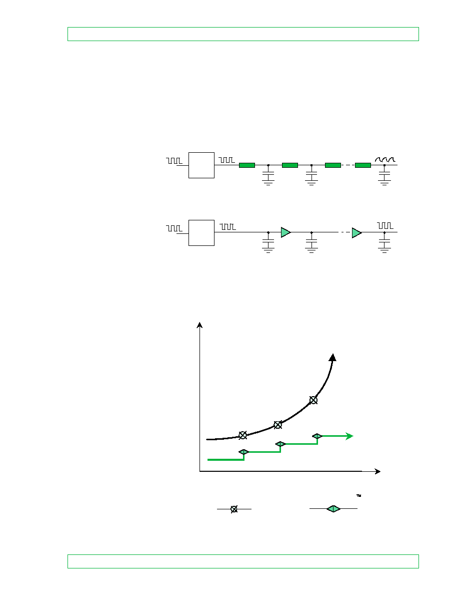
High Performance Active Repeater Technology
The enabling technology behind DynaChip's Fast Field Programmable Gate Arrays
is the Active Repeater.
As shown in figure 1, conventional FPGA devices use pass gates to create program-
mable interconnections. These pass gates act like a series of resistors with distribut-
ed capacitance to ground. Nets formed out of these pass gates slow down
dramatically as the number of programmable connections increases.
This results in long, unpredictable delays, especially for nets that have to travel a
long distance or drive a large number of loads.
Function
DL5256 - G
Logic Block Count
2-bit Shift Register
251 MHz
2
16-bit Synchronous Serial In Shift Register
251 MHz
16
16-bit Loadable Shift Register
Shift
Load
251 MHz
213 MHz
16
16
2 to 1 Mux
Data
Select
251 MHz
213 MHz
1
1
4 to 1 Mux
Data
Select
232 MHz
201 MHz
1
1
Complex Operations to 200 MHz
8-bit Fully Synchronous, Loadable Counter
200 MHz
9
32-bit Fully Synchronous, Loadable Counter
140 MHz
42
64-bit Fully Synchronous, Loadable Counter
120 MHz
86
16 to 1 Mux
Data
Select
116 MHz
100 MHz
5
5
Pipelined Operations
4 x 4 Pipelined Multiplier
170 MHz
49
24-bit Pipelined Adder Accumulator
182 MHz
24
Table 1: Performance of Various Applications
*
*Worst case performance over commercial temperature and voltage range.
DL5000 - Fast Field Programmable Gate Array
DynaChip
November 1998
Page 5
long distance or drive a large number of loads.
In contrast, DynaChip uses Active Repeaters to create programmable interconnec-
tions. These repeaters buffer the signal at every interconnection point and isolate the
capacitance of the rest of the net.
The result is fast, predictable performance even for long, high fanout nets.
Figure 1: Active vs. Passive Interconnect
In FPGA devices that use pass-gate based interconnect, net delays increase quadrat-
ically with the number of programmable interconnect points, as shown in figure 2.
DynaChip devices use Active Repeater interconnect making net delays linear. The
result is much higher performance and greater predictability.
Figure 2: Active Repeater
TM
vs. Passive Interconnect
C
C
R
C
R
R
R
C
C
C
Logic
Block
Logic
Block
Conventional Passive Interconnect
DynaChip's Active Interconnect
Passive Interconnect
Active Repeater
# of Connections
Interconnect Delay