
32 Megabit FLASH EEPROM
DP5Z2ME16Pn3
PRELIMINARY
DESCRIPTION:
The DP5Z2ME16Pn3 `'SLCC'' devices are a revolutionary new memory
subsystem using Dense-Pac Microsystems' ceramic Stackable Leadless Chip
Carriers (SLCC). Available unleaded, straight leaded, `'J'' leaded, gullwing
leaded packages, or mounted on a 50-pin PGA co-fired ceramic substrate.
The Device packs 32-Megabits of FLASH EEPROM in an area as small as 0.463
in
2
, while maintaining a total height as low as 0.131 inches.
The DP5Z2ME16Pn3 is a 2 Meg x 8 FLASH EEPROM memory module. Each
SLCC is hermetically sealed making the module suitable for commercial,
industrial and military applications.
By using SLCCs, the `'Stack'' family of modules offer a higher board density
of memory than available with conventional through-hole, surface mount or
hybrid techniques.
FEATURES:
·
Organization: 2 Meg x 16
·
Fast Access Times: 120, 150, 200ns (max.)
·
Single 5.0 Volt
·
High-Density Symmetrically Blocked Architecture
- Sixteen 128 Kbyte Blocks Per Device
·
Extended Cycling Capability
- 100K Write/Erase Cycles
·
Automated Erase and Program Cycles
- Command User Interface
- Status Register
·
SRAM-Compatible Write Interface
·
Hardware Data Protection Feature
- Erase / Write Lockout during
Power Transitions
·
Packages Available:
DP5Z2ME16PY
48 - Pin SLCC
DP5Z2ME16PI3
48 - Pin Straight Leaded SLCC
DP5Z2ME16PH3
48 - Pin Gullwing Leaded SLCC
DP5Z2ME16PJ3
48 - Pin `'J'' Leaded SLCC
DP5Z2ME16PA3
50 - Pin PGA Dense-SLCC
DP5Z2ME16PJ3
DP5Z2ME16PI3
DP5Z2ME16PY
DP5Z2ME16PH3
DP5Z2ME16PA3
2Mx16, 120 - 200ns, STACK/PGA
30A161-02
A
This document contains information on a product under consideration for
development at Dense-Pac Microsystems, Inc. Dense-Pac reserves the right
to
c
hange or discontinue information on this product without prior notice.
30A161-42
REV. B
1

DP5Z2ME16Pn3
Dense-Pac Microsystems, Inc.
PRELIMINARY
PIN-OUT DIAGRAM
48 - PIN LEADLESS SLCC
48 - PIN STRAIGHT LEADED SLCC
48 - PIN `'J'' LEADED SLCC
48 - PIN GULLWING LEADED SLCC
50 - PIN PGA
DENSE-STACK
FUNCTIONAL BLOCK DIAGRAM
30A161-42
REV. B
2

Dense-Pac Microsystems, Inc.
DP5Z2ME16Pn3
PRELIMINARY
BUS OPERATION
11
Flash memory reads, erases and writes in-system via the local CPU. All bus cycles to or from the flash memory conform to standard
microprocessor bus cycles.
Table 1: Bus Operation
Mode
CE
OE
WE
A0
A1
A9
I/O0-I/O7,
I/O8-I/O15
UB/LB
Read
1, 4
V
IL
V
IL
V
IH
X
X
X
D
OUT
V
IL
/V
IH
Output Disable
1
V
IL
V
IH
V
IH
X
X
X
HIGH-Z
X
Standby
1
V
IH
X
X
X
X
X
HIGH-Z
X
Deep Power-Down
1
X
X
X
X
X
X
HIGH-Z
X
Manufacturer Identifier
1, 3
V
IL
V
IL
V
IH
V
IL
V
IL
V
ID
C2H
V
IL
Device Identifier
3
V
IL
V
IL
V
IH
V
IH
V
IL
V
ID
F1H
V
IL
Write
1, 2
V
IL
V
IH
V
IL
X
X
X
D
IN
V
IL
/V
IH
NOTES:
1. X can be V
IL
or V
IH
for address or control pins.
2. Command for deferent Erase operations, Data program operations or Selector Protect operations can only be successfully completed through proper
command sequence.
3. V
ID
= 11.5V - 12.5V.
4. UB/LB = V
IL
, I/O0-I/O7(I/O8-I/O15) = Lower Bank Data In/Out. UB/LB = V
IH
, I/O0-I/O7(I/O8-I/O15) = Upper Bank Data In/Out.
WRITE OPERATION
Commands are written to the COMMAND INTERFACE REGISTER
(CIR) using standard microprocessor write timing. The CIR serves
as the interface between the microprocessor and the internal chip
operation. The CIR can decipher Read Array, Read Silicon ID,
Erase and Program command. In the event of a read command,
the CIR simply points the read path at either the array or the Silicon
ID, depending on the specific read command given. for a program
or erase cycle, the CIR informs the write state machine that a
program or erase has been requested. During a program cycle,
the write state machine control the program sequences and the
CIR will only respond to status reads. During a sector/chip erase
cycle, the CIR will respond to status reads and erase suspend. After
the writhe state machine has completed its task, it will allow the
CIR to respond to its full command set. The CIR stays at read status
register mode until the microprocessor issues another valid
command sequence.
Device operations are selected by writing commands into the CIR.
Table 3 below defines 16 Megabit Flash family command.
PIN NAMES
A0 - A19
ADDRESS INPUTS: for memory address. Addresses are internally latched during a write cycle.
I/O0 - I/O7,
I/O8 - I/O15
DATA INPUT/OUTPUT: Input data and command during Command Data Interface Register (CIR) write
cycles. Outputs array, status and identifier data in the appropriate read mode. Floated when the chip is
de-selected or the outputs are disabled.
UB/LB
UPPER BANK/LOWER BANK: Used to select upper/lower 1 megabyte memory array banks during reads or
the upper/lower 64 byte banks during 128 byte page writes. This control pin should be used as the LSB
address during reads, but not used in page sector addressing during programming.
CE
CHIP ENABLE INPUT: Activate the device's control logic, Input buffers, decoders and sense amplifiers. With
CE high, the device is de-selected and power consumption reduces to Standby level upon completion of any
current program or erase operation. CE must be low to select the device. Device selection occurs with the
falling edge of CE. The rising edge of CE disables the device.
WE0, WE1
WRITE ENABLES: Controls writes to the Command Interface Register (CIR). WE is active low.
OE
OUTPUT ENABLE: Gates the device's data through the output buffers during a read cycle. OE is active low.
V
DD
DEVICE POWER SUPPLY (+5.0 Volts
±
10%)
V
SS
GROUND
N.C.
No Connect
30A161-42
REV. B
3
DP5Z2ME16Pn3
Dense-Pac Microsystems, Inc.
PRELIMINARY
DEVICE OPERATION
SILICON ID READ
The Silicon ID Read mode allows the reading out of a binary code
from the device and will identify its manufacturer and type. this is
intended for use by programming equipment for the purpose of
automatically matching the device to be programmed with its
corresponding programming algorithm. This mode is functional
over the entire temperature range of the device.
To activate the mode, the programming equipment must force V
ID
(11.5V ~ 12.5V) on address pin A9. Two identifier bytes may then
be sequenced from the device outputs by toggling address A0 from
V
IL
to V
IH
. All addresses are don't cares except A0 and A1.
The manufacturer and device codes may also be read via the
command register, for instance when the device is erased or
programmed in a system without access to high voltage on the A9
pin. The command sequence is illustrated in Table 2.
To terminate the operation, it is necessary to write the read/reset
command sequence into the CIR.
READ RESET COMMAND
The read or reset operation is initiated by writing the read/reset
command sequence into the command register. Microprocessor
read cycles retrieve array data from the memory. The device
remains enabled fro reads until the CIR contents are altered by a
valid command sequence.
The device will automatically power-up in the read/reset state. In
this case, a command sequence is not required to read data. This
default value ensures that no spurious alteration of the memory
content occurs during the power transition. Refer to the AC Read
Characteristics and Waveforms for the specific timing parameters.
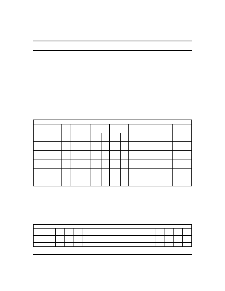
Table 2: Command Definition
Command
Sequence
Bus
Cycles
Req'd
First Bus
Write Cycle
Second Bus
Write Cycle
Third Bus
Write Cycle
Fourth Bus
Read/Write
Cycle
Fifth Bus
Write Cycle
Sixth Bus
Write Cycle
Address Data Address Data Address Data
Address
Data
Address Data Address Data
Read/Reset
4
5555H AAH 2AAAH 55H 5555H F0H
RA
RD
-
-
-
-
Silicon ID Read
4
5555H AAH 2AAAH 55H 5555H 90H 00H/01H C2H/F1H
-
-
-
-
Page/Byte Program
4
5555H AAH 2AAAH 55H 5555H A0H
PA
PD
-
-
-
-
Chip Erase
6
5555H AAH 2AAAH 55H 5555H 80H
5555H
AAH
2AAAH 55H 5555H 10H
Sector Erase
6
5555H AAH 2AAAH 55H 5555H 80H
5555H
AAH
2AAAH 55H
SA
30H
Erase Suspend
3
5555H AAH 2AAAH 55H 5555H B0H
-
-
-
-
-
-
Erase Resume
3
5555H AAH 2AAAH 55H 5555H D0H
-
-
-
-
-
-
Read Status Register
4
5555H AAH 2AAAH 55H 5555H 70H
X
SRD
-
-
-
-
Clear Status Register
3
5555H AAH 2AAAH 55H 5555H 50H
-
-
-
-
-
-
Sleep
3
5555H AAH 2AAAH 55H 5555H C0H
-
-
-
-
-
-
Abort
3
5555H AAH 2AAAH 55H 5555H E0H
-
-
-
-
-
-
NOTES:
1. Address bit A15 - A19, UL/UB = X = Don't Care for all address commands except for Programming Address (PA) and Sector Address (SA).
5555H and 2AAAH address command codes stand for Hex number starting from A0 to A14.
2. Bus operations are defined in Table 2.
3. RA = Address of the memory location to be read.
PA = Address of the memory to be programmed. Addresses are latched on the falling edge of the WE pulse.
SA = Address of the sector to be erased. The combination of A16 - A19 will be uniquely select any sector.
4. RD = Data read from location RA during read operation.
PD = Data to be programmed at location PA. Data is latched on the rising edge of WE.
SRD = Data read from Status Register.
Table 3: Silicon ID Code
Type
A19
A18
A17
A16
A1
A0
Code
(HEX)
I/O7,
I/O15
I/O6,
I/O14
I/O5,
I/O13
I/O4,
I/O12
I/O3,
I/O11
I/O2,
I/O10
I/O1,
I/O9
I/O0,
I/O8
Manufacturer's
Code
X
X
X
X
V
IL
V
IL
C2H
1
1
0
0
0
0
1
0
Device Code
X
X
X
X
V
IL
V
IH
FIH
1
1
1
1
0
0
0
1
30A161-42
REV. B
4

Dense-Pac Microsystems, Inc.
DP5Z2ME16Pn3
PRELIMINARY
PAGE PROGRAM
To initiate Page Program mode, a three-cycle command sequence
is required. There are two "unlock" write cycles. These are
followed by writing the page program command - A0H.
After three-cycle command sequence is given, a byte load is
performed by applying a low pulse on the WE or CE input with CE
or WE low (respectively) and OE high. The address is latched on
the falling edge of CE or WE, whichever occurs last. The data is
latched by the first rising edge of CE or WE. Maximum of 128 bytes
of data may be loaded into each page by the same procedures as
outlined in the page program section below.
BYTE LOAD
Byte loads are used to enter the 128 bytes of a page to be
programmed. A byte load is performed by applying a low pulse
on the WE or CE input CE or WE low respectively) and OE high.
The address is latched on the falling edge of CE or WE, whichever
occurs last. The data is latched by the first rising edge of CE or WE.
The UB/LB control pin is used to select the upper 64 byte bank or
the lower 64 byte bank for each 128 byte page to write the entire
128 byte page, the UB/LB control pin must be used as the LSB
address pin to select both halves of the internal memory array.
PROGRAM
Any page to be programmed should have the page in the erase
state first, i.e. performing sector erase is suggested before page
programming can be performed.
The device is programmed on a page basis. If a byte of data within
a page is to be changed, data for the entire page can be loaded
into the device. Any byte that is not loaded during the
programming of its page will be still in the erase state (i.e. FFH).
Once the bytes of a page are loaded into the device, they are
simultaneously programmed during the internal programming
period. After the first data byte has been loaded into the device,
successive bytes are entered in the same manner. Each new byte
to be programmed must have its high to low transition on WE (or
CE) within 30
µ
s of the low to high transition of WE (or CE) of the
preceding byte. A6 to A19 specify the page address, i.e. the device
is page-aligned on 128 bytes boundary The page address must be
valid during each high to low transition of WE or CE. UB/LB and
A0 to A5 specify the byte address within the page. The byte (word)
may be loaded in any order; sequential loading is not required. If
a high to low transition of CE or WE is not detected within 100
µ
s
of the last low to high transition, the load period will end and the
internal programming period will start. The auto page program
terminates when status on I/O7(I/O15) is "1" at which time the
device stays at read status register mode until the CIR contents are
altered by a valid command sequence. (Refer to Table 2 & 5 and
Figure 1, 6 & 7)
CHIP ERASE
Chip erase is a six-bus cycle operation. There are two "unlock"
write cycles. These are followed by writing the "set-up" command
- 80H. Two more "unlock" write cycles are then followed by the
chip erase command - 10H.
Chip erase does not require the user to program the device prior
to erase.
The automatic erase begins on the rising edge of the last WE pulse
in the command sequence and terminates when the status on
I/O7(I/O15) is "1" at which time the device stays at read status
register mode until the CIR contents are altered by a valid
command sequence. (Refer to Tables 2 & 5 and Figures 2, 6 & 8)
Table 4: Sector Address *
(using UB/LB as LSB)
A19
A18
A17
A16
Address Range
[A0-A15, UB/LB ]
SA0
0
0
0
0
000000H--01FFFFH
SA1
0
0
0
1
020000H--03FFFFH
SA2
0
0
1
0
040000H--05FFFFH
SA3
0
0
1
1
060000H--07FFFFH
SA4
0
1
0
0
080000H--09FFFFH
...
....
...
...
................
SA15
1
1
1
1
1E0000H--1FFFFFH
* Per 2 Meg x 8 device.
SECTOR ERASE
Sector erase is a six-bus cycle operation. There are two "unlock"
write cycles. These are followed by writing the set-up command
- 80H. Two more "unlock" write cycles are then followed by the
sector erase command - 30H. The sector address is latched on the
falling edge of WE, while the command (data) is latched on the
rising edge of WE.
Sector erase does not require the user to program the device prior
to erase. The system is not required to provide any controls or
timings during these operations.
The automatic sector erase begins on the rising edge of the last WE
pulse in the command sequence and terminates when the status
on I/O7(I/O15) is "1" at which time the device stays at read status
register mode. The device remains enabled for read status register
mode until the CIR contents are altered by a valid command
sequence. (Refer to Tables 2, & 5 and Figures 3, 4, 6 & 8)
ERASE SUSPEND
This command only has meaning while the WSM is executing
SECTOR or CHIP erase operations, and therefore will only be
responded to during SECTOR or CHIP erase operation. After this
command has been executed, the CIR will initiate the WSM to
suspend erase operations, and then return to Read Status Register
mode. The WSM will set the I/O6(I/O14) bit to a "1". Once the
WSM has reached the Suspend state, the WSM will set I/O7(I/O15)
bit to a "1". At this time, WSM allows CIR to respond to the Read
Array, Read Status Register, Abort and Erase Resume commands
only. In this mode, the CIR will not respond to any other
commands. the WSM will continue to run, idling in the SUSPEND
state, regardless of the state of all input control pins.
ERASE RESUME
This command will cause the CIR to clear the suspend state and
set the I/O6(I/O14) to a "0", but only in an Erase Suspend command
was previously used. Erase Resume will not have any effect in all
other conditions.
READ STATUS REGISTER COMMAND
The module contains a Status Register which may be read to
determine when a program or erase operation is complete, and
whether that operation completed successfully. The status register
may be read at any time by writing the Read Status command to
the CIR. After writing this command, all subsequent read
operations output data from the status register, until another valid
command is written to the CIR. A Read Array command must be
written to the CIR to return to the Read Array mode.
30A161-42
REV. B
5