
1 of 157
093002
Note: Some revisions of this device may incorporate deviations from published specifications known as errata. Multiple revisions of any device
may be simultaneously available through various sales channels. For information about device errata, click here:
www.maxim-ic.com/errata
.
GENERAL DESCRIPTION
The DS2196 T1 dual framer LIU is designed for T1
transmission equipment. The DS2196 combines dual
optimized framers together with a LIU. This
combination allows the users to extract and insert
facility data-link (FDL) messages in the receive and
transmit paths, collect line performance data, and
perform basic channel conditioning and maintenance.
The DS2196 contains all of the necessary functions
for connection to T1 lines whether they are DS1 long
haul or DSX�1 short haul. The clock recovery
circuitry automatically adjusts to T1 lines from 0ft to
over 6000ft in length. The device can generate both
DSX�1 line buildouts as well as CSU line buildouts
of -7.5dB, -15dB, and -22.5dB. The on-board jitter
attenuator (selectable to either 32 bits or 128 bits) can
be placed in either the transmit or receive data paths.
The framer locates the frame and multiframe
boundaries and monitors the data stream for alarms.
The device contains a set of internal registers that the
user can access and use to control the unit's operation
of the unit. Quick access through the parallel control
port allows a single controller to handle many T1
lines. The device fully meets all of the latest T1
specifications.
PACKAGE OUTLINE
FEATURES
�
Two full-featured framers and a short/long-haul
line interface unit (LIU) in one small package
�
Based on Dallas Semiconductor's single -chip
transceiver (SCT) family
�
Two HDLC controllers with 64-byte buffers that
can be used for the FDL or DS0 channels
�
Supports NPRMs and SPRMs as per ANSI
T1.403-1998
�
Can be combined with a short/long-haul LIU or a
HDSL modem chipset to create a low-cost office
repeater/NIU/CSU, or a HDSL1/HDSL2 terminal
unit with enhanced monitoring and data link
control
�
Supports fractional T1
�
Can convert from D4 to ESF framing and ESF to
D4 framing
�
32-bit or 128-bit crystal-less jitter attenuator
�
Can generate and detect repeating in-band
patterns from 1 to 8 bits or 16 bits in length
�
Detects and generates RAI-CI and AIS-CI
�
Generates DS1 idle codes
�
On-chip programmable BERT generator and
detector
�
All key signals are routed to pins to support
numerous hardware configurations
�
Supports both NRZ and bipolar interfaces
�
Can create errors in the F-bit position and BERT
interface data paths
�
8-bit parallel control port that can be used
directly on either multiplexed or nonmultiplexed
buses (Intel or Motorola)
�
IEEE 1149.1 JTAG Boundary Scan
�
3.3V supply with 5V tolerant inputs and outputs
�
100-pin LQFP (14 mm x 14 mm) package
ORDERING INFORMATION
PART
TEMP RANGE
PIN-PACKAGE
DS2196L
0�C to +70�C
100 LQFP
DS2196LN
-40�C to +85�C
100 LQFP
www.maxim-ic.com
DS2196
T1 Dual Framer LIU
1
100
DS2196

DS2196
2 of 157
TABLE OF CONTENTS
1
INTRODUCTION................................................................................................................................ 6
1.1 FEATURE HIGHLIGHTS.................................................................................................................. 6
1.2 TYPICAL APPLICATIONS............................................................................................................. 10
1.3 FUNCTIONAL DESCRIPTION....................................................................................................... 10
2
PIN DESCRIPTION .......................................................................................................................... 10
3
PIN FUNCTION DESCRIPTION.................................................................................................... 13
4
REGISTER MAP............................................................................................................................... 21
5
PARALLEL PORT............................................................................................................................ 27
6
CONTROL, ID, AND TEST REGISTERS ..................................................................................... 27
7 STATUS AND INFORMATION REGISTERS ............................................................................ 51
8 ERROR COUNT REGISTERS....................................................................................................... 64
9
SIGNALING OPERATION.............................................................................................................. 68
10 DS0 MONITORING FUNCTION .................................................................................................. 70
11 PER�CHANNEL CODE (IDLE) GENERATION AND LOOPBACK ..................................... 72
11.1 TRANSMIT SIDE CODE GENERATION .................................................................................. 72
11.2 RECEIVE SIDE CODE GENERATION...................................................................................... 73
12 PROGRAMMABLE IN�BAND CODE GENERATION AND DETECTION ......................... 74
13 CLOCK BLOCKING REGISTERS.............................................................................................. 83
14 TRANSMIT TRANSPARENCY.................................................................................................... 85
15 BERT FUNCTION .......................................................................................................................... 86
15.1 BERT REGISTER DESCRIPTION.............................................................................................. 88
16 ERROR INSERTION FUNCTION ............................................................................................... 96
17 HDLC CONTROLLER .................................................................................................................. 99
17.1 HDLC
FOR
DS0
S
......................................................................................................................... 100
18 FDL/FS EXTRACTION AND INSERTION .............................................................................. 101
18.1 HDLC AND BOC CONTROLLER FOR THE FDL.................................................................. 101
18.1.1 General Overview................................................................................................................. 101
18.1.2 Status Register for the HDLC............................................................................................... 103
18.1.3 Basic Operation Details ........................................................................................................ 103
18.1.4 HDLC/BOC Register Description ........................................................................................ 105

DS2196
3 of 157
18.2 LEGACY FDL SUPPORT.......................................................................................................... 115
18.2.1 Overview............................................................................................................................... 115
18.2.2 Receive Section..................................................................................................................... 115
18.2.3 Transmit Section................................................................................................................... 116
18.3 D4/SLC�96 OPERATION .......................................................................................................... 117
19
LINE INTERFACE FUNCTION................................................................................................ 118
19.1 RECEIVE CLOCK AND DATA RECOVERY ......................................................................... 118
19.2 TRANSMIT WAVESHAPING AND LINE DRIVING............................................................. 119
19.3 JITTER ATTENUATOR .......................................................................................................... 120
20
JTAG-BOUNDARY SCAN ARCHITECTURE AND TEST ACCESS PORT...................... 124
20.1 D
ESCRIPTION
................................................................................................................................ 124
20.2 TAP C
ONTROLLER
S
TATE
M
ACHINE
............................................................................................ 125
20.3 I
NSTRUCTION
R
EGISTER AND
I
NSTRUCTIONS
................................................................................ 127
21
TIMING DIAGRAMS.................................................................................................................. 133
22
OPERATING PARAMETERS ................................................................................................... 141
23
100-PIN LQFP PACKAGE SPECIFICATIONS ...................................................................... 157

DS2196
4 of 157
LIST OF FIGURES
Figure 1-1: T1 Dual Framer LIU .............................................................................................................. 9
Figure 15-1: BERT Mux Diagram .......................................................................................................... 87
Figure 19-1: External Analog Connections .......................................................................................... 121
Figure 19-2: Jitter Tolerance ................................................................................................................. 122
Figure 19-3: Transmit Waveform Template........................................................................................ 122
Figure 19-4: Jitter Attenuation.............................................................................................................. 123
Figure 20-1: Boundary Scan Architecture ........................................................................................... 124
Figure 20-2: TAP Controller State Machine........................................................................................ 127
Figure 21-1: Receive Side D4 Timing.................................................................................................... 133
Figure 21-2: Receive Side ESF Timing ................................................................................................. 134
Figure 21-3: Receive Side Boundary Timing ....................................................................................... 135
Figure 21-4: Transmit Side D4 Timing................................................................................................. 136
Figure 21-5: Transmit Side ESF Timing .............................................................................................. 137
Figure 21-6: Transmit Side Boundary Timing .................................................................................... 138
Figure 21-7: Transmit Data Flow.......................................................................................................... 139
Figure 21-8: Receive Data Flow............................................................................................................. 140
Figure 22-1: Intel Bus Read AC Timing (BTS=0 / MUX = 1) ............................................................ 146
Figure 22-2: Intel Bus Write Timing (BTS=0 / MUX=1) .................................................................... 147
Figure 22-3: Motorola Bus AC Timing (BTS = 1 / MUX = 1) ............................................................ 148
Figure 22-4: Intel Bus Read AC Timing (BTS=0 / MUX=0) .............................................................. 149
Figure 22-5: Intel Bus Write AC Timing (BTS=0 / MUX=0) ............................................................. 150
Figure 22-6: Motorola Bus Read AC Timing (BTS=1 / MUX=0) ...................................................... 151
Figure 22-7: Motorola Bus Write AC Timing (BTS=1 / MUX=0) ..................................................... 152
Figure 22-8: Receive Side AC Timing................................................................................................... 153
Figure 22-9: Receive Line Interface AC Timing.................................................................................. 154
Figure 22-10: Transmit Side AC Timing.............................................................................................. 155
Figure 22-11: Transmit Line Interface Side AC Timing..................................................................... 156

DS2196
5 of 157
LIST OF TABLES
Table 2-1: Pin Description Sorted by Pin Number................................................................................ 10
Table 4-1: Register Map Sorted by Address .......................................................................................... 21
Table 6-1: Output Pin Test Modes .......................................................................................................... 36
Table 6-2: Receive Data Source Mux Modes......................................................................................... 37
Table 6-3: TPOSB/TNEGB Data Source Select..................................................................................... 38
Table 7-1: Receive T1 Level Indication .................................................................................................. 57
Table 7-2: Alarm Criteria ........................................................................................................................ 59
Table 8-1: Line Code Violation Counting Arrangements..................................................................... 66
Table 8-2: Path Code Violation Counting Arrangements..................................................................... 67
Table 8-3: Multiframes Out Of Sync Counting Arrangements............................................................ 67
Table 12-1: Transmit Code Length......................................................................................................... 75
Table 12-2: Receive Code Length ........................................................................................................... 75
Table 15-1: Bert Pattern Select Options................................................................................................. 89
Table 15-2: Repetitive Pattern Length Options..................................................................................... 90
Table 15-3: Bert Rate Insertion Select.................................................................................................... 91
Table 16-1: Error Rate Options .............................................................................................................. 98
Table 16-2: Error Insertion examples..................................................................................................... 99
Table 17-1: Transmit HDLC Configuration .......................................................................................... 99
Table 18-1: HDLC/BOC Controller Register List............................................................................... 102
Table 19-1: Line Build Out Select In LICR ......................................................................................... 119
Table 19-2: Transformer Specifications ............................................................................................... 120
Table 20-1: Instruction Codes For The DS21352/552 IEEE 1149.1 Architecture............................ 128
Table 20-2: ID Code Structure .............................................................................................................. 128
Table 20-3: Device ID Codes.................................................................................................................. 129
Table 20-4: Boundary Scan Register Description................................................................................ 130

DS2196
6 of 157
1. INTRODUCTION
The DS2196 is a derivative of the DS21352 T1 SCT. The feature set has been optimized for transport
applications commonly found in T1 transmission equipment. The DS2196 register map and register bit
definitions are compatible with the DS21352/DS21552, allowing for easy migration to the DS2196.
Interface designs requiring per-channel code insertion, elastic stores, and ANSI 1's density monitoring
should use the DS21352 or DS21552.
1.1 Feature Highlights
� Main features
� Two full-featured independent framers
� Short/long haul LIU
� 100-pin LQFP small package
� 3.3V operation with 5V tolerant I/O
� 8-bit parallel control port
� Multiplexed or nonmultiplexed buses
� Intel or Motorola formats
� Polled or interrupt environments
� HDLC Support
� Two independent HDLC controllers
� 64-byte Rx and Tx buffers
� Access FDL or single/multiple DS0
channels
� ANSI T1.403-1998 support
� NPRMs
� SPRMs
� RAI-CI detection and generation
� AIS-CI detection and generation
� Format Conversion
� D4 to ESF framing
� ESF to D4 framing
� LIU
� Long and short-haul support
� Receive sensitivity: 0dB to -36dB
� 32-bit or 128-bit crystal-less jitter
attenuator
� DSX-1 and CSU line buildout options
� Provisions for custom waveform
generation
� DS1 Idle Code Generation
� User-defined
� Fixed 7F Hex
� Digital milliwatt
� In-band repeating pattern generator and
detector
� Programmable pattern generator
� Three programmable pattern detectors
� Patterns from 1 to 8 bits or 16 bits in
length
� Programmable on-chip bit error-rate testing
� Pseudorandom patterns including QRSS
� User-defined repetitive patterns
� Daly pattern
� Error insertion
� Bit and error counts
� Payload Error Insertion
� Error insertion in the payload portion of
the T1 frame in the transmit path
� Errors can be inserted over the entire
frame or selected channels
� Insertion options include continuous and
absolute number with selectable insertion
rates
� Function Isolation
� All key signals are routed to pins
� LIU, Framer A, and Framer B can be
disconnected from each other
� Supports both NRZ and bipolar interfaces
� F-bit corruption for line testing
� Programmable output clocks for Fractional
T1
� Fully independent transmit and receive
functionality in each framer
� Large path and line error counters including
BPV, CV, CRC6, and framing bit errors
� Ability to calculate and check CRC6
according to the Japanese standard
� Ability to generate Yellow Alarm according
to the Japanese standard
� Per channel loopback
� RCL, RLOS, RRA, and RAIS alarms
interrupt on change of state
� Hardware pins to indicate receive loss-of-
sync and receive bipolar violations
� IEEE 1149.1 JTAG Boundary Scan
DS2196
7 of 157
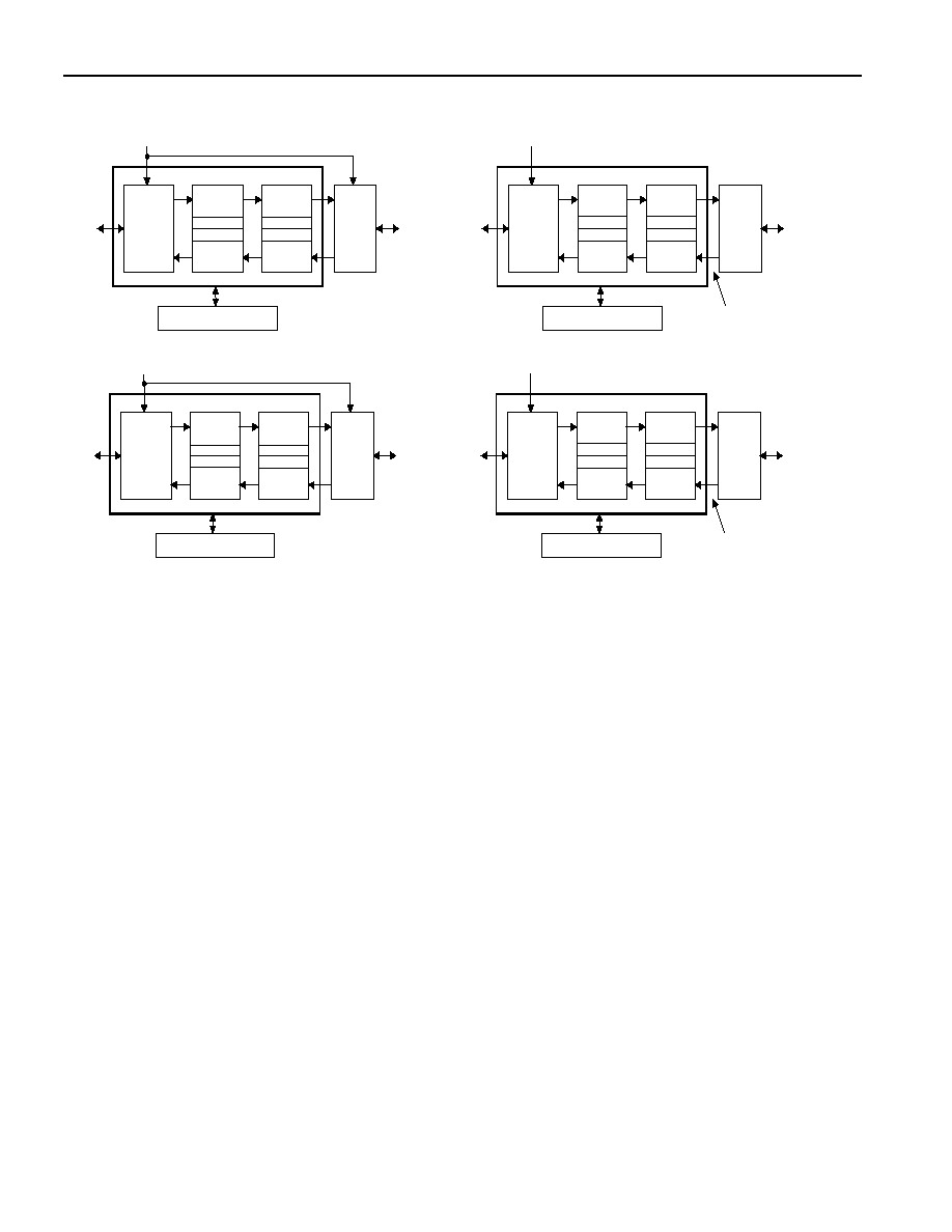
1.2 Typical Applications
1.3 Functional Description
The analog AMI/B8ZS waveform off of the T1 line is transformer coupled into the RRING and RTIP
pins of the DS2196. The device recovers clock and data from the analog signal and passes it through the
optional jitter attenuator to the receive side framer where the digital serial stream is analyzed to locate the
framing/multiframe pattern. The DS2196 contains an active filter that reconstructs the analog received
signal for the nonlinear losses that occur in transmission. The device has a usable receive sensitivity of 0
dB to �36 dB, which allows the device to operate on cables up to 6000 feet in length. The receive side
framer locates D4 (SLC�96) or ESF multiframe boundaries as well as detects incoming alarms including,
carrier loss, loss of synchronization, blue (AIS) and yellow alarms.
The transmit side of the DS2196 is totally independent from the receive side in both the clock
requirements and characteristics. The transmit formatter will provide the necessary frame/multiframe data
overhead for T1 transmission. Once the data stream has been prepared for transmission, it is sent via the
optional jitter attenuator to the wave shaping and line driver functions. The DS2196 will drive the T1 line
from the TTIP and TRING pins via a coupling transformer. The line driver can handle both long haul
(CSU) and short haul (DSX�1) lines.
Long /
Short
Haul
Line
Interface
Unit
(LIU)
Rx
Framer A
Rx HDLC
Tx HDLC
Tx
Formatter A
Rx
Framer B
Rx HDLC
Tx HDLC
Tx
Formatter B
Long /
Short
Haul
Line
Interface
Unit
(LIU)
T1
Interface
A
T1
Interface
B
Microcontroller
DS2196
1.544 MHz
Long /
Short
Haul
Line
Interface
Unit
(LIU)
Rx
Framer A
Rx HDLC
Tx HDLC
Tx
Formatter A
Rx
Framer B
Rx HDLC
Tx HDLC
Tx
Formatter B
T3 /
SONET /
Optical
Mux
T1
Network
Interface
Microcontroller
DS2196
1.544 MHz
NRZ
Interface
OFFICE REPEATER/NIU
Long /
Short
Haul
Line
Interface
Unit
(LIU)
Rx
Framer A
Rx HDLC
Tx HDLC
Tx
Formatter A
Rx
Framer B
Rx HDLC
Tx HDLC
Tx
Formatter B
Short
Haul
Line
Interface
Unit
(LIU)
Telco
T1
Interface
CPE
T1
Interface
Microcontroller
DS2196
1.544 MHz
Long /
Short
Haul
Line
Interface
Unit
(LIU)
Rx
Framer A
Rx HDLC
Tx
Tx
Formatter A
Rx
Framer B
Rx HDLC
Tx HDLC
Tx
Formatter B
HDSL1 /
HDSL2
Modem
T1
Interface
(Remote or
CO Located)
One or Two
Sets of
Twisted
Pair
Microcontroller
DS2196
1.544 MHz
NRZ
Interface
CSU APPLICATION
HDSL1/HDSL2 APPLICATION
T3/SONET/OPTICAL MULTIPLEXER
APPLICATION

DS2196
8 of 157
Reader's Note: This data sheet assumes a particular nomenclature of the T1 operating environment. In
each 125
ms frame, there are 24 8-bit channels plus a framing bit. It is assumed that the framing bit is sent
first followed by channel 1. Each channel is made up of 8 bits that are numbered 1 to 8. Bit number 1 is
the MSB and is transmitted first. Bit number 8 is the LSB and is transmitted last. The following
abbreviations are used throughout this data sheet:
BERT
Bit Error Rate Tester
D4
Superframe (12 frames per multiframe) Multiframe Structure
SLC�96
Subscriber Loop Carrier�96 Channels
ESF
Extended Superframe (24 frames per multiframe) Multiframe Structure
B8ZS
Bipolar with Eight Zero Substitution
CRC
Cyclical Redundancy Check
Ft
Terminal Framing Pattern in D4
Fs
Signaling Framing Pattern in D4
FPS
Framing Pattern in ESF
MF
Multiframe
BOC
Bit-Oriented Code
HDLC
High-Level Data-Link Control
FDL
Facility Data Link

DS2196
9 of 157
Framer Loopback A
Payload Loopback A
AIS & AIS-CI Generation
B8ZS Encode
CRC Generation
Yellow Alarm Generation
Signaling Insertion
Clear Channel
F-Bit Insertion
P
a
ra
ll
el C
o
n
t
ro
l
P
o
rt
(
r
ou
t
e
d t
o
al
l
b
l
ock
s
)
R
ece
ive
S
i
de
Fr
am
er
A
Tr
a
n
s
m
i
t
S
i
d
e
Fo
r
m
a
t
t
e
r
A
BPV Counter
Alarm Detection
Loop Code Generation
fs
y
n
c
da
t
a
clo
c
k
ms
y
n
c
da
t
a
cl
ock
D0 to D7 /
AD0 to AD7
BTS
INT*
TSYNCA
TCLKA
TCHCLKA/
TLCLKA
TSERA
TCHBLKA/
TLINKA
WR*(R/W*)
RD*(DS*)
RCHCLKA/
RLCLKA
CS*
RCHBLKA/
RLINKA
RMSYNCA
RSERA
RFSYNCA
FDL
E
x
t
r
a
c
t
i
o
n
FD
L I
n
s
e
r
t
i
o
n
B8ZS Decoder
Synchronizer
Loop Code Detector
CRC/Frame Error Count
Signaling Extraction
Channel Marking
RLOSA / LOTCA
ALE(AS) / A7
A0 to A6
MUX
8
RCL
Line Drivers
CSU Filters
Wave Shaping
Local Loopback
TR
I
N
G
TT
I
P
Jitter Attenuation
(can be placed in either transmit or receive path)
Filter
Peak Detect
Clock / Data
Recovery
RR
I
N
G
RT
I
P
Remote Loopback
VCO /
PLL
MC
L
K
1.
54
4 M
H
z
LIU AIS Generation
RCLKA
7
RPOSLO
RNEGLO
RNEGIA
RPOSIA
TPOSLI
TNEGLI
TNEGOA/
TFSYNCA
TPOSOA/
TNRZA
RCLKLO
RCLKIA
Per-Channel Loopback
TCLKLI
TCLKOA
64
-
B
yt
e
B
u
f
f
er
BO
M
D
e
t
e
c
t
i
o
n
64
-
B
yt
e
B
u
f
f
er
B
O
M
G
e
n
e
ra
tio
n
m
u
x
(
c
on
t
r
ol
l
e
d
vi
a
C
C
R
4
A
.
2)
m
u
x
(c
o
n
tro
lle
d
vi
a
C
C
R
4
A
.
2)
ms
y
n
c
fs
y
n
c
Framer Loopback B
AIS & AIS-CI Generation
B8ZS Encode
CRC Generation
Yellow Alarm Generation
Signaling Insertion
Clear Channel
F-Bit Insertion
Tr
a
n
s
m
i
t
S
i
d
e
Fo
r
m
a
t
t
e
r
B
BPV Counter
Alarm Detection
Loop Code Generation
fs
y
n
c
da
ta
cl
ock
ms
y
n
c
da
t
a
cl
o
c
k
FD
L E
x
t
r
a
c
t
i
o
n
FDL
I
n
s
e
r
t
i
o
n
B8ZS Decoder
Synchronizer
Loop Code Detector
CRC/Frame Error Count
Signaling Extraction
Channel Marking
Per-Channel Loopback
64
-
B
yt
e
B
u
f
f
er
B
O
M
D
e
te
ct
io
n
64
-
B
yt
e
B
u
f
f
er
BOM
Ge
n
e
r
a
t
i
o
n
ms
y
n
c
fs
y
n
c
TS
YNC
Co
n
t
r
o
l
T
S
YNC
Co
n
t
r
o
l
Cl
o
c
k
Ge
n
Cl
o
c
k
Ge
n
Cl
o
c
k
Ge
n
TSYNCB
TCLKB
TSERB
TCHCLKB
TLCLKB
TCHBLKB/
TLINKB
RLOSB / LOTCB
RCHCLKB/
RLCLKB
RCHBLKB/
RLINKB
RCLKB
RMSYNCB
RSERB
RFSYNCB
LI
U
AI
S
PRO-
TEC
T
WO
R
K
-
IN
G
WPS
WN
R
Z
WC
L
K
PNRZ
PCLK
TN
E
G
o
r
TF
S
Y
N
C
TCL
K
TP
O
S
o
r
T
N
R
Z
L
FSYNC
LCL
K
LN
R
Z
m
u
x (
c
o
n
t
r
ol
l
e
d
v
i
a
C
C
R4
B.
2
)
RPOS
I
B
RNEG
I
B
RC
L
K
I
B
T
P
OS
OB
/
TN
R
Z
B
TC
L
K
O
B
TN
E
G
O
B
/
T
FSY
NC
B
R
ece
ive
S
i
de
Fr
am
er
B
Cl
o
c
k
Ge
n
To
BE
R
T
Mu
x
JT
A
G
JTCLK
JTMS
JTDO
JTDI
JTRST*
To
BE
R
T
Mu
x
Insert Data From BERT
Insert Data From BERT
POWER
DVSS
(
3
)
RVSS
(
2
)
T
VDD
TV
S
S
RVDD
DVDD
(
3
)
BE
R
T
M
u
x
RXA
RXB
TX
A
4
4
5
To /
Fr
om
BE
R
T
M
u
x
RBPVA
RBPVB
Da
t
a
So
u
r
c
e
M
UX C
o
n
t
r
o
l
(
c
o
n
tro
l
le
d
v
i
a
CC
R1
A
.
2
/
3
/
4
)
Back End Loopback
RSER
RMSYNC
RCLK
SYSCLK
SSER
SFSYNC
D
S
21
75
(o
p
tio
n
a
l)
f
r
om
R
e
cei
ve
F
r
am
er
B
(o
n
l
y
in
F
T
1
ap
p
lic
at
io
n
)
ms
y
n
c
1.
54
4M
H
z
RC
L
K
B
RM
SYN
C
B
Us
e
r
Ou
t
p
u
t
Por
t
(
4
pi
n
s
)
UOP0
UOP1
UOP2
UOP3
FL
B
B
2
FLB B Mux
F
r
o
m
BERT
M
u
x
LO
T
C
M
u
x
Fr
om
MC
L
K
4
4
BE
R
T
clock
data
clock
data
Corrupt F-Bit / Payload
Corrupt F-Bit / Payload
sync
Payload Loopback B
mu
x
(
c
o
n
t
r
o
l
l
e
d
v
i
a
C
CR4
B.
2
)
LOTC
M
u
x
Fr
om
MC
L
K
LN
R
Z
A
I
S
G
e
ner
a
t
i
on
Figure 1-1. T1 Dual Framer LIU

DS2196
10 of 157
2. PIN DESCRIPTION
Table 2-1. Pin Description Sorted by Pin Number
PIN
SYMBOL
TYPE
FUNCTION
1
PCLK
I
Protect Clock Input.
2
PNRZ
I
Protect NRZ Data Input.
3
WCLK
I
Working Clock Input.
4
WNRZ
I
Working NRZ Data Input.
5
JTMS
I
IEEE 1149.1 Test Mode Select.
6
JTCLK
I
IEEE 1149.1 Test Clock Signal.
7
JTRST*
I
IEEE 1149.1 Test Reset.
8
JTDI
I
IEEE 1149.1 Test Data Input.
9
JTDO
O
IEEE 1149.1 Test Data Output.
10
RCL
O
Receive LIU Carrier Loss.
11
LNRZ
O
LIU NRZ & Positive Data Output.
12
LCLK
O
LIU Clock Output.
13
LFSYNC
O
LIU Frame Sync Pulse & Negative Data Output.
14
RPOSLO
O
Receive Positive & NRZ Data Output from the LIU.
15
RNEGLO
O
Receive Negative & NRZ Data Output from the LIU.
16
RCLKLO
O
Receive Clock Output from the LIU.
17
BTS
I
Bus Type Select. 0 = Intel / 1 = Motorola.
18
RTIP
I
Receive Analog Tip Input.
19
RRING
I
Receive Analog Ring Input.
20
RVDD
�
Receive Analog Positive Supply. 3.3V (�5%).
21
RVSS
�
Receive Analog Signal Ground.
22
INT*
O
Interrupt. Open Drain. Active Low Signal.
23
RVSS
�
Receive Analog Signal Ground.
24
MCLK
I
Master Clock Input. 1.544 MHz (�50 ppm).
25
UOP3
O
User Defined Output Port Bit 3.
26
UOP2
O
User Defined Output Port Bit 2.
27
UOP1
O
User Defined Output Port Bit 1.
28
UOP0
O
User Defined Output Port Bit 0.
29
TTIP
O
Transmit Analog Tip Output.
30
TVSS
�
Transmit Analog Signal Ground.
31
TVDD
�
Transmit Analog Positive Supply. 3.3V (�5%).
32
TRING
O
Transmit Analog Ring Output.
33
TPOSLI
I
Transmit Positive & NRZ Data for the LIU.
34
TNEGLI
I
Transmit Negative & NRZ Data for the LIU.
35
TCLKLI
I
Transmit Clock Input for the LIU.
36
TCHBLKB/
TLINKB
I/O
Transmit Channel Blocking Clock Output from Formatter B /
Transmit FDL Link Data Input for Formatter B.
37
TCHCLKB/
TLCLKB
O
Transmit DS0 Channel Clock Output from Formatter B /
Transmit FDL Link Clock Output from Formatter B.
38
TSYNCB
I/O
Transmit Frame & Multiframe Pulse for/from Formatter B.
39
TCLKB
I
Transmit Clock Input for Formatter B.
40
TSERB
I
Transmit Serial Data Input for Formatter B.
41
TPOSOB/
TNRZB
O
Transmit Positive Data Output from Formatter B /
Transmit NRZ Data Output from Formatter B.
42
TNEGOB /
TFSYNCB
O
Transmit Negative Data Output from Formatter B /
Transmit Frame Sync Pulse Output from Formatter B.

DS2196
11 of 157
PIN
SYMBOL
TYPE
FUNCTION
43
TCLKOB
O
Transmit Clock Output from Formatter B.
44
DVSS
�
Digital Signal Ground.
45
DVDD
�
Digital Positive Supply. 3.3V (�5%).
46
TCLKOA
O
Transmit Clock Output from Formatter A.
47
TNEGOA /
TFSYNCA
O
Transmit Negative Data Output from Formatter A /
Transmit Frame Sync Pulse Output from Formatter A.
48
TPOSOA /
TNRZA
O
Transmit Positive Data Output / Transmit NRZ Data Output from
Formatter A.
49
TSERA
I
Transmit Serial Data Input for Formatter A.
50
TCLKA
I
Transmit Clock Input for Formatter A.
51
TSYNCA
I/O
Transmit Frame & Multiframe Pulse for/from Formatter A.
52
TCHCLKA /
TLCLKA
O
Transmit DS0 Channel Clock Output from Formatter A /
Transmit FDL Link Clock Output from Formatter A.
53
TCHBLKA /
TLINKA
I/O
Transmit Channel Blocking Clock Output from Formatter A /
Transmit FDL Link Data Input for Formatter A.
54
MUX
I
Bus Operation. 0 = Non-Mux Bus / 1 = Mux Bus Operation.
55
D0 / AD0
I/O
Data Bus Bit 0 / Address/Data Bus Bit 0. LSB.
56
D1 / AD1
I/O
Data Bus Bit 1 / Address/Data Bus Bit 1.
57
D2 / AD2
I/O
Data Bus Bit 2 / Address/Data Bus Bit 2.
58
D3 / AD3
I/O
Data Bus Bit 3 / Address/Data Bus Bit 3.
59
D4 / AD4
I/O
Data Bus Bit 4 / Address/Data Bus Bit 4.
60
D5 / AD5
I/O
Data Bus Bit 5 / Address/Data Bus Bit 5.
61
D6 / AD6
I/O
Data Bus Bit 6 / Address/Data Bus Bit 6.
62
D7 / AD7
I/O
Data Bus Bit 7 / Address/Data Bus Bit 7. MSB.
63
DVSS
�
I/O Digital Signal Ground.
64
DVDD
�
I/O Digital Positive Supply. 3.3V (�5%).
65
A0
I
Address Bus Bit 0. LSB.
66
A1
I
Address Bus Bit 1
67
A2
I
Address Bus Bit 2
68
A3
I
Address Bus Bit 3
69
A4
I
Address Bus Bit 4
70
A5
I
Address Bus Bit 5
71
A6
I
Address Bus Bit 6
72
A7 / ALE(AS)
I
Address Bus Bit 7 / Address Latch Enable (Address Strobe). MSB.
73
RD*(DS*)
I
Read Input (Data Strobe).
74
CS*
I
Chip Select. Active Low Signal.
75
WR*(R/W*)
I
Write Input (Read/Write).
76
RCHBLKA /
RLINKA
O
Receive Channel Blocking Clock Output from Framer A /
Receive FDL Link Data Output from Framer A.
77
RCHCLKA /
RLCLKA
O
Receive DS0 Channel Clock Output from Framer A /
Receive FDL Link Clock Output from Framer A.
78
RCLKIA
I
Receive Clock Input for Framer A.
79
RPOSIA
I
Receive Positive & NRZ Data Input for Framer A.
80
RNEGIA
I
Receive Negative & NRZ Data Input for Framer A.
81
RCLKA
O
Receive Clock Output from Framer A.
82
RSERA
O
Receive Serial Data Output from Framer A.
83
RMSYNCA
O
Receive Multiframe Pulse from Framer A.
84
RFSYNCA
O
Receive Frame Pulse from Framer A.
85
RLOSA/
LOTCA
O
Receive Loss Of Synchronization from Framer A /
Loss of Transmit Clock Framer A.

DS2196
12 of 157
PIN
SYMBOL
TYPE
FUNCTION
86
RBPVA
O
Receive bipolar Violation (BPV) from Framer A.
87
DVSS
�
Digital Signal Ground.
88
DVDD
�
Digital Positive Supply. 3.3V (�5%).
89
RBPVB
O
Receive bipolar Violation (BPV) from Framer B.
90
RLOSB/
LOTCB
O
Receive Loss Of Synchronization from Framer B /
Loss of Transmit Clock Framer B.
91
RFSYNCB
O
Receive Frame Pulse from Framer B.
92
RMSYNCB
O
Receive Multiframe Pulse from Framer B.
93
RSERB
O
Receive Serial Data Output from Framer B.
94
RCLKB
O
Receive Clock Output from Framer B.
95
RNEGIB
I
Receive Negative & NRZ Data Input for Framer B.
96
RPOSIB
I
Receive Positive & NRZ Data Input for Framer B.
97
RCLKIB
I
Receive Clock Input for Framer B.
98
RCHCLKB /
RLCLKB
O
Receive DS0 Channel Clock Output from Framer B /
Receive FDL Link Clock Output from Framer B.
99
RCHBLKB /
RLINKB
O
Receive Channel Blocking Clock Output from Framer B /
Receive FDL Link Data Output from Framer B.
100
WPS
I
Working/Protect Select.

DS2196
13 of 157
3. PIN FUNCTION DESCRIPTION
Transmit Side Pins
Signal Name:
TCLKA/B
Signal Description:
Transmit Clock
Signal Type:
Input
A 1.544 MHz primary clock is applied here. Used to clock data through the transmit side formatters. TCLKA/B
can be internally connected to RCLKB/A via the CCR4B.2 control bit.
Signal Name:
TSERA/B
Signal Description:
Transmit Serial Data
Signal Type:
Input
Transmit NRZ serial data. Sampled on the falling edge of TCLKA or TCLKB. TSERA/B can be internally
connected to RSERB/A via the CCR4B.2 control bit.
Signal Name:
TSYNCA/B
Signal Description:
Transmit Sync
Signal Type:
Input / Output
When programmed as an input, a pulse at this pin will establish either frame or multiframe boundaries for the
transmit side. Via TCR2A.2 and TCR2B.2, the DS2196 can be programmed to output either a frame or multiframe
pulse at this pin. If this pin is set to output pulses at frame boundaries, it can also be set via TCR2A.4 and
TCR2B.4 to output double�wide pulses at signaling frames. See Section 21 for details. TSYNCA/B can be
internally connected to RMSYNCB/A via the CCR4B.2 control bit.
Signal Name:
TCHCLKA/B / TLCLKA/B
Signal Description:
Transmit Channel Clock / Transmit Link Clock
Signal Type:
Output
A dual function pin depending on the setting of the CCR4A.1 and CCR4B.1 control bits. If TCHCLK is selected, a
192-kHz clock, which pulses high during the LSB of each channel, will be output. If TLCLK is selected, either a 4
kHz or 2 kHz (ZBTSI) demand clock for the TLINK data is output. This output signal is always synchronous with
TCLKA or TCLKB. See Section 21 for details.
Signal Name:
TCHBLKA/B / TLINKA/B
Signal Description:
Transmit Channel Block / Transmit Link Data
Signal Type:
Input / Output
A dual function pin depending on the setting of the CCR4A.1 and CCR4B.1 control bits. If TCHBLK is selected, a
user programmable output that can be forced high or low during any of the 24 T1 channels is output. Useful for
blocking clocks to a serial UART or LAPD controller in applications where not all T1 channels are used such as
Fractional T1, 384 kbps service, 768 kbps, or ISDN�PRI. Also useful for locating individual channels in drop�
and�insert applications, for external per�channel loopback, and for per�channel conditioning. See Section 21 for
details. If TLINK is selected, this pin will be sampled on the falling edge of TCLKA or TCLKB for data insertion
into either the FDL stream (ESF) or the Fs�bit position (D4) or the Z�bit position (ZBTSI). See Section 21 for
details. This signal is always synchronous with TCLKA or TCLKB.
Signal Name:
TPOSOA/B / TNRZA/B
Signal Description:
Transmit Positive & NRZ Data Output
Signal Type:
Output
Updated on the rising edge of TCLKOA and rising or falling edge of TCLKOB with either bipolar data or NRZ
data out of the transmit side formatter. This pin can be programmed to source NRZ data via the Output Data
Format (CCR1A.6 and CCR1B.6) control bits.

DS2196
14 of 157
Signal Name:
TNEGA/B / TFSYNCA/B
Signal Description:
Transmit Negative Data & Frame Sync Pulse Output
Signal Type:
Output
Updated on the rising edge of TCLKA or TCLKB with either bipolar data or a frame sync pulse out of the transmit
side formatter. This pin can be programmed to source the frame sync pulse via the Output Data Format (CCR1A.6
and CCR1B.6) control bits.
Receive Framer Pins
Signal Name:
RCHCLKA/B / RLCLKA/B
Signal Description:
Receive Channel Clock / Receive Link Clock
Signal Type:
Output
A dual function pin depending on the setting of the CCR4A.1 and CCR4B.1 control bits. If RCHCLK is selected, a
192-kHz clock, which pulses high during the LSB of each channel, will be output. If RLCLK is selected, either a 4
kHz or 2 kHz (ZBTSI) clock for the RLINK data is output. This output signal is always synchronous with RCLKA
or RCLKB.
Signal Name:
RCHBLKA/B / RLINKA/B
Signal Description:
Receive Channel Block / Receive Link Data
Signal Type:
Output
A dual function pin depending on the setting of the CCR4A.1 and CCR4B.1 control bits. If RCHBLK is selected, a
user programmable output that can be forced high or low during any of the 24 T1 channels. Useful for blocking
clocks to a serial UART or LAPD controller in applications where not all T1 channels are used such as Fractional
T1, 384 kbps service, 768 kbps, or ISDN�PRI. Also useful for locating individual channels in drop�and�insert
applications, for external per�channel loopback, and for per�channel conditioning. See Section 21 for details. If
RLINK is selected, then either FDL data (ESF) or Fs bits (D4) or Z bits (ZBTSI) one RCLKA before the start of a
frame are output. See Section 21 for details. This signal is always synchronous with RCLKA or RCLKB.
Signal Name:
RSERA/B
Signal Description:
Receive Serial Data
Signal Type:
Output
Received NRZ serial data. Updated on rising edges of RCLKA or RCLKB.
Signal Name:
RFSYNCA/B
Signal Description:
Receive Frame Sync
Signal Type:
Output
An extracted pulse, one RCLKA or RCLKB wide, is output at this pin which identifies frame boundaries. Via
RCR2A.5 and RCR2B.5, RFSYNC can also be set to output double�wide pulses on signaling frames. This signal
is always synchronous with RCLKA or RCLKB
.
Signal Name:
RMSYNCA/B
Signal Description:
Receive Multiframe Sync
Signal Type:
Output
An extracted pulse, one RCLKA or RCLKB wide, is output at this pin which identifies multiframe boundaries.
This signal is always synchronous with RCLKA or RCLKB.

DS2196
15 of 157
Signal Name:
RLOSA/B / LOTCA/B
Signal Description:
Receive Loss of Sync / Loss of Transmit Clock
Signal Type:
Output
A dual function output that is controlled by the CCR3.5 control bit. This pin can be programmed to either toggle
high when the synchronizer is searching for the frame and multiframe or to toggle high if the TCLK pin has not
been toggled for 5
msec.
Signal Name:
RBPVA/B
Signal Description:
Receive BPV
Signal Type:
Output
This pin will toggle high for one RCLKA or RCLKB clock cycle for each bipolar Violation (BPV) detected by the
framer.
Signal Name:
RPOSIA/B
Signal Description:
Receive Positive Data Input
Signal Type:
Input
Sampled on the falling edge of RCLKIA and either rising or falling edge of RCLKIB for data to be clocked
through the receive side framer. RPOSIA
/B and RNEGIA/B can be tied together for a NRZ interface.
RPOSIA be internally connected to RPOSLO via the CCR4A.2 control bit.
Signal Name:
RNEGIA/B
Signal Description:
Receive Negative Data Input
Signal Type:
Input
Sampled on the falling edge of RCLKI for data to be clocked through the receive side framer. RPOSIA/B and
RNEGIA/B can be tied together for a NRZ interface. RNEGIA be internally connected to RNEGLO via the
CCR4A.2 control bit.
Signal Name:
RCLKIA/B
Signal Description:
Receive Clock Input
Signal Type:
Input
Signal used to clock data through the receive side framers. RCLKIA can be internally connected to RCLKLO via
the CCR4A.2 control bit.
User Port Pins
Signal Name:
UOP0/1/2/3
Signal Description:
User Output Port
Signal Type:
Output
These output port pins can be set low or high via the CCR7B.0 to CCR7B.3 control bits. The pins are forced low
on power-up.

DS2196
16 of 157
Parallel Control Port Pins
Signal Name:
INT*
Signal Description:
Interrupt
Signal Type:
Output
Flags host controller during conditions and change of states as defined in the Status Registers. Active low, open
drain output.
Signal Name:
MUX
Signal Description:
Bus Operation
Signal Type:
Input
Set low to select non-multiplexed bus operation. Set high to select multiplexed bus operation.
Signal Name:
D0 to D7 / AD0 to AD7
Signal Description:
Data Bus or Address/Data Bus
Signal Type:
Input / Output
In non-multiplexed bus operation (MUX = 0), serves as the data bus. In multiplexed bus operation (MUX = 1),
serves as a 8�bit multiplexed address / data bus.
Signal Name:
A0 to A6
Signal Description:
Address Bus
Signal Type:
Input
In non-multiplexed bus operation (MUX = 0), serves as the address bus. In multiplexed bus operation (MUX = 1),
these pins are not used and should be tied low.
Signal Name:
BTS
Signal Description:
Bus Type Select
Signal Type:
Input
Strap high to select Motorola bus timing; strap low to select Intel bus timing. This pin controls the function of the
RD*(DS*), ALE (AS), and WR*(R/W*) pins. If BTS = 1, then these pins assume the function listed in parenthesis
().
Signal Name:
RD* (DS*)
Signal Description:
Read Input (Data Strobe)
Signal Type:
Input
RD* is an active low signal. DS* polarity is determined by the MUX pin setting. Refer to section 21 for details.
Signal Name:
CS*
Signal Description:
Chip Select
Signal Type:
Input
Must be low to read or write to the device. CS* is an active low signal.
Signal Name:
ALE(AS) / A7
Signal Description:
A7 or Address Latch Enable (Address Strobe)
Signal Type:
Input
In non-multiplexed bus operation (MUX = 0), serves as the upper address bit. In multiplexed bus operation (MUX
= 1), serves to demultiplex the bus on a positive�going edge.
Signal Name:
WR*( R/W*)
Signal Description:
Write Input (Read/Write)
Signal Type:
Input
WR* is an active low signal.

DS2196
17 of 157
Signal Name:
JTCLK
Signal Description:
JTAG IEEE 1149.1 Test Serial Clock
Signal Type:
Input
This signal is used to shift data into JTDI on the rising edge and out of JTDO on the falling edge. If not used, this
pin should be pulled high.
Signal Name:
JTDI
Signal Description:
JTAG IEEE 1149.1 Test Serial Data Input
Signal Type:
Input
Test instructions and data are clocked into this signal on the rising edge of JTCLK. If not used, this pin should be
pulled high. This pin has an internal pull-up.
Signal Name:
JTDO
Signal Description:
JTAG IEEE 1149.1 Test Serial Data Output
Signal Type:
Output
Test instructions are clocked out of this signal on the falling edge of JTCLK. If not used, this pin should be left
open circuited.
Signal Name:
JTRST*
Signal Description:
JTAG IEEE 1149.1 Test Reset
Signal Type:
Input
This signal is used to synchronously reset the test access port controller. At power up, JTRST must be set low and
then high. This action will set the device into the boundary scan bypass mode allowing normal device operation.
If boundary scan is not used, this pin should be held low. This pin has an internal pull-up.
Signal Name:
JTMS
Signal Description:
JTAG IEEE 1149.1 Test Mode Select
Signal Type:
Input
This signal is sampled on the rising edge of JTCLK and is used to place the test port into the various defined IEEE
1149.1 states. If not used, this pin should be pulled high. This signal has an internal pull-up.
Line Interface Pins
Signal Name:
MCLK
Signal Description:
Master Clock Input
Signal Type:
Input
A 1.544 MHz (�50 ppm) clock source with TTL levels is applied at this pin. This clock is used internally for both
clock/data recovery and for jitter attenuation. This clock is also used to source AIS within the LIU.
Signal Name:
RTIP & RRING
Signal Description:
Receive Tip and Ring
Signal Type:
Input
Analog inputs for clock recovery circuitry. These pins connect via a 1:1 transformer to the T1 line. See Section 19
for details.
Signal Name:
TTIP & TRING
Signal Description:
Transmit Tip and Ring
Signal Type:
Output
Analog line driver outputs. These pins connect via a 1:2 step�up transformer to the T1 line. See Section 19 for
details.
Signal Name:
LFSYNC
Signal Description:
LIU Frame Sync

DS2196
18 of 157
Signal Type:
Output
This digital output will provide either a frame synchronization pulse or the negative half of a bipolar data stream.
The signal is based on what is provided at the TNEGLI input.
Signal Name:
LNRZ
Signal Description:
LIU NRZ Data
Signal Type:
Output
This digital output will provide either a NRZ data stream or the positive half of a bipolar data stream. The signal is
based on what is provided at the TPOSLI input.
Signal Name:
LCLK
Signal Description:
LIU Clock
Signal Type:
Output
This digital output provides the 1.544 MHz transmit LIU clock. The signal is based on what is provided at the
TCLKLI input.
Signal Name:
TNEGLI
Signal Description:
Transmit Negative Data for the LIU
Signal Type:
Input
This digital input is used to pass either the negative half of a bipolar data stream or a frame synchronization pulse
via the jitter attenuator block to the transmit line driver block and the LFSYNC output pin. Data input to this pin is
sampled on the falling edge of TCLKLI. TNEGLI can be internally connected to TNEGOA/TFSYNCA via the
CCR4A.2 control bit.
Signal Name:
TPOSLI
Signal Description:
Transmit Positive Data for the LIU
Signal Type:
Input
This digital input is used to pass either the positive half of a bipolar data stream or a NRZ data stream via the jitter
attenuator block to the transmit line driver block and the LNRZ output pin. Data input to this pin is sampled on the
falling edge of TCLKLI. TPOSLI can be internally connected to TPOSOA/TNRZA via the CCR4A.2 control bit.
Signal Name:
TCLKLI
Signal Description:
Transmit Clock for the LIU
Signal Type:
Input
This digital input is used to pass a 1.544 MHz clock via the jitter attenuator block to the transmit line driver block
and the LCLK output pin. TCLKLI can be internally connected to TCLKOA via the CCR4A.2 control bit.
Signal Name:
WNRZ
Signal Description:
Working NRZ Data
Signal Type:
Input
This digital input is used to pass a NRZ data stream via the Data Source Selection MUX and the jitter attenuator
block to the RPOSLO and RNEGLO output pins. Data input to this pin is sampled on the falling or rising edge of
WCLK.
Signal Name:
WCLK
Signal Description:
Working Clock
Signal Type:
Input
This digital input is used to pass a 1.544 MHz clock via the Data Source Selection MUX and the jitter attenuator
block to the RCLKLO output pin.

DS2196
19 of 157
Signal Name:
PNRZ
Signal Description:
Protect NRZ Data
Signal Type:
Input
This digital input is used to pass a NRZ data stream via the Data Source Selection MUX and the jitter attenuator
block to the RPOSLO and RNEGLO output pins. Data input to this pin is sampled on the falling or rising edge of
PCLK.
Signal Name:
PCLK
Signal Description:
Protect Clock
Signal Type:
Input
This digital input is used to pass a 1.544 MHz clock via the Data Source Selection MUX and the jitter attenuator
block to the RCLKLO output pin.
Signal Name:
RCL
Signal Description:
Receive Carrier Loss
Signal Type:
Output
Set high when the line interface (LIU) detects a carrier loss.
Signal Name:
RPOSLO
Signal Description:
Receive Positive Data Output from the LIU
Signal Type:
Output
Updated on the rising edge of RCLKLO with either bipolar data out of the LIU or NRZ data from the WNRZ or
PNRZ inputs.
Signal Name:
RNEGLO
Signal Description:
Receive Negative Data Output from the LIU
Signal Type:
Output
Updated on the rising edge of RCLKLO with either bipolar data out of the LIU or NRZ data from the WNRZ or
PNRZ inputs.
Signal Name:
RCLKO
Signal Description:
Receive Clock Output
Signal Type:
Output
Either a buffered recovered clock from the T1 line or the clock provided at the WCLK or PCLK inputs.
Signal Name:
WPS
Signal Description:
Working or Protect Select
Signal Type:
Input
This digital input can be used to select between the WNRZ/WCLK (working) or PNRZ/PCLK (protect) data
inputs. For this pin to be active the Data Source MUX must be properly configured via the CCR1A.2, CCR1A.3,
and CCR1A.4 control bits.

DS2196
20 of 157
Supply Pins
Signal Name:
DVDD
Signal Description:
Digital Positive Supply
Signal Type:
Supply
3.3 volts �5%. Should be tied to the RVDD and TVDD pins.
Signal Name:
RVDD
Signal Description:
Receive Analog Positive Supply
Signal Type:
Supply
3.3 volts �5%. Should be tied to the DVDD and TVDD pins.
Signal Name:
TVDD
Signal Description:
Transmit Analog Positive Supply
Signal Type:
Supply
3.3 volts �5%. Should be tied to the RVDD and DVDD pins.
Signal Name:
DVSS
Signal Description:
Digital Signal Ground
Signal Type:
Supply
Should be tied to the RVSS and TVSS pins.
Signal Name:
RVSS
Signal Description:
Receive Analog Signal Ground
Signal Type:
Supply
0.0 volts. Should be tied to the DVSS and TVSS pins.
Signal Name:
TVSS
Signal Description:
Transmit Analog Ground
Signal Type:
Supply
0.0 volts. Should be tied to the DVSS and TVSS pins.

DS2196
21 of 157
4. REGISTER MAP
Table 4-1. Register Map Sorted By Address
ADDRESS
R/W
REGISTER NAME
REGISTER
ABBREVIATION
00
R/W
HDLC Control for Framer A
HCRA
01
R/W
HDLC Status from Framer A
HSRA
02
R/W
HDLC Interrupt Mask for Framer A
HIMRA
03
R/W
Receive HDLC Information for Framer A
RHIRA
04
R/W
Receive Bit Oriented Code for Framer A
RBOCA
05
R
Receive HDLC FIFO from Framer A
RHFA
06
R/W
Transmit HDLC Information for Formatter A
THIRA
07
R/W
Transmit Bit Oriented Code for Formatter A
TBOCA
08
W
Transmit HDLC FIFO for Formatter A
THFA
09
R/W
Test 2 for Framer A (Set to 00h on power-up)
--
0A
R/W
Common Control 7 for Framer A
CCR7A
0B
--
Reserved (Set to 00h on power-up)
--
0C
--
Reserved (Set to 00h on power-up)
--
0D
--
Reserved (Set to 00h on power-up)
--
0E
R
Interrupt Status Register
ISR
0F
R
Device ID
IDR
10
R/W
Receive Information 3 from Framer A
RIR3A
11
R/W
Common Control 4 for Framer A
CCR4A
12
R/W
In�Band Code Control for Framer A
IBCCA
13
R/W
Transmit Code Definition 1 for Framer A
TCD1A
14
R/W
Receive Up Code Definition 1 for Framer A
RUPCD1A
15
R/W
Receive Down Code Definition 1 for Framer A
RDNCD1A
16
R/W
Transmit Code Definition 2 for Framer A
TCD2A
17
R/W
Receive Up Code Definition 2 for Framer A
RUPCD2A
18
R/W
Receive Down Code Definition 2 for Framer A
RDNCD2A
19
R/W
Common Control 5 for Framer A
CCR5A
1A
R
Transmit DS0 Monitor for Framer A
TDS0MA
1B
R/W
Receive Spare Code Definition 1 for Framer A
RSCD1A
1C
R/W
Receive Spare Code Definition 2 for Framer A
RSCD2A
1D
R/w
Receive Spare Code Control for Framer A
RSCCA
1E
R/W
Common Control 6 for Framer A
CCR6A
1F
R
Receive DS0 Monitor from Framer A
RDS0MA
20
R/W
Status 1 from Framer A
SR1A
21
R/W
Status 2 from Framer A
SR2A
22
R/W
Receive Information 1 from Framer A
RIR1A
23
R
Line Code Violation Count 1 from Framer A
LCVCR1A
24
R
Line Code Violation Count 2 from Framer A
LCVCR2A
25
R
Path Code Violation Count 1 from Framer A
Multiframe Out of Sync Count 1 from Framer A
PCVCR1A
MOSCR1A
26
R
Path Code violation Count 2 from Framer A
PCVCR2A
27
R
Multiframe Out of Sync Count 2 from Framer A
MOSCR2A
28
R
Receive FDL Register from Framer A
RFDLA
29
R/W
Receive FDL Match 1 for Framer A
RMTCH1A
2A
R/W
Receive FDL Match 2 for Framer A
RMTCH2A
2B
R/W
Receive Control 1 for Framer A
RCR1A

DS2196
22 of 157
ADDRESS
R/W
REGISTER NAME
REGISTER
ABBREVIATION
2C
R/W
Receive Control 2 for Framer A
RCR2A
2D
R/W
Receive Mark 1 for Framer A
RMR1A
2E
R/W
Receive Mark 2 for Framer A
RMR2A
2F
R/W
Receive Mark 3 for Framer A
RMR3A
30
R/W
Common Control 3 for Framer A
CCR3A
31
R/W
Receive Information 2 for Framer A
RIR2A
32
R/W
Transmit Channel Blocking 1 for Formatter A
TCBR1A
33
R/W
Transmit Channel blocking 2 for Formatter A
TCBR2A
34
R/W
Transmit Channel Blocking 3 for Formatter A
TCBR3A
35
R/W
Transmit Control 1 for Formatter A
TCR1A
36
R/W
Transmit Control 2 for Formatter A
TCR2A
37
R/W
Common Control 1 for Framer A
CCR1A
38
R/W
Common Control 2 for Framer A
CCR2A
39
R/W
Transmit Transparency 1 for Formatter A
TTR1A
3A
R/W
Transmit Transparency 2 for Formatter A
TTR2A
3B
R/W
Transmit Transparency 3 for Formatter A
TTR3A
3C
R/W
Transmit Idle 1 for Formatter A
TIR1A
3D
R/W
Transmit Idle 2 for Formatter A
TIR2A
3E
R/W
Transmit Idle 3 for Formatter A
TIR3A
3F
R/W
Transmit Idle Definition for Formatter A
TIDRA
40
R/W
BERT Control Register 0
BC0
41
R/W
BERT Control Register 1
BC1
42
R/W
BERT Control Register 2
BC2
43
R
BERT Information Register
BIR
44
R/W
BERT Alternating Word Count
BAWC
45
R/W
BERT Repetitive Pattern Set Register 0
BRP0
46
R/W
BERT Repetitive Pattern Set Register 1
BRP1
47
R/W
BERT Repetitive Pattern Set Register 2
BRP2
48
R/W
BERT Repetitive Pattern Set Register 3
BRP3
49
R
BERT Bit Count Register 0
BBC0
4A
R
BERT Bit Count Register 1
BBC1
4B
R
BERT Bit Count Register 2
BBC2
4C
R
BERT Bit Count Register 3
BBC3
4D
R
BERT Bit Error Count Register 0
BEC0
4E
R
BERT Bit Error Count Register 1
BEC1
4F
R
BERT Bit Error Count Register 2
BEC2
50
R/W
BERT Interface Control
BIC
51
--
Reserved (Set to 00h on power-up)
--
52
--
Reserved (Set to 00h on power-up)
--
53
--
Reserved (Set to 00h on power-up)
--
54
--
Reserved (Set to 00h on power-up)
--
55
--
Reserved (Set to 00h on power-up)
--
56
--
Reserved (Set to 00h on power-up)
--
57
--
Reserved (Set to 00h on power-up)
--
58
--
Reserved (Set to 00h on power-up)
--
59
--
Reserved (Set to 00h on power-up)
--
5A
--
Reserved (Set to 00h on power-up)
--
5B
--
Reserved (Set to 00h on power-up)
--
5C
--
Reserved (Set to 00h on power-up)
--

DS2196
23 of 157
ADDRESS
R/W
REGISTER NAME
REGISTER
ABBREVIATION
5D
--
Reserved (Set to 00h on power-up)
--
5E
R/W
LIU Test Register 1 (Set to 00h on power-up)
--
5F
R/W
LIU Test Register 2 (Set to 00h on power-up)
--
60
R
Receive Signaling 1 from Framer A
RS1A
61
R
Receive Signaling 2 from Framer A
RS2A
62
R
Receive Signaling 3 from Framer A
RS3A
63
R
Receive Signaling 4 from Framer A
RS4A
64
R
Receive Signaling 5 from Framer A
RS5A
65
R
Receive Signaling 6 from Framer A
RS6A
66
R
Receive Signaling 7 from Framer A
RS7A
67
R
Receive Signaling 8 from Framer A
RS8A
68
R
Receive Signaling 9 from Framer A
RS9A
69
R
Receive Signaling 10 from Framer A
RS10A
6A
R
Receive Signaling 11 from Framer A
RS11A
6B
R
Receive Signaling 12A from Framer A
RS12A
6C
R/W
Receive Channel Blocking 1 for Framer A
RCBR1A
6D
R/W
Receive Channel Blocking 2 for Framer A
RCBR2A
6E
R/W
Receive Channel Blocking 3 for Framer A
RCBR3A
6F
R/W
Interrupt Mask 2 for Framer A.
IMR2A
70
R/W
Transmit Signaling 1 for Formatter A
TS1A
71
R/W
Transmit Signaling 2 for Formatter A
TS2A
72
R/W
Transmit Signaling 3 for Formatter A
TS3A
73
R/W
Transmit Signaling 4 for Formatter A
TS4A
74
R/W
Transmit Signaling 5 for Formatter A
TS5A
75
R/W
Transmit Signaling 6 for Formatter A
TS6A
76
R/W
Transmit Signaling 7 for Formatter A
TS7A
77
R/W
Transmit Signaling 8 for Formatter A
TS8A
78
R/W
Transmit Signaling 9 for Formatter A
TS9A
79
R/W
Transmit Signaling 10 for Formatter A
TS10A
7A
R/W
Transmit Signaling 11 for Formatter A
TS11A
7B
R/W
Transmit Signaling 12 for Formatter A
TS12A
7C
R/W
Line Interface Control
LICR
7D
R/W
Test 1 for Framer A (Set to 00h on power-up)
--
7E
R/W
Transmit FDL Register for Formatter A
TFDLA
7F
R/W
Interrupt Mask Register 1 for Framer A
IMR1A
80
R/W
Error Rate Control for Framer A
ERCA
81
W
Number of Errors 1 for Framer A
NOE1A
82
W
Number of Errors 2 for Framer A
NOE2A
83
R
Number of Errors Left 1 for Framer A
NOEL1A
84
R
Number of Errors Left 2 for Framer A
NOEL2A
85
R/W
Error Rate Control for Framer B
ERCB
86
W
Number of Errors 1 for Framer B
NOE1B
87
W
Number of Errors 2 for Framer B
NOE2B
88
R
Number of Errors Left 1 for Framer B
NOEL1B
89
R
Number of Errors Left 2 for Framer B
NOEL2B
8A
--
Reserved (Set to 00h on power-up)
--
8B
--
Reserved (Set to 00h on power-up)
--
8C
--
Reserved (Set to 00h on power-up)
--
8D
--
Reserved (Set to 00h on power-up)
--

DS2196
24 of 157
ADDRESS
R/W
REGISTER NAME
REGISTER
ABBREVIATION
8E
--
Reserved (Set to 00h on power-up)
--
8F
--
Reserved (Set to 00h on power-up)
--
90
R/W
Receive HDLC DS0 Control Register 1
for Framer A
RDC1A
91
R/W
Receive HDLC DS0 Control Register 2
for Framer A
RDC2A
92
R/W
Transmit HDLC DS0 Control Register 1
for Formatter A
TDC1A
93
R/W
Transmit HDLC DS0 Control Register 2
for Formatter A
TDC2A
94
R/W
Receive HDLC DS0 Control Register 1
for Framer B
RDC1B
95
R/W
Receive HDLC DS0 Control Register 2
for Framer B
RDC2B
96
R/W
Transmit HDLC DS0 Control Register 1
for Formatter B
TDC1B
97
R/W
Transmit HDLC DS0 Control Register 2
for Formatter B
TDC2B
98
--
Reserved (Set to 00h on power-up)
--
99
--
Reserved (Set to 00h on power-up)
--
9A
--
Reserved (Set to 00h on power-up)
--
9B
--
Reserved (Set to 00h on power-up)
--
9C
--
Reserved (Set to 00h on power-up)
--
9D
--
Reserved (Set to 00h on power-up)
--
9E
--
Reserved (Set to 00h on power-up)
--
A0
R/W
HDLC Control for Framer B
HCRB
A1
R/W
HDLC Status from Framer B
HSRB
A2
R/W
HDLC Interrupt Mask for Framer B
HIMRB
A3
R/W
Receive HDLC Information for Framer B
RHIRB
A4
R/W
Receive Bit Oriented Code for Framer B
RBOCB
A5
R
Receive HDLC FIFO from Framer B
RHFB
A6
R/W
Transmit HDLC Information for Formatter B
THIRB
A7
R/W
Transmit Bit Oriented Code for Formatter B
TBOCB
A8
W
Transmit HDLC FIFO for Formatter B
THFB
A9
R/W
Test 2 for Framer B (Set to 00h on power-up)
--
AA
R/W
Common Control 7 for Framer B
CCR7B
AB
--
Reserved (Set to 00h on power-up)
--
AC
--
Reserved (Set to 00h on power-up)
--
AD
--
Reserved (Set to 00h on power-up)
--
AE
--
Reserved (Set to 00h on power-up)
--
AF
--
Reserved (Set to 00h on power-up)
--
B0
R/W
Receive Information 3 from Framer B
RIR3B
B1
R/W
Common Control 4 for Framer B
CCR4B
B2
R/W
In�Band Code Control for Framer B
IBCCB
B3
R/W
Transmit Code Definition 1 for Framer B
TCD1B
B4
R/W
Receive Up Code Definition 1 for Framer B
RUPCD1B
B5
R/W
Receive Down Code Definition 1 for Framer B
RDNCD1B
B6
R/W
Transmit Code Definition 2 for Framer B
TCD2B
B7
R/W
Receive Up Code Definition 2 for Framer B
RUPCD2B
B8
R/W
Receive Down Code Definition 2 for Framer B
RDNCD2B

DS2196
25 of 157
ADDRESS
R/W
REGISTER NAME
REGISTER
ABBREVIATION
B9
R/W
Common Control 5 for Framer B
CCR5B
BA
R
Transmit DS0 Monitor from Formatter B
TDS0MB
BB
R/W
Receive Spare Code Definition 1 for Framer B
RSCD1B
BC
R/W
Receive Spare Code Definition 2 for Framer B
RSCD2B
BD
R/W
Receive Spare Code Control for Framer B
RSCCB
BE
R/W
Common Control 6 for Framer B
CCR6B
BF
R
Receive DS0 Monitor from Framer B
RDS0MB
C0
R/W
Status 1 from Framer B
SR1B
C1
R/W
Status 2 from Framer B
SR2B
C2
R/W
Receive Information 1 from Framer B
RIR1B
C3
R
Line Code Violation Count 1 from Framer B
LCVCR1B
C4
R
Line Code Violation Count 2 from Framer B
LCVCR2B
C5
R
Path Code Violation Count 1 from Framer B
Multiframe Out of Sync Count 1 from Framer B
PCVCR1B
MOSCR1B
C6
R
Path Code violation Count 2 from Framer B
PCVCR2B
C7
R
Multiframe Out of Sync Count 2 from Framer B
MOSCR2B
C8
R
Receive FDL Register from Framer B
RFDLB
C9
R/W
Receive FDL Match 1 for Framer B
RMTCH1B
CA
R/W
Receive FDL Match 2 for Framer B
RMTCH2B
CB
R/W
Receive Control 1 for Framer B
RCR1B
CC
R/W
Receive Control 2 for Framer B
RCR2B
CD
R/W
Receive Mark 1 for Framer B
RMR1B
CE
R/W
Receive Mark 2 for Framer B
RMR2B
CF
R/W
Receive Mark 3 for Framer B
RMR3B
D0
R/W
Common Control 3 for Framer B
CCR3B
D1
R/W
Receive Information 2 from Framer B
RIR2B
D2
R/W
Transmit Channel Blocking 1 for Formatter B
TCBR1B
D3
R/W
Transmit Channel blocking 2 for Formatter B
TCBR2B
D4
R/W
Transmit Channel Blocking 3 for Formatter B
TCBR3B
D5
R/W
Transmit Control 1 for Framer B
TCR1B
D6
R/W
Transmit Control 2 for Framer B
TCR2B
D7
R/W
Common Control 1 for Framer B
CCR1B
D8
R/W
Common Control 2 for Framer B
CCR2B
D9
R/W
Transmit Transparency 1 for Formatter B
TTR1B
DA
R/W
Transmit Transparency 2 for Formatter B
TTR2B
DB
R/W
Transmit Transparency 3 for Formatter B
TTR3B
DC
R/W
Transmit Idle 1 for Formatter B
TIR1B
DD
R/W
Transmit Idle 2 for Formatter B
TIR2B
DE
R/W
Transmit Idle 3 for Formatter B
TIR3B
DF
R/W
Transmit Idle Definition for Formatter B
TIDRB
E0
R
Receive Signaling 1 from Framer B
RS1B
E1
R
Receive Signaling 2 from Framer B
RS2B
E2
R
Receive Signaling 3 from Framer B
RS3B
E3
R
Receive Signaling 4 from Framer B
RS4B
E4
R
Receive Signaling 5 from Framer B
RS5B
E5
R
Receive Signaling 6 from Framer B
RS6B
E6
R
Receive Signaling 7 from Framer B
RS7B
E7
R
Receive Signaling 8 from Framer B
RS8B
E8
R
Receive Signaling 9 from Framer B
RS9B

DS2196
26 of 157
ADDRESS
R/W
REGISTER NAME
REGISTER
ABBREVIATION
E9
R
Receive Signaling 10 from Framer B
RS10B
EA
R
Receive Signaling 11 from Framer B
RS11B
EB
R
Receive Signaling 12 from Framer B
RS12B
EC
R/W
Receive Channel Blocking 1 for Framer B
RCBR1B
ED
R/W
Receive Channel Blocking 2 for Framer B
RCBR2B
EE
R/W
Receive Channel Blocking 3 for Framer B
RCBR3B
EF
R/W
Interrupt Mask 2 for Framer B
IMR2B
F0
R/W
Transmit Signaling 1 for Formatter B
TS1B
F1
R/W
Transmit Signaling 2 for Formatter B
TS2B
F2
R/W
Transmit Signaling 3 for Formatter B
TS3B
F3
R/W
Transmit Signaling 4 for Formatter B
TS4B
F4
R/W
Transmit Signaling 5 for Formatter B
TS5B
F5
R/W
Transmit Signaling 6 for Formatter B
TS6B
F6
R/W
Transmit Signaling 7 for Formatter B
TS7B
F7
R/W
Transmit Signaling 8 for Formatter B
TS8B
F8
R/W
Transmit Signaling 9 for Formatter B
TS9B
F9
R/W
Transmit Signaling 10 for Formatter B
TS10B
FA
R/W
Transmit Signaling 11 for Formatter B
TS11B
FB
R/W
Transmit Signaling 12 for Formatter B
TS12B
FC
--
Reserved (Set to 00h on power-up)
--
FD
R/W
Test 1 for Framer B (Set to 00h on power-up)
--
FE
R/W
Transmit FDL Register for Framer B
TFDLB
FF
R/W
Interrupt Mask Register 1 for Framer B
IMR1B
Note: Framer A and B Test and Reserved registers are used only by the factory; these registers must be cleared (set to all 0's) on power-up
initialization to ensure proper operation.

DS2196
27 of 157
5. PARALLEL PORT
The DS2196 is controlled via either a nonmultiplexed (MUX = 0) or a multiplexed (MUX = 1) bus by an
external microcontroller or microprocessor. The DS2196 can operate with either Intel or Motorola bus
timing configurations. If the BTS pin is tied low, Intel timing will be selected; if tied high, Motorola
timing will be selected. All Motorola bus signals are listed in parenthesis (). See the timing diagrams in
the AC Electrical Characteristics in Section 22 for more details.
6. CONTROL, ID, AND TEST REGISTERS
Each framer in the DS2196 is configured via a set of eleven control registers. Typically, the control
registers are only accessed when the system is first powered up. Once the DS2196 has been initialized,
the control registers will only need to be accessed when there is a change in the system configuration.
There are two Receive Control Registers (RCR1 and RCR2), two Transmit Control Registers (TCR1 and
TCR2), and seven Common Control Registers (CCR1 to CCR7). Each of the eleven registers are
described in this section. There is a device Identification Register (IDR) at address 0Fh. The MSB of
this read�only register is fixed to a 0 indicating that a T1 device is present. The next 3 MSBs are used to
indicate which T1 device is present. The lower 4 bits of the IDR are used to display the die revision of
the chip.
Power-Up Sequence
The DS2196 does not automatically clear its register space on power�up. After the supplies are stable,
the register space should be configured for operation by writing to all of the internal registers. This
includes setting the Test and all unused registers to 00Hex.
This can be accomplished using a two-pass approach.
1. Clear DS2196 register space by writing 00h to the addresses 00h through 0FFh.
2. Program required registers to achieve desired operating mode.
IDR: DEVICE IDENTIFICATION REGISTER (Address = 0F Hex)
(MSB)
(LSB)
0
0
1
1
ID3
ID2
ID1
ID0
SYMBOL
POSITION
NAME AND DESCRIPTION
0
IDR.7
Chip ID Bit 3. MSB of DS2196 identification code. Set to 0.
0
IDR.6
Chip ID Bit 2. DS2196 identification code. Set to 0.
1
IDR.5
Chip ID Bit 1. DS2196 identification code. Set to 1.
1
IDR.4
Chip ID Bit 0. LSB of DS2196 identification code. Set to 1.
ID3
IDR.3
Chip Revision Bit 3. MSB of a decimal code that represents
the chip revision.
ID2
IDR.1
Chip Revision Bit 2.
ID1
IDR.2
Chip Revision Bit 1.
ID0
IDR.0
Chip Revision Bit 0. LSB of a decimal code that represents
the chip revision.

DS2196
28 of 157
The factory in testing the DS2196 uses the two Test Registers at addresses 09 and 7D hex. On power�up,
the Test Registers should be set to 00 hex in order for the DS2196 to operate properly.
RCR1A: RECEIVE CONTROL REGISTER 1 FRAMER A (Address = 2B Hex)
(MSB)
(LSB)
LCVCRF
ARC
OOF1
OOF2
SYNCC
SYNCT
SYNCE
RESYNC
SYMBOL
POSITION
NAME AND DESCRIPTION
LCVCRF
RCR1A.7
Line Code Violation Count Register Function Select.
0 = do not count excessive 0's
1 = count excessive 0's
ARC
RCR1A.6
Auto Resync Criteria.
0 = Resync on OOF or RCL event
1 = Resync on OOF only
OOF1
RCR1A.5
Out Of Frame Select 1.
0 = 2/4 frame bits in error
1 = 2/5 frame bits in error
OOF2
RCR1A.4
Out Of Frame Select 2.
0 = follow RCR1.5
1 = 2/6 frame bits in error
SYNCC
RCR1A.3
Sync Criteria.
In D4 Framing Mode.
0 = search for Ft pattern, then search for Fs pattern
1 = cross couple Ft and Fs pattern
In ESF Framing Mode.
0 = search for FPS pattern only
1 = search for FPS and verify with CRC6
SYNCT
RCR1A.2
Sync Time.
0 = qualify 10 bits
1 = qualify 24 bits
SYNCE
RCR1A.1
Sync Enable.
0 = auto resync enabled
1 = auto resync disabled
RESYNC
RCR1A.0
Resync. When toggled from low to high, a resynchronization
of the receive side framer is initiated. Must be cleared and set
again for a subsequent resync.

DS2196
29 of 157
RCR1B: RECEIVE CONTROL REGISTER 1 FRAMER B (Address = CB Hex)
(MSB)
(LSB)
LCVCRF
ARC
OOF1
OOF2
SYNCC
SYNCT
SYNCE
RESYNC
SYMBOL
POSITION
NAME AND DESCRIPTION
LCVCRF
RCR1B.7
Line Code Violation Count Register Function Select.
0 = do not count excessive 0's
1 = count excessive 0's
ARC
RCR1B.6
Auto Resync Criteria.
0 = Resync on OOF or RCL event
1 = Resync on OOF only
OOF1
RCR1B.5
Out Of Frame Select 1.
0 = 2/4 frame bits in error
1 = 2/5 frame bits in error
OOF2
RCR1B.4
Out Of Frame Select 2.
0 = follow RCR1.5
1 = 2/6 frame bits in error
SYNCC
RCR1B.3
Sync Criteria.
In D4 Framing Mode.
0 = search for Ft pattern, then search for Fs pattern
1 = cross couple Ft and Fs pattern
In ESF Framing Mode.
0 = search for FPS pattern only
1 = search for FPS and verify with CRC6
SYNCT
RCR1B.2
Sync Time.
0 = qualify 10 bits
1 = qualify 24 bits
SYNCE
RCR1B.1
Sync Enable.
0 = auto resync enabled
1 = auto resync disabled
RESYNC
RCR1B.0
Resync. When toggled from low to high, a resynchronization
of the receive side framer is initiated. Must be cleared and set
again for a subsequent resync.

DS2196
30 of 157
RCR2A: RECEIVE CONTROL REGISTER 2 FRAMER A (Address = 2C Hex)
(MSB)
(LSB)
RCS
�
�
�
�
RD4YM
FSBE
MOSCRF
SYMBOL
POSITION
NAME AND DESCRIPTION
RCS
RCR2A.7
Receive Code Select. See Section 11 for more details.
0 = idle code (7F Hex)
1 = digital milliwatt code (1E/0B/0B/1E/9E/8B/8B/9E Hex)
�
RCR2A.6
Not Assigned. Should be set to 0 when written to.
�
RCR2A.5
Not Assigned. Should be set to 0 when written to.
�
RCR2A.4
Not Assigned. Should be set to 0 when written to.
�
RCR2A.3
Not Assigned. Should be set to 0 when written to.
RD4YM
RCR2A.2
Receive Side D4 Yellow Alarm Select.
0 = 0s in bit 2 of all channels
1 = a 1 in the S�bit position of frame 12
FSBE
RCR2A.1
PCVCR Fs�Bit Error Report Enable.
0 = do not report bit errors in Fs�bit position; only Ft bit
position
1 = report bit errors in Fs�bit position as well as Ft bit position
MOSCRF
RCR2A.0
Multiframe Out of Sync Count Register Function Select.
0 = count errors in the framing bit position
1 = count the number of multiframes out of sync

DS2196
31 of 157
RCR2B: RECEIVE CONTROL REGISTER 2 FRAMER B (Address = CC Hex)
(MSB)
(LSB)
RCS
�
�
�
�
RD4YM
FSBE
MOSCRF
SYMBOL
POSITION
NAME AND DESCRIPTION
RCS
RCR2B.7
Receive Code Select. See Section 11 for more details.
0 = idle code (7F Hex)
1 = digital milliwatt code (1E/0B/0B/1E/9E/8B/8B/9E Hex)
�
RCR2B.6
Not Assigned. Should be set to 0 when written to.
�
RCR2B.5
Not Assigned. Should be set to 0 when written to.
�
RCR2B.4
Not Assigned. Should be set to 0 when written to.
�
RCR2B.3
Not Assigned. Should be set to 0 when written to.
RD4YM
RCR2B.2
Receive Side D4 Yellow Alarm Select.
0 = 0's in bit 2 of all channels
1 = a 1 in the S�bit position of frame 12
FSBE
RCR2B.1
PCVCR Fs�Bit Error Report Enable.
0 = do not report bit errors in Fs�bit position; only Ft bit
position
1 = report bit errors in Fs�bit position as well as Ft bit position
MOSCRF
RCR2B.0
Multiframe Out of Sync Count Register Function Select.
0 = count errors in the framing bit position
1 = count the number of multiframes out of sync

DS2196
32 of 157
TCR1A: TRANSMIT CONTROL REGISTER 1 FRAMER A (Address = 35 Hex)
(MSB)
(LSB)
LOTCMC
TFPT
TCPT
RBSE
GB7S
TFDLS
TBL
TYEL
SYMBOL
POSITION
NAME AND DESCRIPTION
LOTCMC
TCR1A.7
Loss Of Transmit Clock Mux Control. Determines whether
the transmit side of Formatter A should switch to MCLK if the
TCLK input should fail to transition (see Figure 1.1 for details).
0 = do not switch to MCLK if TCLKA stops
1 = switch to MCLK if TCLKA stops
TFPT
TCR1A.6
Transmit F�Bit Pass Through. (see note below)
0 = F bits sourced internally
1 = F bits sampled at TSERA
TCPT
TCR1A.5
Transmit CRC Pass Through. (see note below)
0 = source CRC6 bits internally
1 = CRC6 bits sampled at TSERA during F�bit time
RBSE
TCR1A.4
Robbed Bit Signaling Enable. (see note below)
0 = no signaling is inserted in any channel
1 = signaling is inserted in all channels (the TTR registers can
be used to block insertion on a channel by channel basis)
GB7S
TCR1A.3
Global Bit 7 Stuffing. (see note below)
0 = allow the TTR registers to determine which channels
containing all 0's are to be Bit 7 stuffed
1 = force Bit 7 stuffing in all zero byte channels regardless of
how the TTR registers are programmed
TFDLS
TCR1A.2
TFDL Register Select. (see note below)
0 = source FDL or Fs bits from the internal TFDL register
(legacy FDL support mode)
1 = source FDL or Fs bits from the internal HDLC/BOC
controller or the TLINKA pin
TBL
TCR1A.1
Transmit Blue Alarm. (see note below)
0 = transmit data normally
1 = transmit an unframed all 1's code at TPOSOA and
TNEGOA
TYEL
TCR1A.0
Transmit Yellow Alarm. (see note below)
0 = do not transmit yellow alarm
1 = transmit yellow alarm
NOTE:
For a description of how the bits in TCR1A affect the transmit side formatter, see Figure 21-7.

DS2196
33 of 157
TCR1B: TRANSMIT CONTROL REGISTER 1 FRAMER B (Address = D5 Hex)
(MSB)
(LSB)
LOTCMC
TFPT
TCPT
RBSE
GB7S
TFDLS
TBL
TYEL
SYMBOL
POSITION
NAME AND DESCRIPTION
LOTCMC
TCR1B.7
Loss Of Transmit Clock Mux Control. Determines whether
the transmit side of Formatter B should switch to MCLK if the
TCLK input should fail to transition (see Figure 1.1 for details).
0 = do not switch to MCLK if TCLKB stops
1 = switch to MCLK if TCLKB stops
TFPT
TCR1B.6
Transmit F�Bit Pass Through. (see note below)
0 = F bits sourced internally
1 = F bits sampled at TSERB
TCPT
TCR1B.5
Transmit CRC Pass Through. (see note below)
0 = source CRC6 bits internally
1 = CRC6 bits sampled at TSERB during F�bit time
RBSE
TCR1B.4
Robbed Bit Signaling Enable. (see note below)
0 = no signaling is inserted in any channel
1 = signaling is inserted in all channels (the TTR registers can
be used to block insertion on a channel by channel basis)
GB7S
TCR1B.3
Global Bit 7 Stuffing. (see note below)
0 = allow the TTR registers to determine which channels
containing all 0's are to be Bit 7 stuffed
1 = force Bit 7 stuffing in all zero byte channels regardless of
how the TTR registers are programmed
TFDLS
TCR1B.2
TFDL Register Select. (see note below)
0 = source FDL or Fs bits from the internal TFDL register
(legacy FDL support mode)
1 = source FDL or Fs bits from the internal HDLC/BOC
controller or the TLINKB pin
TBL
TCR1B.1
Transmit Blue Alarm. (see note below)
0 = transmit data normally
1 = transmit an unframed all 1's code at TPOSOB and
TNEGOB
TYEL
TCR1B.0
Transmit Yellow Alarm. (see note below)
0 = do not transmit yellow alarm
1 = transmit yellow alarm
NOTE:
For a description of how the bits in TCR1B affect the transmit side formatter, see Figure 21-7.

DS2196
34 of 157
TCR2A: TRANSMIT CONTROL REGISTER 2 FRAMER A (Address = 36 Hex)
(MSB)
(LSB)
TEST1
TEST0
TAISM
TSDW
TSM
TSIO
TD4YM
TB7ZS
SYMBOL
POSITION
NAME AND DESCRIPTION
TEST1
TCR2A.7
Test Mode Bit 1 for Output Pins. See Table 6�1.
TEST0
TCR2A.6
Test Mode Bit 0 for Output Pins. See Table 6�1.
TAISM
TCR2A.5
Transmit AIS Mode.
0 = normal AIS
1 = AIS-CI
TSDW
TCR2A.4
TSYNCA Double�Wide. (note: this bit must be set to 0 when
TCR2.3=1 or when TCR2.2=0)
0 = do not pulse double�wide in signaling frames
1 = do pulse double�wide in signaling frames
TSM
TCR2A.3
TSYNCA Mode Select.
0 = frame mode (see the timing in Section 21)
1 = multiframe mode (see the timing in Section 21)
TSIO
TCR2A.2
TSYNCA I/O Select.
0 = TSYNCA is an input
1 = TSYNCA is an output
TD4YM
TCR2A.1
Transmit Side D4 Yellow Alarm Select.
0 = 0's in bit 2 of all channels
1 = a 1 in the S�bit position of frame 12
TB7ZS
TCR2A.0
Transmit Side Bit 7 Zero Suppression Enable.
0 = no stuffing occurs
1 = Bit 7 force to a 1 in channels with all 0's

DS2196
35 of 157
TCR2B: TRANSMIT CONTROL REGISTER 2 FRAMER B (Address = D6 Hex)
(MSB)
(LSB)
�
�
TAISM
TSDW
TSM
TSIO
TD4YM
TB7ZS
SYMBOL
POSITION
NAME AND DESCRIPTION
�
TCR2B.7
Not Assigned. Should be set to 0 when written to.
�
TCR2B.6
Not Assigned. Should be set to 0 when written to.
TAISM
TCR2A.5
Transmit AIS Mode.
0 = normal AIS
1 = AIS-CI
TSDW
TCR2B.4
TSYNCB Double�Wide. (note: this bit must be set to 0 when
TCR2.3=1 or when TCR2.2=0)
0 = do not pulse double�wide in signaling frames
1 = do pulse double�wide in signaling frames
TSM
TCR2B.3
TSYNCB Mode Select.
0 = frame mode (see the timing in Section 21)
1 = multiframe mode (see the timing in Section 21)
TSIO
TCR2B.2
TSYNCB I/O Select.
0 = TSYNCB is an input
1 = TSYNCB is an output
TD4YM
TCR2B.1
Transmit Side D4 Yellow Alarm Select.
0 = zeros in bit 2 of all channels
1 = a 1 in the S�bit position of frame 12
TB7ZS
TCR2B.0
Transmit Side Bit 7 Zero Suppression Enable.
0 = no stuffing occurs
1 = Bit 7 force to a 1 in channels with all 0's

DS2196
36 of 157
Table 6-1: OUTPUT PIN TEST MODES
TEST 1
TEST 0 EFFECT ON OUTPUT PINS
0
0
operate normally
0
1
force all output pins into 3�state (including all I/O pins and
parallel port pins)
1
0
force all output pins low (including all I/O pins except parallel port
pins)
1
1
force all output pins high (including all I/O pins except parallel
port pins)
CCR1A: COMMON CONTROL REGISTER 1 FRAMER A (Address = 37 Hex)
(MSB)
(LSB)
TRAIM
ODF
RSAO
RDS2
RDS1
RDS0
PLB
FLB
SYMBOL
POSITION
NAME AND DESCRIPTION
TRAIM
CCR1A.7
Transmit RAI Mode. Only used in ESF framing mode.
0 = normal RAI
1 = RAI-CI
ODF
CCR1A.6
Output Data Format.
0 = bipolar data at TPOSOA and TNEGOA
1 = NRZ data at TPOSOA; TNEGOA = TSYNCA delayed by
10 TCLKAs
RSAO
CCR1A.5
Receive Signaling All 1's.
0 = allow robbed signaling bits to appear at RSERA
1 = force all robbed signaling bits at RSERA to 1
RDS2
CCR1A.4
Receive Data Source Bit 2 See Table 6�2.
RDS1
CCR1A.3
Receive Data Source Bit 1 See Table 6�2.
RDS0
CCR1A.2
Receive Data Source Bit 0 See Table 6�2.
PLB
CCR1A.1
Payload Loopback.
0 = loopback disabled
1 = loopback enabled
FLB
CCR1A.0
Framer Loopback.
0 = loopback disabled
1 = loopback enabled

DS2196
37 of 157
Table 6-2: Receive Data Source Mux Modes
RDS2
RDS1
RDS0
Data Source
0
0
0
AIS Generator
0
0
1
Line Interface Unit
0
1
0
PNRZ and PCLK
0
1
1
WNRZ and WCLK
1
X
X
WPS pin selects source
0 = source from PNRZ/PCLK pins
1 = source from WNRZ/WCLK
pins
CCR1B: COMMON CONTROL REGISTER 1 FRAMER B (Address = D7 Hex)
(MSB)
(LSB)
TRAIM
ODF
RSAO
�
TDSS1
TDSS0
PLB
FLB
SYMBOL
POSITION
NAME AND DESCRIPTION
TRAIM
CCR1B.7
Transmit RAI Mode. Only used in ESF framing mode.
0 = normal RAI
1 = RAI-CI
ODF
CCR1B.6
Output Data Format.
0 = bipolar data at TPOSOB and TNEGOB
1 = TX NRZ data at TPOSOB; TNEGOB =TFSYNCB=
TSYNCB delayed by 10 TCLKBs
RSAO
CCR1B.5
Receive Signaling All 1's.
0 = allow robbed signaling bits to appear at RSERB
1 = force all robbed signaling bits at RSERB to 1
�
CCR1B.4
Not Assigned. Should be set to 0 when written to.
TDSS1
CCR1B.3
TPOS/TNEG Data Source Select 1. Used to select the data
source for the TPOSOB & TNEGOB pins when Framer
Loopback is active. See table 6-3.
TDSS0
CCR1B.2
TPOS/TNEG Data Source Select 0. Used to select the data
source for the TPOSOB & TNEGOB pins when Framer
Loopback is active. See table 6-3.
PLB
CCR1B.1
Payload Loopback.
0 = loopback disabled
1 = loopback enabled
FLB
CCR1B.0
Framer Loopback.
0 = loopback disabled
1 = loopback enabled

DS2196
38 of 157
Table 6-3: TPOSB/TNEGB Data Source Select
TTDSS1 TTDSS0
Data Source
0
0
Pass tpos/tclk/tneg from the framer through to the
TPOSOB/TCLKOB/TNEGOB pins.
0
1
Force TPOSOB to source data from the BERT circuit. TNEGOB
is the frame sync pulse.
1
0
Force TPOSOB high. TNEGOB is the frame sync pulse.
1
1
Force TPOSOB and TNEGOB high.
Payload Loopback A
Payload Loopback When CCR1A.1 is set to a 1, the Framer/Formatter A will be forced into Payload
Loopback (PLB). Normally, this loopback is only enabled when ESF framing is being performed but can
be enabled also in D4 framing applications. In a PLB situation, the DS2196 will loop the 192 bits of
payload data (with BPVs corrected) from the receive section back to the transmit section. The FPS
framing pattern, CRC6 calculation, and the FDL bits are not looped back, they are reinserted by the
DS2196. When PLB is enabled, the following will occur:
1. The TCLKOA signal will become synchronous with RCLKA instead of TCLKA.
2. Data will be transmitted from the TRING and TTIP pins synchronous with RCLKA instead of
TCLKA.
3. All of the receive side signals will continue to operate normally.
4. The TCHCLKA and TCHBLKA signals are forced low.
5. TX serial data into Formatter A is ignored.
Payload Loopback B
When CCR1B.1 is set to a 1, the Framer/Formatter B will be forced into Payload Loopback (PLB).
Normally, this loopback is only enabled when ESF framing is being performed but can be enabled also in
D4 framing applications. In a PLB situation, the DS2196 will loop the 192 bits of payload data (with
BPVs corrected) from the receive section back to the transmit section. The FPS framing pattern, CRC6
calculation, and the FDL bits are not looped back, they are reinserted by the DS2196. When PLB is
enabled, the following will occur:
1. The TCLKOB signal will become synchronous with RCLKIB instead of TCLKB.
2. Data will be transmitted from the TPOSOB and TNEGOB pins synchronous with RCLKIB instead of
TCLKB.
3. All of the receive side signals will continue to operate normally.
4. The TCHCLKB and TCHBLKB signals are forced low.
5. TX serial data into Formatter B is ignored.

DS2196
39 of 157
Framer Loopback A
When CCR1A.0 is set to a 1, the A Framer/Formatter will enter a Framer Loopback (FLB) mode. This
loopback is useful in testing and debugging applications. In FLB, the DS2196 will loop data from the
transmit side back to the receive side. When FLB is enabled, the following will occur:
1. An unframed all 1's code will be transmitted at TPOSOA and TNEGOA outputs
2. Data at RPOSIA and RNEGIA will be ignored
3. All receive side signals will take on timing synchronous with TCLKOA instead of RCLKIA.
NOTE:
The signals RCLKA and TCLKA cannot be the same clock during this loopback because this will cause
an unstable condition.
Framer Loopback B
When CCR1B.0 is set to a 1, the B Framer/Formatter will enter a Framer Loopback (FLB) mode. This
loopback is useful in testing and debugging applications. In FLB, the DS2196 will loop data from the
transmit side back to the receive side. When FLB is enabled, the following will occur:
1. An unframed all 1's code will be transmitted at TPOSOB and TNEGOB outputs
2. Data at RPOSIB and RNEGIB will be ignored
3. All receive side signals will take on timing synchronous with TCLKOB instead of RCLKIB.
NOTE:
The signals RCLKB and TCLKB cannot be the same clock during this loopback because this will cause
an unstable condition.

DS2196
40 of 157
CCR2A: COMMON CONTROL REGISTER 2 FRAMER A (Address = 38 Hex)
(MSB)
(LSB)
TFM
TB8ZS
TSLC96
TZSE
RFM
RB8ZS
RSLC96
RFDL
SYMBOL
POSITION
NAME AND DESCRIPTION
TFM
CCR2A.7
Transmit Frame Mode Select.
0 = D4 framing mode
1 = ESF framing mode
TB8ZS
CCR2A.6
Transmit B8ZS Enable.
0 = B8ZS disabled
1 = B8ZS enabled
TSLC96
CCR2A.5
Transmit SLC�96 / Fs�Bit Insertion Enable. Only set this
bit to a 1 in D4 framing applications. Must be set to 1 to source
the Fs pattern. See Section 18 for details.
0 = SLC�96/Fs�bit insertion disabled
1 = SLC�96/Fs�bit insertion enabled
TZSE
CCR2A.4
Transmit FDL Zero Stuffer Enable. Set this bit to 0 if using
the internal HDLC/BOC controller instead of the legacy support
for the FDL. See Section 18 for details.
0 = zero stuffer disabled
1 = zero stuffer enabled
RFM
CCR2A.3
Receive Frame Mode Select.
0 = D4 framing mode
1 = ESF framing mode
RB8ZS
CCR2A.2
Receive B8ZS Enable.
0 = B8ZS disabled
1 = B8ZS enabled
RSLC96
CCR2A.1
Receive SLC�96 Enable. Only set this bit to a 1 in D4/SLC�
96 framing applications. See Section 18 for details.
0 = SLC�96 disabled
1 = SLC�96 enabled
RFDL
CCR2A.0
Receive FDL Zero Destuffer Enable. Set this bit to 0 if using
the internal HDLC/BOC controller instead of the legacy support
for the FDL. See Section 18 for details.
0 = zero destuffer disabled
1 = zero destuffer enabled

DS2196
41 of 157
CCR2B: COMMON CONTROL REGISTER 2 FRAMER B (Address = D8 Hex)
(MSB)
(LSB)
TFM
TB8ZS
TSLC96
TZSE
RFM
RB8ZS
RSLC96
RFDL
SYMBOL
POSITION
NAME AND DESCRIPTION
TFM
CCR2B.7
Transmit Frame Mode Select.
0 = D4 framing mode
1 = ESF framing mode
TB8ZS
CCR2B.6
Transmit B8ZS Enable.
0 = B8ZS disabled
1 = B8ZS enabled
TSLC96
CCR2B.5
Transmit SLC�96 / Fs�Bit Insertion Enable. Only set this
bit to a 1 in D4 framing applications. Must be set to 1 to source
the Fs pattern. See Section 18 for details.
0 = SLC�96/Fs�bit insertion disabled
1 = SLC�96/Fs�bit insertion enabled
TZSE
CCR2B.4
Transmit FDL Zero Stuffer Enable. Set this bit to 0 if using
the internal HDLC/BOC controller instead of the legacy support
for the FDL. See Section 18 for details.
0 = zero stuffer disabled
1 = zero stuffer enabled
RFM
CCR2B.3
Receive Frame Mode Select.
0 = D4 framing mode
1 = ESF framing mode
RB8ZS
CCR2B.2
Receive B8ZS Enable.
0 = B8ZS disabled
1 = B8ZS enabled
RSLC96
CCR2B.1
Receive SLC�96 Enable. Only set this bit to a 1 in D4/SLC�
96 framing applications. See Section 18 for details.
0 = SLC�96 disabled
1 = SLC�96 enabled
RFDL
CCR2B.0
Receive FDL Zero Destuffer Enable. Set this bit to 0 if using
the internal HDLC/BOC controller instead of the legacy support
for the FDL. See Section 18 for details.
0 = zero destuffer disabled
1 = zero destuffer enabled

DS2196
42 of 157
CCR3A: COMMON CONTROL REGISTER 3 FRAMER A (Address = 30 Hex)
(MSB)
(LSB)
LIDST
TCLKSRC
RLOS
RSMS
FBCT2
ECUS
TLOOP
FBCT1
SYMBOL
POSITION
NAME AND DESCRIPTION
LIDST
CCR3A.7
Line Interface TX Digital Signal Tri-state. Tri-state control
for the LIU pins LFSYNC, LCLK and LNRZ.
0 = pins not tri-stated
1 = pins tri-stated
TCLKSRC
CCR3A.6
Transmit Clock Source Select. This function allows the user
to internally select MCLK as the clock source for the transmit
side formatter.
0 = TCLK supplied by LOTC mux (see TCR1A.7)
1 = use MCLK for TCLK
RLOSF
CCR3A.5
Function of the RLOSA/LOTCA Output.
0 = Receive Loss of Sync (RLOS)
1 = Loss of Transmit Clock (LOTC)
RSMS
CCR3A.4
RMSYNCA Multiframe Skip Control. Useful in framing
format conversions from D4 to ESF.
0 = RMSYNCA will output a pulse at every multiframe
1 = RMSYNCA will output a pulse at every other multiframe
FBCT2
CCR3A.3
F Bit Corruption Type 2. Setting this bit high enables the
corruption of one Ft (D4 framing mode) or FPS (ESF framing
mode) bit in every 128 Ft or FPS bits as long as the bit remains
set.
ECUS
CCR3A.2
Error Counter Update Select. Selects the update rate of the
error counters and the period of the One Second Timer
(SR2A.5). See Sections 7 & 8 for details.
0 = update error counters once a second
1 = update error counters every 42 ms (333 frames)
TLOOP
CCR3A.1
Transmit Loop Code Enable. See Section 12 for details.
0 = transmit data normally
1 = replace normal transmitted data with repeating code as
defined in TCD register
FBCT1
CCR3A.0
F Bit Corruption Type 1. A low to high transition of this bit
causes the next three consecutive Ft (D4 framing mode) or FPS
(ESF framing mode) bits to be corrupted causing the remote
end to experience a loss of synchronization.

DS2196
43 of 157
CCR3B: COMMON CONTROL REGISTER 3 FRAMER B (Address = D0 Hex)
(MSB)
(LSB)
�
TCLKSRC
RLOS
RSMS
FBCT2
ECUS
TLOOP
FBCT1
SYMBOL
POSITION
NAME AND DESCRIPTION
�
CCR3B.7
Not Assigned. Should be set to 0 when written to.
TCLKSRC
CCR3B.6
Transmit Clock Source Select. This function allows the user
to internally select MCLK as the clock source for the transmit
side formatter.
0 = TCLK supplied by LOTC mux (see TCR1B.7)
1 = use MCLK for TCLK
RLOSF
CCR3B.5
Function of the RLOSB/LOTCB Output.
0 = Receive Loss of Sync (RLOS)
1 = Loss of Transmit Clock (LOTC)
RSMS
CCR3B.4
RMSYNC Multiframe Skip Control. Useful in framing
format conversions from D4 to ESF.
0 = RMSYNCB will output a pulse at every multiframe
1 = RMSYNCB will output a pulse at every other multiframe
FBCT2
CCR3B.3
F Bit Corruption Type 2. Setting this bit high enables the
corruption of one Ft (D4 framing mode) or FPS (ESF framing
mode) bit in every 128 Ft or FPS bits as long as the bit remains
set.
ECUS
CCR3B.2
Error Counter Update Select. Selects the update rate of the
error counters and the period of the One Second Timer
(SR2B.5). See Sections 7 & 8 for details.
0 = update error counters once a second
1 = update error counters every 42 ms (333 frames)
TLOOP
CCR3B.1
Transmit Loop Code Enable. See Section 12 for details.
0 = transmit data normally
1 = replace normal transmitted data with repeating code as
defined in TCD register
FBCT1
CCR3B.0
F Bit Corruption Type 1. A low to high transition of this bit
causes the next three consecutive Ft (D4 framing mode) or FPS
(ESF framing mode) bits to be corrupted causing the remote
end to experience a loss of synchronization.

DS2196
44 of 157
CCR4A: COMMON CONTROL REGISTER 4 FRAMER A (Address = 11 Hex)
(MSB)
(LSB)
LCLKPOL PWCLKPOL
BERTMEN
LNRZAIS
�
LFAMC
RTDLPM
TIRFS
SYMBOL
POSITION
NAME AND DESCRIPTION
LCLKPOL
CCR4A.7
LCLK Polarity Select.
0 = data updated on rising edge.
1 = data updated on falling edge.
PWCLKPOL
CCR4A.6
PCLK/WCLK Polarity Select.
0 = data sampled on falling edge.
1 = data sampled on rising edge.
BERTMEN
CCR4A.5
Transmit BERT Mux Enable.
0 = BERT mux disabled.
1 = BERT mux enabled.
LNRZAIS
CCR4A.4
LNRZ AIS Enable.
0 = LNRZ and LFSYNC operate normally.
1 = LNRZ =1, LFSYNC = 0.
�
CCR4A.3
Not Assigned. Must be set to 0 when written.
LFAMC
CCR4A.2
LIU to Framer A Mux Control.
0 = LIU connected on-chip to Framer/Formatter A.
1 = LIU disconnected from Framer/Formatter A.
RTDLPM
CCR4A.1
RX/TX Data Link Pin Mode. Determines the function of the
RCHCLKA/RLCLKA, RCHBLKA/RLINKA,
TCHCLKA/TLCLKA and TCHBLKA/TLINKA pins.
0 = RCHCLKA, RCHBLKA, TCHCLKA, TCHBLKA.
1 = RLCLKA, RLINKA, TLCLKA, TLINKA.
TIRFS
CCR4A.0
Transmit Idle Registers (TIR) Function Select. See Section
11 for timing details.
0 = TIRs define in which channels to insert idle code
1 = TIRs define in which channels to insert data from RSERA
(i.e., Per Channel Loopback function)

DS2196
45 of 157
CCR4B: COMMON CONTROL REGISTER 4 FRAMER B (Address = B1 Hex)
(MSB)
(LSB)
RCLKIPOL
TCLKOPOL
BERTMEN
�
�
FAFBMC
RTDLPM
TIRFS
SYMBOL
POSITION
NAME AND DESCRIPTION
RCLKIPOL
CCR4B.7
RCLKIB Polarity Select.
0 = no inversion.
1 = invert.
TCLKOPOL
CCR4B.6
TCLKOB Polarity Select.
0 = no inversion.
1 = invert.
BERTMEN
CCR4B.5
Transmit BERT Mux Enable.
0 = BERT mux disabled.
1 = BERT mux enabled.
�
CCR4B.4
Not Assigned. Must be set to 0 when written.
�
CCR4B.3
Not Assigned. Must be set to 0 when written.
FAFBMC
CCR4B.2
Framer/Formatter A to Framer/Formatter B Mux Control.
0 = Framer/Formatter A connected on-chip to Framer/Formatter
B
1 = Framer/Formatter A disconnected from Framer/Formatter B
RTDLPM
CCR4B.1
RX/TX Data Link Pin Mode. Determines the function of the
RCHCLKB/RLCLKB, RCHBLKB/RLINKB,
TCHCLKB/TLCLKB and TCHBLKB/TLINKB pins.
0 = RCHCLKB, RCHBLKB, TCHCLKB, TCHBLKB
1 = RLCLKB, RLINKB, TLCLKB, TLINKB
TIRFS
CCR4B.0
Transmit Idle Registers (TIR) Function Select. See Section
11 for timing details.
0 = TIRs define in which channels to insert idle code
1 = TIRs define in which channels to insert data from RSERB
(i.e., Per = Channel Loopback function)

DS2196
46 of 157
CCR5A: COMMON CONTROL REGISTER 5 FRAMER A (Address = 19 Hex)
(MSB)
(LSB)
TJC
LLB
LIAIS
TCM4
TCM3
TCM2
TCM1
TCM0
SYMBOL
POSITION
NAME AND DESCRIPTION
TJC
CCR5A.7
Transmit Japanese CRC6 Enable.
0 = use ANSI/AT&T/ITU CRC6 calculation (normal operation)
1 = use Japanese standard JT�G704 CRC6 calculation
LLB
CCR5A.6
Local Loopback.
0 = loopback disabled
1 = loopback enabled
LIAIS
CCR5A.5
Line Interface AIS Generation Enable. See Figure 1�1 for
details. AIS generation is based on MCLK.
0 = allow normal data from TPOSIA/TNEGIA to be transmitted
at TTIP and TRING
1 = force unframed all 1's to be transmitted at TTIP and TRING
TCM4
CCR5A.4
Transmit Channel Monitor Bit 4. MSB of a channel decode
that determines which transmit channel data will appear in the
TDS0M register. See Section 10 for details.
TCM3
CCR5A.3
Transmit Channel Monitor Bit 3.
TCM2
CCR5A.2
Transmit Channel Monitor Bit 2.
TCM1
CCR5A.1
Transmit Channel Monitor Bit 1.
TCM0
CCR5A.0
Transmit Channel Monitor Bit 0. LSB of the channel
decode.

DS2196
47 of 157
CCR5B: COMMON CONTROL REGISTER 5 FRAMER B (Address = B9 Hex)
(MSB)
(LSB)
TJC
�
�
TCM4
TCM3
TCM2
TCM1
TCM0
SYMBOL
POSITION
NAME AND DESCRIPTION
TJC
CCR5B.7
Transmit Japanese CRC6 Enable.
0 = use ANSI/AT&T/ITU CRC6 calculation (normal operation)
1 = use Japanese standard JT�G704 CRC6 calculation
�
CCR5B.6
Not Assigned. Must be set to 0 when written.
�
CCR5B.5
Not Assigned. Must be set to 0 when written.
TCM4
CCR5B.4
Transmit Channel Monitor Bit 4. MSB of a channel decode
that determines which transmit channel data will appear in the
TDS0M register. See Section 10 for details.
TCM3
CCR5B.3
Transmit Channel Monitor Bit 3.
TCM2
CCR5B.2
Transmit Channel Monitor Bit 2.
TCM1
CCR5B.1
Transmit Channel Monitor Bit 1.
TCM0
CCR5B.0
Transmit Channel Monitor Bit 0. LSB of the channel
decode.
CCR6A: COMMON CONTROL REGISTER 6 FRAMER A (Address = 1E Hex)
(MSB)
(LSB)
RJC
EAMS
MECU
RCM4
RCM3
RCM2
RCM1
RCM0
SYMBOL
POSITION
NAME AND DESCRIPTION
RJC
CCR6A.7
Receive Japanese CRC6 Enable.
0 = use ANSI/AT&T/ITU CRC6 calculation (normal operation)
1 = use Japanese standard JT�G704 CRC6 calculation
EAMS
CCR6A.6
Error Accumulation Mode Select.
0 = CCR3A.2 determines accumulation time
1 = CCR6A.5 determines accumulation time
MECU
CCR6A.5
Manual Error Counter Update. When enabled by CCR6A.6,
the changing of this bit from a 0 to a 1 allows the next clock
cycle to load the error counter registers with the latest counts
and reset the counters. The user must wait a minimum of 972
ns (1.5 clock periods) before reading the error count registers to
allow for proper update.
RCM4
CCR6A.4
Receive Channel Monitor Bit 4. MSB of a channel decode
that determines which receive channel data will appear in the
RDS0M register. See Section 10 for details.
RCM3
CCR6A.3
Receive Channel Monitor Bit 3.
RCM2
CCR6A.2
Receive Channel Monitor Bit 2.
RCM1
CCR6A.1
Receive Channel Monitor Bit 1.
RCM0
CCR6A.0
Receive Channel Monitor Bit 0. LSB of the channel decode.
CCR6B: COMMON CONTROL REGISTER 6 FRAMER B (Address = BE Hex)

DS2196
48 of 157
(MSB)
(LSB)
RJC
EAMS
MECU
RCM4
RCM3
RCM2
RCM1
RCM0
SYMBOL
POSITION
NAME AND DESCRIPTION
RJC
CCR6B.7
Receive Japanese CRC6 Enable.
0 = use ANSI/AT&T/ITU CRC6 calculation (normal operation)
1 = use Japanese standard JT�G704 CRC6 calculation
EAMS
CCR6B.6
Error Accumulation Mode Select.
0 = CCR3B.2 determines accumulation time
1 = CCR6B.5 determines accumulation time
MECU
CCR6B.5
Manual Error Counter Update. When enabled by CCR6B.6,
the changing of this bit from a 0 to a 1 allows the next clock
cycle to load the error counter registers with the latest counts
and reset the counters. The user must wait a minimum of 972
ns (1.5 clock periods) before reading the error count registers to
allow for proper update.
RCM4
CCR6B.4
Receive Channel Monitor Bit 4. MSB of a channel decode
that determines which receive channel data will appear in the
RDS0M register. See Section 10 for details.
RCM3
CCR6B.3
Receive Channel Monitor Bit 3.
RCM2
CCR6B.2
Receive Channel Monitor Bit 2.
RCM1
CCR6B.1
Receive Channel Monitor Bit 1.
RCM0
CCR6B.0
Receive Channel Monitor Bit 0. LSB of the channel decode.

DS2196
49 of 157
CCR7A: COMMON CONTROL REGISTER 7 FRAMER A (Address = 0A Hex)
(MSB)
(LSB)
LIRST
RLB
AIS13-24
AIS1-12
DISRCL
�
�
LBOS3
SYMBOL
POSITION
NAME AND DESCRIPTION
LIRST
CCR7A.7
Line Interface reset. Setting this bit from a 0 to a 1 will
initiate an internal reset that affects the clock recovery state
machine and jitter attenuator. Normally this bit is only toggled
on power�up. Must be cleared and set again for a subsequent
reset.
RLB
CCR7A.6
Remote Loopback.
0 = loopback disabled
1 = loopback enabled
AIS13-24
CCR7A.5
Channels 13 � 24 AIS Enable
0 = do not transmit AIS in channels 13 � 24
1 = transmit AIS in channels 13 - 24
AIS1-12
CCR7A.4
Channels 1 � 12 AIS Enable
0 = do not transmit AIS in channels 1 � 12
1 = transmit AIS in channels 1 - 12
DISRCL
CCR7A.3
LIU Receive Carrier Loss (RCL) pin Disable.
0 = Normal operation.
1 = Disable the LIU RCL pin. Pin will always output a "0".
The LRCL status bit in RIR3A.3 continues to report correct
LRCL status.
�
CCR7A.2
Not Assigned. Should be set to 0 when written to.
�
CCR7A.1
Not Assigned. Should be set to 0 when written to.
LBOS3
CCR7A.0
Line Build Out Select Bit 3. Sets the transmitter build out; see
the Table 19�1

DS2196
50 of 157
CCR7B: COMMON CONTROL REGISTER 7 FRAMER B (Address = AA Hex)
(MSB)
(LSB)
�
BELB
AIS13-24
AIS1-12
UOP3
UOP2
UOP1
UOP0
SYMBOL
POSITION
NAME AND DESCRIPTION
�
CCR7B.7
Not Assigned. Should be set to 0 when written to.
BELB
CCR7B.6
Back End Loopback.
0 = loopback disabled
1 = loopback enabled
AIS13-24
CCR7B.5
Channels 13 � 24 AIS Enable
0 = do not transmit AIS in channels 13 � 24
1 = transmit AIS in channels 13 - 24
AIS1-12
CCR7B.4
Channels 1 � 12 AIS Enable
0 = do not transmit AIS in channels 1 � 12
1 = transmit AIS in channels 1 - 12
UOP3
CCR7B.3
User Defined Output Pin 3.
0 = logic 0 level at pin
1 = logic 1 level at pin
UOP2
CCR7B.2
User Defined Output Pin 2.
0 = logic 0 level at pin
1 = logic 1 level at pin
UOP1
CCR7B.1
User Defined Output Pin 1.
0 = logic 0 level at pin
1 = logic 1 level at pin
UOP0
CCR7B.0
User Defined Output Pin 0.
0 = logic 0 level at pin
1 = logic 1 level at pin
Remote Loopback
When CCR7A.6 is set to a 1, the 2196 will be forced into Remote Loopback (RLB). In this loopback,
data input via the RPOSI and RNEGI pins will be transmitted back to the TPOSO and TNEGO pins.
Data will continue to pass through the receive side of Framer A as it would normally and the data from
the transmit side of Formatter A will be ignored. Please see Figure 1�1 for more details.
Back End Loopback
When CCR7B.6 is set to a 1, the 2196 will be forced into Back End Loopback (BELB). In this loopback,
data input via the RPOSIB and RNEGIB pins will be transmitted back to the TPOSOB and TNEGOB
pins. Data will continue to pass through the receive side of Framer B as it would normally and the data
from the transmit side of Formatter B will be ignored. Please see Figure 1�1 for more details.
Power�Up Sequence
On power�up, after the supplies are stable, the DS2196 should be configured for operation by writing to
all of the internal registers (this includes setting the Test Registers to 00Hex) since the contents of the
internal registers cannot be predicted on power�up.

DS2196
51 of 157
7. STATUS AND INFORMATION REGISTERS
Found in each Framer/Formatter is a set of nine registers that contain information on the current real time
status of the DS2196, Status Register 1 (SR1), Status Register 2 (SR2), Receive Information Registers 1
to 3 (RIR1/RIR2/RIR3) and a set of four registers for the onboard HDLC and BOC controller for the
FDL. BERT generator and receiver status is contained in the BERT Information Register (BIR). The
specific details on the registers pertaining to the BERT and FDL functions are covered in Section 15 and
18 but they operate the same as the other status registers in the DS2196 and this operation is described
below.
When a particular event has occurred (or is occurring), the appropriate bit in 1 of these nine registers will
be set to a 1. All of the bits in SR1, SR2, RIR1, RIR2, and RIR3 registers operate in a latched fashion.
This means that if an event or an alarm occurs and a bit is set to a 1 in any of the registers, it will remain
set until the user reads that bit. The bit will be cleared when it is read and it will not be set again until the
event has occurred again (or in the case of the RBL, RYEL, LRCL or FRCL, and RLOS alarms, the bit
will remain set if the alarm is still present). There are bits in the four FDL status registers that are not
latched and these bits are listed in Section 18.
The user will always precede a read of any of the nine registers with a write. The byte written to the
register will inform the DS2196 which bits the user wishes to read and have cleared. The user will write
a byte to one of these registers, with a 1 in the bit positions he or she wishes to read and a 0 in the bit
positions he or she does not wish to obtain the latest information on. When a 1 is written to a bit location,
the read register will be updated with the latest information. When a 0 is written to a bit position, the read
register will not be updated and the previous value will be held. A write to the status and information
registers will be immediately followed by a read of the same register. The read result should be logically
AND'ed with the mask byte that was just written and this value should be written back into the same
register to insure that bit does indeed clear. This second write step is necessary because the alarms and
events in the status registers occur asynchronously in respect to their access via the parallel port. This
write�read� write scheme allows an external microcontroller or microprocessor to individually poll
certain bits without disturbing the other bits in the register. This operation is key in controlling the
DS2196 with higher�order software languages.
The SR1, SR2, HSR and BIR registers have the unique ability to initiate a hardware interrupt via the INT
output pin. Each of the alarms and events in the SR1, SR2, HSR and BIR can be either masked or
unmasked from the interrupt pin via the Interrupt Mask Register 1 (IMR1), Interrupt Mask Register 2
(IMR2), HDLC Interrupt Mask Register (HIMR) and BERT Control Register (BC1) respectively. The
BC1 register is covered in Section 15. The HIMR register is covered in Section 18.
The interrupts caused by alarms in SR1 (namely RYEL, LRCL or RCL, RBL, and RLOS) act differently
than the interrupts caused by events in SR1 and SR2 (namely LUP, LDN, LSPARE, LOTC, RMF, TMF,
SEC, RFDL, TFDL, RMTCH, RAF, and LORC) and FIMR. The alarm caused interrupts will force the
INT pin low whenever the alarm changes state (i.e., the alarm goes active or inactive according to the
set/clear criteria in Table 7�2). The INT pin will be allowed to return high (if no other interrupts are
present) when the user reads the alarm bit that caused the interrupt to occur even if the alarm is still
present.
The event caused interrupts will force the INT pin low when the event occurs. The INT pin will be
allowed to return high (if no other interrupts are present) when the user reads the event bit that caused the
interrupt to occur.
ISR: INTERRUPT STATUS REGISTER (Address = 0E Hex)

DS2196
52 of 157
(MSB)
(LSB)
�
BIRQ
FDLSB
SR2B
SR1B
FDLSA
SR2A
SR1A
SYMBOL
POSITION
NAME AND DESCRIPTION
�
ISR.7
Not Assigned. Could be any value when read.
BIRQ
ISR.6
BERT INTERRUPT REQUEST.
0 = No interrupt request pending.
1 = Interrupt request pending.
FDLSB
ISR.5
FRAMER B FDLS INTERRUPT REQUEST.
0 = No interrupt request pending.
1 = Interrupt request pending.
SR2B
ISR.4
FRAMER B SR2 INTERRUPT REQUEST.
0 = No interrupt request pending.
1 = Interrupt request pending.
SR1B
ISR.3
FRAMER B SR1 INTERRUPT REQUEST.
0 = No interrupt request pending.
1 = Interrupt request pending.
FDLSA
ISR.2
FRAMER A FDLS INTERRUPT REQUEST.
0 = No interrupt request pending.
1 = Interrupt request pending.
SR2A
ISR.1
FRAMER A SR2 INTERRUPT REQUEST.
0 = No interrupt request pending.
1 = Interrupt request pending.
SR1A
ISR.0
FRAMER A SR1 INTERRUPT REQUEST.
0 = No interrupt request pending.
1 = Interrupt request pending.

DS2196
53 of 157
RIR1A: RECEIVE INFORMATION REGISTER 1 FRAMER A (Address = 22
Hex)
(MSB)
(LSB)
COFA
8ZD
16ZD
�
�
SEFE
B8ZS
FBE
SYMBOL
POSITION
NAME AND DESCRIPTION
COFA
RIR1A.7
Change of Frame Alignment. Set when the last resync
resulted in a change of frame or multiframe alignment.
8ZD
RIR1A.6
Eight Zero Detect. Set when a string of at least eight
consecutive zeros (regardless of the length of the string) have
been received at RPOSIA and RNEGIA.
16ZD
RIR1A.5
Sixteen Zero Detect. Set when a string of at least sixteen
consecutive zeros (regardless of the length of the string) have
been received at RPOSIA and RNEGIA.
�
RIR1A.4
Not Assigned. Could be any value when read.
�
RIR1A.3
Not Assigned. Could be any value when read.
SEFE
RIR1A.2
Severely Errored Framing Event. Set when 2 out of 6
framing bits (Ft or FPS) are received in error.
B8ZS
RIR1A.1
B8ZS Code Word Detect. Set when a B8ZS code word is
detected at RPOSIA and RNEGIA independent of whether the
B8ZS mode is selected or not via CCR2.6. Useful for
automatically setting the line coding.
FBE
RIR1A.0
Frame Bit Error. Set when a Ft (D4) or FPS (ESF) framing
bit is received in error.

DS2196
54 of 157
RIR1B: RECEIVE INFORMATION REGISTER 1 FRAMER B
(Address = C2 Hex)
(MSB)
(LSB)
COFA
8ZD
16ZD
�
�
SEFE
B8ZS
FBE
SYMBOL
POSITION
NAME AND DESCRIPTION
COFA
RIR1B.7
Change of Frame Alignment. Set when the last resync
resulted in a change of frame or multiframe alignment.
8ZD
RIR1B.6
Eight Zero Detect. Set when a string of at least eight
consecutive zeros (regardless of the length of the string) have
been received at RPOSIB and RNEGIB.
16ZD
RIR1B.5
Sixteen Zero Detect. Set when a string of at least sixteen
consecutive zeros (regardless of the length of the string) have
been received at RPOSIB and RNEGIB.
�
RIR1B.4
Not Assigned. Could be any value when read.
�
RIR1B.3
Not Assigned. Could be any value when read.
SEFE
RIR1B.2
Severely Errored Framing Event. Set when 2 out of 6
framing bits (Ft or FPS) are received in error.
B8ZS
RIR1B.1
B8ZS Code Word Detect. Set when a B8ZS code word is
detected at RPOSIB and RNEGIB independent of whether the
B8ZS mode is selected or not via CCR2.6. Useful for
automatically setting the line coding.
FBE
RIR1B.0
Frame Bit Error. Set when a Ft (D4) or FPS (ESF) framing
bit is received in error.

DS2196
55 of 157
RIR2A: RECEIVE INFORMATION REGISTER 2 FRAMER A (Address = 31
Hex)
(MSB)
(LSB)
RLOSC
LRCLC
FRCLC
�
�
RBLC
�
�
SYMBOL
POSITION
NAME AND DESCRIPTION
RLOSC
RIR2A.7
Receive Loss of Sync Clear. Set when the framer achieves
synchronization; will remain set until read.
LRCLC
RIR2A.6
Line Interface Receive Carrier Loss Clear. Set when the
carrier signal is restored; will remain set until read. See Table
7�2.
FRCLC
RIR2A.5
Framer Receive Carrier Loss Clear. Set when the carrier
signal is restored; will remain set until read. See Table 7�2.
�
RIR2A.4
Not Assigned. Could be any value when read.
�
RIR2A.3
Not Assigned. Could be any value when read.
RBLC
RIR2A.2
Receive Blue Alarm Clear. Set when the Blue Alarm (AIS) is
no longer detected; will remain set until read. See Table 7�2.
�
RIR2A.1
Not Assigned. Could be any value when read.
�
RIR2A.0
Not Assigned. Could be any value when read.
RIR2B: RECEIVE INFORMATION REGISTER 2 FRAMER B
(Address = D1 Hex)
(MSB)
(LSB)
RLOSC
FRCLC
�
�
�
RBLC
�
�
SYMBOL
POSITION
NAME AND DESCRIPTION
RLOSC
RIR2B.7
Receive Loss of Sync Clear. Set when the framer achieves
synchronization; will remain set until read.
�
RIR2B.6
Not Assigned. Could be any value when read.
FRCLC
RIR2B.5
Framer Receive Carrier Loss Clear. Set when the carrier
signal is restored; will remain set until read. See Table 7�2.
�
RIR2B.4
Not Assigned. Could be any value when read.
�
RIR2B.3
Not Assigned. Could be any value when read.
RBLC
RIR2B.2
Receive Blue Alarm Clear. Set when the Blue Alarm (AIS) is
no longer detected; will remain set until read. See Table 7�2.
�
RIR2B.1
Not Assigned. Could be any value when read.
�
RIR2B.0
Not Assigned. Could be any value when read.

DS2196
56 of 157
RIR3A: RECEIVE INFORMATION REGISTER 3 FRAMER A (Address = 10
Hex)
(MSB)
(LSB)
RL1
RL0
JALT
LORC
LRCL
�
�
RAIS-CI
SYMBOL
POSITION
NAME AND DESCRIPTION
RL1
RIR3A.7
Receive Level Bit 1. See Table 7�1.
RL0
RIR3A.6
Receive Level Bit 0. See Table 7�1.
JALT
RIR3A.5
Jitter Attenuator Limit Trip. Set when the jitter attenuator
FIFO reaches to within 4 bits of its limit; useful for debugging
jitter attenuation operation.
LORC
RIR3A.4
Loss of Receive Clock. Set when the RCLKIA pin has not
transitioned for at least 2
ms (3 ms � 1ms).
LRCL
RIR3A.3
Line Interface Receive Carrier Loss. Set when 192
consecutive zeros have been received at the RRING and RTIP
pins; allowed to be cleared when 14 or more 1's out of 112
possible bit positions are received.
�
RIR3A.2
Not Assigned. Could be any value when read.
�
RIR3A.1
Not Assigned. Could be any value when read.
RAIS-CI
RIR3A.0
Receive AIS-CI Detect. Set when the AIS-CI pattern is
detected. (see note below)
RIR3B: RECEIVE INFORMATION REGISTER 3 FRAMER B
(Address = B0 Hex)
(MSB)
(LSB)
�
�
�
LORC
�
�
�
RAIS-CI
SYMBOL
POSITION
NAME AND DESCRIPTION
�
RIR3B.7
Not Assigned. Could be any value when read.
�
RIR3B.6
Not Assigned. Could be any value when read.
�
RIR3B.5
Not Assigned. Could be any value when read.
LORC
RIR3B.4
Loss of Receive Clock. Set when the RCLKIB pin has not
transitioned for at least 2
ms(3ms � 1ms).
�
RIR3B.3
Not Assigned. Could be any value when read.
�
RIR3B.2
Not Assigned. Could be any value when read.
�
RIR3B.1
Not Assigned. Could be any value when read.
RAIS-CI
RIR3A.0
Receive AIS-CI Detect. Set when the AIS-CI pattern is
detected. (see note below)

DS2196
57 of 157
Table 7-1: RECEIVE T1 LEVEL INDICATION
RL1
RL0
TYPICAL LEVEL RECEIVED
0
0
+2 dB to �7.5 dB
0
1
�7.5 dB to �15 dB
1
0
�15 dB to �22.5 dB
1
1
less than �22.5 dB
NOTE:
The RAIS-CI bit is qualified with the RBL status bit (SR1A.3 and SR1B.3). Hence the RAIS-CI status
bit will not be set unless the RBL status bit is set. If the RBL bit is set and the RAIS-CI bit has
transitioned from a 1 to a 0 (i.e., it has cleared), it is recommended that the software wait at lest 1.5
seconds and then read the RAIS-CI bit again to make sure that the alarm has indeed cleared.
SR1A: STATUS REGISTER 1 FRAMER A (Address = 20 Hex)
(MSB)
(LSB)
LUP
LDN
LOTC
LSPARE
RBL
RYEL
FRCL
RLOS
SYMBOL
POSITION
NAME AND DESCRIPTION
LUP
SR1A.7
Loop Up Code Detected. Set when the loop up code as
defined in the RUPCD register is being received. See Section
12 for details.
LDN
SR1A.6
Loop Down Code Detected. Set when the loop down code as
defined in the RDNCD register is being received. See Section
12 for details.
LOTC
SR1A.5
Loss of Transmit Clock. Set when the TCLKA pin has not
transitioned for one channel time (or 5.2
ms). Will force the
RLOSA/LOTCA pin high if enabled via CCR1A.6. Also will
force transmit side formatter to switch to MCLK if so enabled
via TCR1A.7.
LSPARE
SR1A.4
Spare Code Detected. Set when the spare code as defined in
the RSPARE register is being received. See Section 12 for
details.
RBL
SR1A.3
Receive Blue Alarm. Set when an unframed all 1's code is
received at RPOSIA and RNEGIA.
RYEL
SR1A.2
Receive Yellow Alarm. Set when a yellow alarm is received
at RPOSIA and RNEGIA.
FRCL
SR1A.1
Framer Receive Carrier Loss. Set when a red alarm is
received at RPOSIA and RNEGIA.
RLOS
SR1A.0
Receive Loss of Sync. Set when the device is not
synchronized to the receive T1 stream.

DS2196
58 of 157
SR1B: STATUS REGISTER 1 FRAMER B (Address = C0 Hex)
(MSB)
(LSB)
LUP
LDN
LOTC
LSPARE
RBL
RYEL
FRCL
RLOS
SYMBOL
POSITION
NAME AND DESCRIPTION
LUP
SR1B.7
Loop Up Code Detected. Set when the loop up code as
defined in the RUPCD register is being received. See Section
12 for details.
LDN
SR1B.6
Loop Down Code Detected. Set when the loop down code as
defined in the RDNCD register is being received. See Section
12 for details.
LOTC
SR1B.5
Loss of Transmit Clock. Set when the TCLKB pin has not
transitioned for one channel time (or 5.2
ms). Will force the
RLOSB/LOTCB pin high if enabled via CCR1B.6. Also will
force transmit side formatter to switch to MCLK if so enabled
via TCR1B.7.
LSPARE
SR1B.4
Spare Code Detected. Set when the spare code as defined in
the RSPARE register is being received. See Section 12 for
details.
RBL
SR1B.3
Receive Blue Alarm. Set when an unframed all 1's code is
received at RPOSIB and RNEGIB.
RYEL
SR1B.2
Receive Yellow Alarm. Set when a yellow alarm is received
at RPOSIB and RNEGIB.
FRCL
SR1B.1
Framer Receive Carrier Loss. Set when a red alarm is
received at RPOSIB and RNEGIB.
RLOS
SR1B.0
Receive Loss of Sync. Set when the device is not
synchronized to the receive T1 stream.

DS2196
59 of 157
Table 7-2: ALARM CRITERIA
ALARM
SET CRITERIA
CLEAR CRITERIA
Blue Alarm (AIS) (see note 1
below)
when over a 3 ms window,
5 or less zeros are received
when over a 3 ms window, 6
or more zeros are received
Yellow Alarm (RAI)
1. D4 bit 2 mode(RCR2.2=0)
2. D4 12th F�bit mode
(RCR2.2=1; this mode is also
referred to as the "Japanese
Yellow Alarm")
3. ESF mode
when bit 2 of 256
consecutive channels is set
to 0 for at least 254
occurrences
when the 12th framing bit is
set to "1" for two
consecutive occurrences
when 16 consecutive
patterns of 00FF appear in
the FDL
when bit 2 of 256 consecutive
channels is set to 0 for less
than 254 occurrences
when the 12th framing bit is
set to 0 for two consecutive
occurrences
when 14 or less patterns of
00FF hex out of 16 possible
appear in the FDL
Red Alarm (LRCL or RCL)
(this alarm is also referred to
as Loss Of Signal)
when 192 consecutive 0's
are received
when 14 or more 1's out of
112 possible bit positions are
received starting with the first
1 received
NOTES:
1. The definition of Blue Alarm (or Alarm Indication Signal) is an unframed all 1'ss signal. Blue alarm
detectors should be able to operate properly in the presence of a 10E�3 error rate and they should not
falsely trigger on a framed all 1'ss signal. The blue alarm criteria in the DS2196 have been set to
achieve this performance. It is recommended that the RBL bit be qualified with the RLOS bit.
2. ANSI specifications use a different nomenclature than the DS2196 does; the following terms are
equivalent:
RBL = AIS
LRCL = LOS
RLOS = LOF
RYEL = RAI

DS2196
60 of 157
SR2A: STATUS REGISTER 2 FRAMER A (Address = 21 Hex)
(MSB)
(LSB)
RMF
TMF
SEC
RFDL
TFDL
RMTCH
RAF
�
SYMBOL
POSITION
NAME AND DESCRIPTION
RMF
SR2A.7
Receive Multiframe. Set on receive multiframe boundaries.
TMF
SR2A.6
Transmit Multiframe. Set on transmit multiframe boundaries.
SEC
SR2A.5
One Second Timer. Set on increments of one second based on
RCLK; will be set in increments of 999 ms, 999 ms, and 1002
ms every 3 seconds. Set on increments of 42 ms (333 frames) if
CCR3A.2 = 1.
RFDL
SR2A.4
Receive FDL Buffer Full. Set when the receive FDL buffer
(RFDL) fills to capacity (8 bits).
TFDL
SR2A.3
Transmit FDL Buffer Empty. Set when the transmit FDL
buffer (TFDL) empties.
RMTCH
SR2A.2
Receive FDL Match Occurrence. Set when the RFDL
matches either RMTCH1A or RMTCH2A.
RAF
SR2A.1
Receive FDL Abort. Set when eight consecutive 1's's are
received in the FDL.
�
SR2A.0
Not Assigned. Could be any value when read.
SR2B: STATUS REGISTER 2 FRAMER B (Address = C1 Hex)
(MSB)
(LSB)
RMF
TMF
SEC
RFDL
TFDL
RMTCH
RAF
�
SYMBOL
POSITION
NAME AND DESCRIPTION
RMF
SR2B.7
Receive Multiframe. Set on receive multiframe boundaries.
TMF
SR2B.6
Transmit Multiframe. Set on transmit multiframe boundaries.
SEC
SR2B.5
One Second Timer. Set on increments of one second based on
RCLK; will be set in increments of 999 ms, 999 ms, and 1002
ms every 3 seconds. Set on increments of 42 ms (333 frames) if
CCR3B.2 = 1.
RFDL
SR2B.4
Receive FDL Buffer Full. Set when the receive FDL buffer
(RFDL) fills to capacity (8 bits).
TFDL
SR2B.3
Transmit FDL Buffer Empty. Set when the transmit FDL
buffer (TFDL) empties.
RMTCH
SR2B.2
Receive FDL Match Occurrence. Set when the RFDL
matches either RMTCH1B or RMTCH2B.
RAF
SR2B.1
Receive FDL Abort. Set when eight consecutive 1's's are
received in the FDL.
�
SR2B.0
Not Assigned. Could be any value when read.

DS2196
61 of 157
IMR1A: INTERRUPT MASK REGISTER 1 FRAMER A (Address = 7F Hex)
(MSB)
(LSB)
LUP
LDN
LOTC
LSPARE
RBL
RYEL
FRCL
RLOS
SYMBOL
POSITION
NAME AND DESCRIPTION
LUP
IMR1A.7
Loop Up Code Detected.
0 = interrupt masked
1 = interrupt enabled
LDN
IMR1A.6
Loop Down Code Detected.
0 = interrupt masked
1 = interrupt enabled
LOTC
IMR1A.5
Loss of Transmit Clock.
0 = interrupt masked
1 = interrupt enabled
LSPARE
IMR1A.4
Spare Code Detected.
0 = interrupt masked
1 = interrupt enabled
RBL
IMR1A.3
Receive Blue Alarm.
0 = interrupt masked
1 = interrupt enabled
RYE
IMR1A.2
Receive Yellow Alarm.
0 = interrupt masked
1 = interrupt enabled
FRCL
IMR1A.1
Framer Receive Carrier Loss.
0 = interrupt masked
1 = interrupt enabled
RLOS
IMR1A.0
Receive Loss of Sync.
0 = interrupt masked
1 = interrupt enabled

DS2196
62 of 157
IMR1B: INTERRUPT MASK REGISTER 1 FRAMER B (Address = FF Hex)
(MSB)
(LSB)
LUP
LDN
LOTC
LSPARE
RBL
RYEL
FRCL
RLOS
SYMBOL
POSITION
NAME AND DESCRIPTION
LUP
IMR1B.7
Loop Up Code Detected.
0 = interrupt masked
1 = interrupt enabled
LDN
IMR1B.6
Loop Down Code Detected.
0 = interrupt masked
1 = interrupt enabled
LOTC
IMR1B.5
Loss of Transmit Clock.
0 = interrupt masked
1 = interrupt enabled
LSPARE
IMR1A.4
Spare Code Detected.
0 = interrupt masked
1 = interrupt enabled
RBL
IMR1B.3
Receive Blue Alarm.
0 = interrupt masked
1 = interrupt enabled
RYE
IMR1B.2
Receive Yellow Alarm.
0 = interrupt masked
1 = interrupt enabled
FRCL
IMR1B.1
Framer Receive Carrier Loss.
0 = interrupt masked
1 = interrupt enabled
RLOS
IMR1B.0
Receive Loss of Sync.
0 = interrupt masked
1 = interrupt enabled

DS2196
63 of 157
IMR2A: INTERRUPT MASK REGISTER 2 FRAMER A (Address = 6F Hex)
(MSB)
(LSB)
RMF
TMF
SEC
RFDL
TFDL
RMTCH
RAF
�
SYMBOL
POSITION
NAME AND DESCRIPTION
RMF
IMR2A.7
Receive Multiframe.
0 = interrupt masked
1 = interrupt enabled
TMF
IMR2A.6
Transmit Multiframe.
0 = interrupt masked
1 = interrupt enabled
SEC
IMR2A.5
One Second Timer.
0 = interrupt masked
1 = interrupt enabled
RFDL
IMR2A.4
Receive FDL Buffer Full.
0 = interrupt masked
1 = interrupt enabled
TFDL
IMR2A.3
Transmit FDL Buffer Empty.
0 = interrupt masked
1 = interrupt enabled
RMTCH
IMR2A.2
Receive FDL Match Occurrence.
0 = interrupt masked
1 = interrupt enabled
RAF
IMR2A.1
Receive FDL Abort.
0 = interrupt masked
1 = interrupt enabled
�
IMR2A.0
Not Assigned. Should be set to 0 when written to.

DS2196
64 of 157
IMR2B: INTERRUPT MASK REGISTER 2 FRAMER B (Address = EF Hex)
(MSB)
(LSB)
RMF
TMF
SEC
RFDL
TFDL
RMTCH
RAF
�
SYMBOL
POSITION
NAME AND DESCRIPTION
RMF
IMR2B.7
Receive Multiframe.
0 = interrupt masked
1 = interrupt enabled
TMF
IMR2B.6
Transmit Multiframe.
0 = interrupt masked
1 = interrupt enabled
SEC
IMR2B.5
One Second Timer.
0 = interrupt masked
1 = interrupt enabled
RFDL
IMR2B.4
Receive FDL Buffer Full.
0 = interrupt masked
1 = interrupt enabled
TFDL
IMR2B.3
Transmit FDL Buffer Empty.
0 = interrupt masked
1 = interrupt enabled
RMTCH
IMR2B.2
Receive FDL Match Occurrence.
0 = interrupt masked
1 = interrupt enabled
RAF
IMR2B.1
Receive FDL Abort.
0 = interrupt masked
1 = interrupt enabled
�
IMR2B.0
Not Assigned. Should be set to 0 when written to.
8. ERROR COUNT REGISTERS
There is a set of three counters per framer that record bipolar violations, excessive zeros, errors in the
CRC6 code words, framing bit errors, and number of multiframes that the device is out of receive
synchronization. Each of these three counters can be automatically updated on either one second
boundaries (CCR3.2=0) or every 42 ms (CCR3.2=1) as determined by the timer in Status Register 2
(SR2.5) or manually (CCR6.6=1 and triggering with CCR6.5). When updated automatically, the user
can use the interrupt from the one-second timer to determine when to read these registers. The user has a
full second (or 42 ms) to read the counters before the data is lost. All three counters will saturate at their
respective maximum counts and they will not rollover (note: only the Line Code Violation Count Register
has the potential to over-flow but the bit error would have to exceed 10E-2 before this would occur).

DS2196
65 of 157
Line Code Violation Count Register (LCVCR)
Line Code Violation Count Register 1 (LCVCR1) is the most significant word and LCVCR2 is the least
significant word of a 16�bit counter that records code violations (CVs). CVs are defined as Bipolar
Violations (BPVs) or excessive zeros. See Table 8-1 for details of exactly what the LCVCRs count. If
the B8ZS mode is set for the receive side via CCR2.2, then B8ZS code words are not counted. This
counter is always enabled; it is not disabled during receive loss of synchronization (RLOS=1) conditions.
LCVCR1A: LINE CODE VIOLATION COUNT REGISTER 1 FRAMER A
(Address = 23 Hex)
LCVCR2A: LINE CODE VIOLATION COUNT REGISTER 2 FRAMER A
(Address = 24 Hex)
LCVCR1B: LINE CODE VIOLATION COUNT REGISTER 1 FRAMER B
(Address = C3 Hex)
LCVCR2B: LINE CODE VIOLATION COUNT REGISTER 2 FRAMER B
(Address = C4 Hex)
(MSB)
(LSB)
LCV15
LCV14
LCV13
LCV12
LCV11
LCV10
LCV9
LCV8
LCVCR1
LCV7
LCV6
LCV5
LCV4
LCV3
LCV2
LCV1
LCV0
LCVCR2
SYMBOL
POSITION
NAME AND DESCRIPTION
LCV15
LCVCR1.7
MSB of the 16�bit code violation count
LCV0
LCVCR2.0
LSB of the 16�bit code violation count

DS2196
66 of 157
Table 8-1: LINE CODE VIOLATION COUNTING ARRANGEMENTS
COUNT EXCESSIVE
ZEROS
(RCR1.7)
B8ZS ENABLED
(CCR2.2)
WHAT IS COUNTED
IN THE LCVCRs
no
no
BPVs
yes
no
BPVs + 16 consecutive
zeros
no
yes
BPVs (B8ZS code words
not counted)
yes
yes
BPV's + 8 consecutive
zeros
Path Code Violation Count Register (PCVCR) When the receive side of a framer is set to operate in the
ESF framing mode (CCR2.3=1), PCVCR will automatically be set as a 12�bit counter that will record
errors in the CRC6 code words. When set to operate in the D4 framing mode (CCR2.3=0), PCVCR will
automatically count errors in the Ft framing bit position. Via the RCR2.1 bit, a framer can be
programmed to also report errors in the Fs framing bit position. The PCVCR will be disabled during
receive loss of synchronization (RLOS=1) conditions. See Table 8-2 for a detailed description of exactly
what errors the PCVCR counts.
PCVCR1A: PATH VIOLATION COUNT REGISTER 1 FRAMER A (Address = 25 Hex)
PCVCR2A: PATH VIOLATION COUNT REGISTER 2 FRAMER A (Address = 26 Hex)
PCVCR1B: PATH VIOLATION COUNT REGISTER 1 FRAMER B (Address = C5 Hex)
PCVCR2B: PATH VIOLATION COUNT REGISTER 2 FRAMER B (Address = C6 Hex)
(MSB)
(LSB)
(note 1)
(note 1)
(note 1)
(note 1)
CRC/
FB11
CRC/
FB10
CRC/
FB9
CRC/
FB8
PCVCR1
CRC/
FB7
CRC/
FB6
CRC/
FB5
CRC/
FB4
CRC/
FB3
CRC/
FB2
CRC/
FB1
CRC/
FB0
PCVCR2
SYMBOL
POSITION
NAME AND DESCRIPTION
CRC/FB11
PCVCR1.3
MSB of the 12�Bit CRC6 Error or Frame Bit Error Count
(note #2)
CRC/FB0
PCVCR2.0
LSB of the 12�Bit CRC6 Error or Frame Bit Error Count
(note #2)
NOTES:
1. The upper nibble of the counter at address 25 is used by the Multiframes Out of Sync Count Register
2. PCVCR counts either errors in CRC code words (in the ESF framing mode; CCR2.3=1) or errors in
the framing bit position (in the D4 framing mode; CCR2.3=0).

DS2196
67 of 157
Table 8-2: PATH CODE VIOLATION COUNTING ARRANGEMENTS
FRAMING MODE
(CCR2.3)
COUNT Fs ERRORS?
(RCR2.1)
WHAT IS COUNTED
IN THE PCVCRs
D4
no
errors in the Ft pattern
D4
yes
errors in both the Ft & Fs patterns
ESF
don't care
errors in the CRC6 code words
MULTIFRAMES OUT OF SYNC COUNT REGISTER (MOSCR)
Normally the MOSCR is used to count the number of multiframes that the receive synchronizer is out of
sync (RCR2.0=1). This number is useful in ESF applications needing to measure the parameters Loss Of
Frame Count (LOFC) and ESF Error Events as described in AT&T publication TR54016. When the
MOSCR is operated in this mode, it is not disabled during receive loss of synchronization (RLOS=1)
conditions. The MOSCR has alternate operating mode whereby it will count either errors in the Ft
framing pattern (in the D4 mode) or errors in the FPS framing pattern (in the ESF mode). When the
MOSCR is operated in this mode, it is disabled during receive loss of synchronization (RLOS = 1)
conditions. See Table 8-3 for a detailed description of what the MOSCR is capable of counting.
MOSCR1A: MULTIFRAMES OUT OF SYNC COUNT REGISTER 1 FRAMER A
(Address = 25 Hex)
MOSCR2A: MULTIFRAMES OUT OF SYNC COUNT REGISTER 2 FRAMER A
(Address = 27 Hex)
MOSCR1B: MULTIFRAMES OUT OF SYNC COUNT REGISTER 1 FRAMER B
(Address = C5 Hex)
MOSCR2B: MULTIFRAMES OUT OF SYNC COUNT REGISTER 2 FRAMER B
(Address = C7 Hex)
(MSB)
(LSB)
MOS/
FB11
MOS/
FB10
MOS/
FB9
MOS/
FB8
(note 1)
(note 1)
(note 1)
(note 1)
MOSCR1
MOS/
FB7
MOS/
FB6
MOS/
FB5
MOS/
FB4
MOS/
FB3
MOS/
FB2
MOS/
FB1
MOS/
FB0
MOSCR2
SYMBOL
POSITION
NAME AND DESCRIPTION
MOS/FB11
MOSCR1.7
MSB of the 12�Bit Multiframes Out of Sync or F�Bit Error
Count (note #2)
MOS/FB0
MOSCR2.0
LSB of the 12�Bit Multiframes Out of Sync or F�Bit Error
Count (note #2)
NOTES:
1. The lower nibble of the counter at address 25 is used by the Path Code Violation Count Register
2. MOSCR counts either errors in framing bit position (RCR2.0=0) or the number of multiframes out of
sync (RCR2.0=1)
Table 8-3: MULTIFRAMES OUT OF SYNC COUNTING ARRANGEMENTS

DS2196
68 of 157
FRAMING MODE
(CCR2.3)
COUNT MOS OR F�BIT
ERRORS
(RCR2.0)
WHAT IS COUNTED
IN THE MOSCRs
D4
MOS
number of multiframes out of sync
D4
F�Bit
errors in the Ft pattern
ESF
MOS
number of multiframes out of sync
ESF
F�Bit
errors in the FPS pattern
9. SIGNALING OPERATION
The robbed�bit signaling bits embedded in the T1 stream can be extracted from the receive stream and
inserted into the transmit stream by each framer. There is a set of 12 registers for the receive side (RS1 to
RS12) and 12 registers on the transmit side (TS1 to TS12). The signaling registers are detailed below.
The CCR1.5 bit is used to control the robbed signaling bits as they appear at RSER. If CCR1.5 is set to
0, then the robbed signaling bits will appear at the RSER pin in their proper position as they are received.
If CCR1.5 is set to a 1, then the robbed signaling bit positions will be forced to a 1 at RSER.
RS1A TO RS12A: RECEIVE SIGNALING REGISTERS FRAMER A
(Address = 60 to 6B Hex)
RS1B TO RS12B: RECEIVE SIGNALING REGISTERS FRAMER B
(Address = E0 to EB Hex)
(MSB)
(LSB)
A(8)
A(7)
A(6)
A(5)
A(4)
A(3)
A(2)
A(1)
RS1
A(16)
A(15)
A(14)
A(13)
A(12)
A(11)
A(10)
A(9)
RS2
A(24)
A(23)
A(22)
A(21)
A(20)
A(19)
A(18)
A(17)
RS3
B(8)
B(7)
B(6)
B(5)
B(4)
B(3)
B(2)
B(1)
RS4
B(16)
B(15)
B(14)
B(13)
B(12)
B(11)
B(10)
B(9)
RS5
B(24)
B(23)
B(22)
B(21)
B(20)
B(19)
B(18)
B(17)
RS6
A/C(8)
A/C(7)
A/C(6)
A/C(5)
A/C(4)
A/C(3)
A/C(2)
A/C(1)
RS7
A/C(16)
A/C(15)
A/C(14)
A/C(13)
A/C(12)
A/C(11)
A/C(10)
A/C(9)
RS8
A/C(24)
A/C(23)
A/C(22)
A/C(21)
A/C(20)
A/C(19)
A/C(18)
A/C(17)
RS9
B/D(8)
B/D(7)
B/D(6)
B/D(5)
B/D(4)
B/D(3)
B/D(2)
B/D(1)
RS10
B/D(16)
B/D(15)
B/D(14)
B/D(13)
B/D(12)
B/D(11)
B/D(10)
B/D(9)
RS11
B/D(24)
B/D(23)
B/D(22)
B/D(21)
B/D(20)
B/D(19)
B/D(18)
B/D(17)
RS12
SYMBOL
POSITION
NAME AND DESCRIPTION
D(24)
RS12.7
Signaling Bit D in Channel 24
A(1)
RS1.0
Signaling Bit A in Channel 1

DS2196
69 of 157
Each Receive Signaling Register (RS1 to RS12) reports the incoming robbed bit signaling from eight
DS0 channels. In the ESF framing mode, there can be up to four signaling bits per channel (A, B, C, and
D). In the D4 framing mode, there are only two framing bits per channel (A and B). In the D4 framing
mode, the framer will replace the C and D signaling bit positions with the A and B signaling bits from the
previous multiframe. Hence, whether the framer is operated in either framing mode, the user needs only
to retrieve the signaling bits every 3 ms. The bits in the Receive Signaling Registers are updated on
multiframe boundaries so the user can utilize the Receive Multiframe Interrupt in the Receive Status
Register 2 (SR2.7) to know when to retrieve the signaling bits. The Receive Signaling Registers are
frozen and not updated during a loss of sync condition (SR1.0=1). They will contain the most recent
signaling information before the "OOF" occurred. The signaling data reported in RS1 to RS12 is also
available at the RSER pin.
TS1A TO TS12A: TRANSMIT SIGNALING REGISTERS FRAMER A
(Address = 70 to 7B Hex)
TS1B TO TS12B: TRANSMIT SIGNALING REGISTERS FRAMER B
(Address = F0 to FB Hex)
(MSB)
(LSB)
A(8)
A(7)
A(6)
A(5)
A(4)
A(3)
A(2)
A(1)
TS1
A(16)
A(15)
A(14)
A(13)
A(12)
A(11)
A(10)
A(9)
TS2
A(24)
A(23)
A(22)
A(21)
A(20)
A(19)
A(18)
A(17)
TS3
B(8)
B(7)
B(6)
B(5)
B(4)
B(3)
B(2)
B(1)
TS4
B(16)
B(15)
B(14)
B(13)
B(12)
B(11)
B(10)
B(9)
TS5
B(24)
B(23)
B(22)
B(21)
B(20)
B(19)
B(18)
B(17)
TS6
A/C(8)
A/C(7)
A/C(6)
A/C(5)
A/C(4)
A/C(3)
A/C(2)
A/C(1)
TS7
A/C(16)
A/C(15)
A/C(14)
A/C(13)
A/C(12)
A/C(11)
A/C(10)
A/C(9)
TS8
A/C(24)
A/C(23)
A/C(22)
A/C(21)
A/C(20)
A/C(19)
A/C(18)
A/C(17)
TS9
B/D(8)
B/D(7)
B/D(6)
B/D(5)
B/D(4)
B/D(3)
B/D(2)
B/D(1)
TS10
B/D(16)
B/D(15)
B/D(14)
B/D(13)
B/D(12)
B/D(11)
B/D(10)
B/D(9)
TS11
B/D(24)
B/D(23)
B/D(22)
B/D(21)
B/D(20)
B/D(19)
B/D(18)
B/D(17)
TS12
SYMBOL
POSITION
NAME AND DESCRIPTION
D(24)
TS12.7
Signaling Bit D in Channel 24
A(1)
TS1.0
Signaling Bit A in Channel 1
Each Transmit Signaling Register (TS1 to TS12) contains the Robbed Bit signaling for eight DS0
channels that will be inserted into the outgoing stream if enabled to do so via TCR1.4. In the ESF
framing mode, there can be up to four signaling bits per channel (A, B, C, and D). On multiframe
boundaries, the framer will load the values present in the Transmit Signaling Register into an outgoing
signaling shift register that is internal to the device. The user can utilize the Transmit Multiframe
Interrupt in Status Register 2 (SR2.6) to know when to update the signaling bits. In the ESF framing
mode, the interrupt will come every 3 ms and the user has a full 3ms to update the TSRs. In the D4
framing mode, there are only two framing bits per channel (A and B). However in the D4 framing mode,
the framer uses the C and D bit positions as the A and B bit positions for the next multiframe. The framer
will load the values in the TSRs into the outgoing shift register every other D4 multiframe.

DS2196
70 of 157
10. DS0 MONITORING FUNCTION
Each framer in the DS2196 has the ability to monitor one DS0 64 kbps channel in the transmit direction
and one DS0 channel in the receive direction at the same time. In the transmit direction the user will
determine which channel is to be monitored by properly setting the TCM0 to TCM4 bits in the CCR5A &
CCR5B registers. In the receive direction, the RCM0 to RCM4 bits in the CCR6A & CCR6B registers
need to be properly set. The DS0 channel pointed to by the TCM0 to TCM4 bits will appear in the
Transmit DS0 Monitor (TDS0M) register and the DS0 channel pointed to by the RCM0 to RCM4 bits
will appear in the Receive DS0 (RDS0M) register. The TCM4 to TCM0 and RCM4 to RCM0 bits should
be programmed with the decimal decode of the appropriate T1 channel. Channels 1 through 24 map to
register values 0 through 23. For example, if DS0 channel 6 in the transmit direction and DS0 channel 15
in the receive direction needed to be monitored, then the following values would be programmed into
CCR5 and CCR6:
TCM4 = 0
RCM4 = 0
TCM3 = 0
RCM3 = 1
TCM2 = 1
RCM2 = 1
TCM1 = 0
RCM1 = 1
TCM0 = 1
RCM0 = 0
CCR5A: COMMON CONTROL REGISTER 5 FRAMER A (Address = 19 Hex)
CCR5B: COMMON CONTROL REGISTER 5 FRAMER B (Address = B9 Hex)
[Repeated here from section 6 for convenience with only the TX monitor function present]
(MSB)
(LSB)
TCM4
TCM3
TCM2
TCM1
TCM0
SYMBOL
POSITION
NAME AND DESCRIPTION
TCM4
CCR5.4
Transmit Channel Monitor Bit 4. MSB of a channel decode
that determines which transmit channel data will appear in the
TDS0M register.
TCM3
CCR5.3
Transmit Channel Monitor Bit 3.
TCM2
CCR5.2
Transmit Channel Monitor Bit 2.
TCM1
CCR5.1
Transmit Channel Monitor Bit 1.
TCM0
CCR5.0
Transmit Channel Monitor Bit 0. LSB of the channel
decode.

DS2196
71 of 157
TDS0MA: TRANSMIT DS0 MONITOR REGISTER FRAMER A
(Address = 1A Hex)
TDS0MB: TRANSMIT DS0 MONITOR REGISTER FRAMER B
(Address = BA Hex)
(MSB)
(LSB)
B1
B2
B3
B4
B5
B6
B7
B8
SYMBOL
POSITION
NAME AND DESCRIPTION
B1
TDS0M.7
Transmit DS0 Channel Bit 1. MSB of the DS0 channel (first
bit to be transmitted).
B2
TDS0M.6
Transmit DS0 Channel Bit 2.
B3
TDS0M.5
Transmit DS0 Channel Bit 3.
B4
TDS0M.4
Transmit DS0 Channel Bit 4.
B5
TDS0M.3
Transmit DS0 Channel Bit 5.
B6
TDS0M.2
Transmit DS0 Channel Bit 6.
B7
TDS0M.1
Transmit DS0 Channel Bit 7.
B8
TDS0M.0
Transmit DS0 Channel Bit 8. LSB of the DS0 channel (last
bit to be transmitted).
CCR6A: COMMON CONTROL REGISTER 6 FRAMER A (Address = 1E Hex)
CCR6B: COMMON CONTROL REGISTER 6 FRAMER B (Address = BE Hex)
[Repeated here from section 6 for convenience with only the RX monitor function present]
(MSB)
(LSB)
RCM4
RCM3
RCM2
RCM1
RCM0
SYMBOL
POSITION
NAME AND DESCRIPTION
RCM4
CCR5.4
Receive Channel Monitor Bit 4. MSB of a channel decode
that determines which receive DS0 channel data will appear in
the RDS0M register.
RCM3
CCR5.3
Receive Channel Monitor Bit 3.
RCM2
CCR5.2
Receive Channel Monitor Bit 2.
RCM1
CCR5.1
Receive Channel Monitor Bit 1.
RCM0
CCR5.0
Receive Channel Monitor Bit 0. LSB of the channel decode
that determines which receive DS0 channel data will appear in
the RDS0M register.

DS2196
72 of 157
RDS0MA: RECEIVE DS0 MONITOR REGISTER FRAMER A
(Address = 1F Hex)
RDS0MB: RECEIVE DS0 MONITOR REGISTER FRAMER B
(Address = BF Hex)
(MSB)
(LSB)
B1
B2
B3
B4
B5
B6
B7
B8
SYMBOL
POSITION
NAME AND DESCRIPTION
B1
RDS0M.7
Receive DS0 Channel Bit 1. MSB of the DS0 channel (first
bit to be received).
B2
RDS0M.6
Receive DS0 Channel Bit 2.
B3
RDS0M.5
Receive DS0 Channel Bit 3.
B4
RDS0M.4
Receive DS0 Channel Bit 4.
B5
RDS0M.3
Receive DS0 Channel Bit 5.
B6
RDS0M.2
Receive DS0 Channel Bit 6.
B7
RDS0M.1
Receive DS0 Channel Bit 7.
B8
RDS0M.0
Receive DS0 Channel Bit 8. LSB of the DS0 channel (last bit
to be received).
11. PER�CHANNEL CODE (IDLE) GENERATION AND LOOPBACK
The DS2196 can replace data on a channel�by�channel basis in both the transmit and receive directions.
The transmit direction is from the backplane to the T1 line and is covered in Section 11.1. The receive
direction is from the T1 line to the backplane and is covered in Section 11.2.
11.1 TRANSMIT SIDE CODE GENERATION
The Transmit Idle Registers (TIR1/2/3) are used to determine which of the 24 T1 channels should be
overwritten with the code placed in the Transmit Idle Definition Register (TIDR). This method allows
the same 8�bit code to be placed into any of the 24 T1 channels. If this method is used, then the CCR4.0
control bit must be set to 0.
Each of the bit position in the Transmit Idle Registers (TIR1/TIR2/TIR3) represent a DS0 channel in the
outgoing frame. When these bits are set to a 1, the corresponding channel will transmit the Idle Code
contained in the Transmit Idle Definition Register (TIDR). Bit 7 stuffing will occur over the programmed
Idle Code unless the DS0 channel is made transparent by the Transmit Transparency Registers.
The Transmit Idle Registers (TIRs) have an alternate function that allows them to define a Per�Channel
Loopback (PCLB). If the TIRFS control bit (CCR4.0) is set to 1, then the TIRs will determine which
channels (if any) from the backplane should be replaced with the data from the receive side or in other
words, off of the T1 line. If this mode is enabled, then transmit and receive clocks and frame syncs must
be synchronized. One method to accomplish this would be to tie RCLK to TCLK and RSYNC to
TSYNC.

DS2196
73 of 157
TIR1A/TIR2A/TIR3A: TRANSMIT IDLE REGISTERS FRAMER A
(Address = 3C to 3E Hex)
TIR1B/TIR2B/TIR3B: TRANSMIT IDLE REGISTERS FRAMER B
(Address = DC to DE Hex)
[Also used for Per�Channel Loopback]
(MSB)
(LSB)
CH8
CH7
CH6
CH5
CH4
CH3
CH2
CH1
TIR1
CH16
CH15
CH14
CH13
CH12
CH11
CH10
CH9
TIR2
CH24
CH23
CH22
CH21
CH20
CH19
CH18
CH17
TIR3
SYMBOLS
POSITIONS
NAME AND DESCRIPTION
CH1-24
TIR1.0-3.7
Transmit Idle Code Insertion Control Bits.
0 = do not insert the Idle Code in the TIDR into this channel
1 = insert the Idle Code in the TIDR into this channel
NOTE:
If CCR4.0=1, then a 0 in the TIRs implies that channel data is to be sourced from TSER and a 1 implies
that channel data is to be sourced from the output of the receive side framer (i.e., Per�Channel Loopback;
see Figure 1�1).
TIDRA: TRANSMIT IDLE DEFINITION REGISTER FRAMER A
(Address = 3F Hex)
TIDRB: TRANSMIT IDLE DEFINITION REGISTER FRAMER B
(Address = DF Hex)
(MSB)
(LSB)
TIDR7
TIDR6
TIDR5
TIDR4
TIDR3
TIDR2
TIDR1
TIDR0
SYMBOL
POSITION
NAME AND DESCRIPTION
TIDR7
TIDR.7
MSB of the Idle Code (this bit is transmitted first)
TIDR0
TIDR.0
LSB of the Idle Code (this bit is transmitted last)
11.2 RECEIVE SIDE CODE GENERATION
The Receive Mark Registers (RMR1/2/3) are used to determine which of the 24 T1 channels should be
overwritten with either a 7Fh idle code or with a digital milliwatt pattern. The RCR2.7 bit will determine
which code is used. The digital milliwatt code is an eight-byte repeating pattern that represents a 1 kHz
sine wave (1E/0B/0B/1E/9E/8B/8B/9E). Each bit in the RMRs, represents a particular channel. If a bit is
set to a 1, then the receive data in that channel will be replaced with one of the two codes. If a bit is set to
0, no replacement occurs.

DS2196
74 of 157
RMR1A/RMR2A/RMR3A: RECEIVE MARK REGISTERS FRAMER A
(Address = 2D to 2F Hex)
RMR1B/RMR2B/RMR3B: RECEIVE MARK REGISTERS FRAMER B
(Address = CD to CF Hex)
(MSB)
(LSB)
CH8
CH7
CH6
CH5
CH4
CH3
CH2
CH1
RMR1
CH16
CH15
CH14
CH13
CH12
CH11
CH10
CH9
RMR2
CH24
CH23
CH22
CH21
CH20
CH19
CH18
CH17
RMR3
SYMBOLS
POSITIONS
NAME AND DESCRIPTION
CH1-24
RMR1.0-3.7
Receive Channel Mark Control Bits
0 =do not affect the receive data associated with this channel
1 = replace the receive data associated with this channel with
either the idle code or the digital milliwatt code (depends on the
RCR2.7 bit)
12. PROGRAMMABLE IN�BAND CODE GENERATION AND DETECTION
Each framer in the DS2196 has the ability to generate and detect a repeating bit pattern that is from one to
8 bits and 16 bits in length. To transmit a pattern, the user will load the pattern to be sent into the
Transmit Code Definition (TCD1&TCD2) registers and select the proper length of the pattern by setting
the TC0 and TC1 bits in the In�Band Code Control (IBCC) register. When generating a 1, 2, 4, 8 or
16 bit pattern both transmit code definition registers (TCD1&TCD2) must be filled with the proper code.
Generation of a 3, 5, 6 and 7 bit pattern only requires TCD1 to be filled. Once this is accomplished, the
pattern will be transmitted as long as the TLOOP control bit (CCR3.1) is enabled. Normally (unless the
transmit formatter is programmed to not insert the F�bit position) the framer will overwrite the repeating
pattern once every 193 bits to allow the F�bit position to be sent. See Figure 21-7 for more details. As
an example, if the user wished to transmit the standard "loop up" code for Channel Service Units which is
a repeating pattern of ...10000100001... then 80h would be loaded into TCD1 and the length would set to
5 bits.
Each framer can detect three separate repeating patterns. Typically, two of the detectors are used for
"loop up" and "loop down" code detection. The user will program the codes to be detected in the
Receive Up Code Definition (RUPCD1 & RUPCD2) registers and the Receive Down Code Definition
(RDNCD1 & RDNCD2) registers and the length of each pattern will be selected via the IBCC register.
There is a third detector (Spare) and it is defined and controlled via the RSCD1/RSCD2 and RSCC
registers. When detecting an 8 or 16 bit pattern both receive code definition registers must be filled with
the proper code. For 8 bit patterns both receive code definition registers will be filled with the same
value. Detection of a 1, 2, 3, 4, 5, 6 and 7 bit pattern only requires the first receive code definition
register to be filled. A third or spare detector is available for user definition. The framer will detect
repeating pattern codes in both framed and unframed circumstances with bit error rates as high as 10E�2.
The detectors are capable of handling both F-bit inserted and F-bit overwrite patterns. Writing the least
significant byte of receive code definition register resets the integration period for that detector. The code
detector has a nominal integration period of 30 ms. Hence, after about 30 ms of receiving a valid code,
the proper status bit (LUP at SR1A/B.7 , LDN at SR1A/B.6 and LSPARE at SR1A/B.4 ) will be set to a
1. Normally codes are sent for a period of 5 seconds. It is recommend that the software poll the framer
every 50 ms to 1000 ms until 5 seconds has elapsed to insure that the code is continuously present.
IBCCA: IN�BAND CODE CONTROL REGISTER FRAMER A
(Address = 12 Hex)

DS2196
75 of 157
IBCCB: IN�BAND CODE CONTROL REGISTER FRAMER B
(Address = B2 Hex)
(MSB)
(LSB)
TC1
TC0
RUP2
RUP1
RUP0
RDN2
RDN1
RDN0
SYMBOL
POSITION
NAME AND DESCRIPTION
TC1
IBCC.7
Transmit Code Length Definition Bit 1. See Table 12�1
TC0
IBCC.6
Transmit Code Length Definition Bit 0. See Table 12�1
RUP2
IBCC.5
Receive Up Code Length Definition Bit 2. See Table 12�2
RUP1
IBCC.4
Receive Up Code Length Definition Bit 1. See Table 12�2
RUP0
IBCC.3
Receive Up Code Length Definition Bit 0. See Table 12�2
RDN2
IBCC.2
Receive Down Code Length Definition Bit 2. See Table
12-2
RDN1
IBCC.1
Receive Down Code Length Definition Bit 1. See Table
12-2
RDN0
IBCC.0
Receive Down Code Length Definition Bit 0. See Table
12-2
Table 12-1: TRANSMIT CODE LENGTH
TC1
TC0
LENGTH SELECTED
0
0
5 bits
0
1
6 bits / 3 bits
1
0
7 bits
1
1
16 bits / 8 bits / 4 bits / 2 bits / 1 bit
Table 12-2: RECEIVE CODE LENGTH
RUP2/
RDN2/RSC2
RUP1/
RDN1/RSC1
RUP0/
RDN0/RSC0
LENGTH
SELECTED
0
0
0
1 bits
0
0
1
2 bits
0
1
0
3 bits
0
1
1
4 bits
1
0
0
5 bits
1
0
1
6 bits
1
1
0
7 bits
1
1
1
8 / 16 bits

DS2196
76 of 157
TCD1A: TRANSMIT CODE DEFINITION REGISTER 1 FRAMER A
(Address = 13 Hex)
TCD1B: TRANSMIT CODE DEFINITION REGISTER 1 FRAMER B
(Address = B3 Hex)
(MSB)
(LSB)
C7
C6
C5
C4
C3
C2
C1
C0
SYMBOL POSITION NAME AND DESCRIPTION
C7
TCD1.7
Transmit Code Definition Bit 7. First bit of the repeating pattern.
C6
TCD1.6
Transmit Code Definition Bit 6.
C5
TCD1.5
Transmit Code Definition Bit 5.
C4
TCD1.4
Transmit Code Definition Bit 4.
C3
TCD1.3
Transmit Code Definition Bit 3.
C2
TCD1.2
Transmit Code Definition Bit 2. A Don't Care if a 5-bit length is selected.
C1
TCD1.1
Transmit Code Definition Bit 1. A Don't Care if a 5 or 6 bit length is
selected.
C0
TCD1.0
Transmit Code Definition Bit 0. A Don't Care if a 5, 6 or 7 bit length is
selected.

DS2196
77 of 157
TCD2A: TRANSMIT CODE DEFINITION REGISTER 2 FRAMER A
(Address = 16 Hex)
TCD2B: TRANSMIT CODE DEFINITION REGISTER 2 FRAMER B
(Address = B6 Hex)
Least significant byte of 16 bit codes
(MSB)
(LSB)
C7
C6
C5
C4
C3
C2
C1
C0
SYMBOL
POSITION
NAME AND DESCRIPTION
C7
TCD2.7
Transmit Code Definition Bit 7. A Don't Care if a 5, 6 or
7 bit length is selected.
C6
TCD2.6
Transmit Code Definition Bit 6. A Don't Care if a 5, 6 or
7 bit length is selected.
C5
TCD2.5
Transmit Code Definition Bit 5. A Don't Care if a 5, 6 or
7 bit length is selected.
C4
TCD2.4
Transmit Code Definition Bit 4. A Don't Care if a 5, 6 or
7 bit length is selected.
C3
TCD2.3
Transmit Code Definition Bit 3. A Don't Care if a 5, 6 or
7 bit length is selected.
C2
TCD2.2
Transmit Code Definition Bit 2. A Don't Care if a 5, 6 or
7 bit length is selected.
C1
TCD2.1
Transmit Code Definition Bit 1. A Don't Care if a 5, 6 or
7 bit length is selected.
C0
TCD2.0
Transmit Code Definition Bit 0. A Don't Care if a 5, 6 or
7 bit length is selected.

DS2196
78 of 157
RUPCD1A: RECEIVE UP CODE DEFINITION REGISTER 1 FRAMER A
(Address = 14 Hex)
RUPCD1B: RECEIVE UP CODE DEFINITION REGISTER 1 FRAMER B
(Address = B4 Hex)
NOTE:
Writing this register resets the detector's integration period.
(MSB)
(LSB)
C7
C6
C5
C4
C3
C2
C1
C0
SYMBOL
POSITION
NAME AND DESCRIPTION
C7
RUPCD1.7
Receive Up Code Definition Bit 7. First bit of the repeating
pattern.
C6
RUPCD1.6
Receive Up Code Definition Bit 6. A Don't Care if a 1 bit
length is selected.
C5
RUPCD1.5
Receive Up Code Definition Bit 5. A Don't Care if a 1 or 2 bit
length is selected.
C4
RUPCD1.4
Receive Up Code Definition Bit 4. A Don't Care if a 1 to 3 bit
length is selected.
C3
RUPCD1.3
Receive Up Code Definition Bit 3. A Don't Care if a 1 to 4 bit
length is selected.
C2
RUPCD1.2
Receive Up Code Definition Bit 2. A Don't Care if a 1 to 5 bit
length is selected.
C1
RUPCD1.1
Receive Up Code Definition Bit 1. A Don't Care if a 1 to 6 bit
length is selected.
C0
RUPCD1.0
Receive Up Code Definition Bit 0. A Don't Care if a 1 to 7 bit
length is selected.

DS2196
79 of 157
RUPCD2A: RECEIVE UP CODE DEFINITION REGISTER 2 FRAMER A
(Address = 17 Hex)
RUPCD2B: RECEIVE UP CODE DEFINITION REGISTER 2 FRAMER B
(Address = B7 Hex)
(MSB)
(LSB)
C7
C6
C5
C4
C3
C2
C1
C0
SYMBOL
POSITION
NAME AND DESCRIPTION
C7
RUPCD2.7
Receive Up Code Definition Bit 7. A Don't Care if a 1 to 7 bit
length is selected.
C6
RUPCD2.6
Receive Up Code Definition Bit 6. A Don't Care if a 1 to 7 bit
length is selected.
C5
RUPCD2.5
Receive Up Code Definition Bit 5. A Don't Care if a 1 to 7 bit
length is selected.
C4
RUPCD2.4
Receive Up Code Definition Bit 4. A Don't Care if a 1 to 7 bit
length is selected.
C3
RUPCD2.3
Receive Up Code Definition Bit 3. A Don't Care if a 1 to 7 bit
length is selected.
C2
RUPCD2.2
Receive Up Code Definition Bit 2. A Don't Care if a 1 to 7 bit
length is selected.
C1
RUPCD2.1
Receive Up Code Definition Bit 1. A Don't Care if a 1 to 7 bit
length is selected.
C0
RUPCD2.0
Receive Up Code Definition Bit 0. A Don't Care if a 1 to 7 bit
length is selected.

DS2196
80 of 157
RDNCD1A: RECEIVE DOWN CODE DEFINITION REGISTER 1 FRAMER A
(Address = 15 Hex)
RDNCD1B: RECEIVE DOWN CODE DEFINITION REGISTER 1 FRAMER B
(Address = B5 Hex)
NOTE:
Writing this register resets the detector's integration period.
(MSB)
(LSB)
C7
C6
C5
C4
C3
C2
C1
C0
SYMBOL
POSITION
NAME AND DESCRIPTION
C7
RDNCD1.7
Receive Down Code Definition Bit 7. First bit of the repeating
pattern.
C6
RDNCD1.6
Receive Down Code Definition Bit 6. A Don't Care if a 1 bit
length is selected.
C5
RDNCD1.5
Receive Down Code Definition Bit 5. A Don't Care if a 1 or
2 bit length is selected.
C4
RDNCD1.4
Receive Down Code Definition Bit 4. A Don't Care if a 1 to
3 bit length is selected.
C3
RDNCD1.3
Receive Down Code Definition Bit 3. A Don't Care if a 1 to
4 bit length is selected.
C2
RDNCD1.2
Receive Down Code Definition Bit 2. A Don't Care if a 1 to
5 bit length is selected.
C1
RDNCD1.1
Receive Down Code Definition Bit 1. A Don't Care if a 1 to
6 bit length is selected.
C0
RDNCD1.0
Receive Down Code Definition Bit 0. A Don't Care if a 1 to
7 bit length is selected.

DS2196
81 of 157
RDNCD2A: RECEIVE DOWN CODE DEFINITION REGISTER 2 FRAMER A
(Address = 18 Hex)
RDNCD2B: RECEIVE DOWN CODE DEFINITION REGISTER 2 FRAMER B
(Address = B8 Hex)
(MSB)
(LSB)
C7
C6
C5
C4
C3
C2
C1
C0
SYMBOL
POSITION
NAME AND DESCRIPTION
C7
RDNCD2.7
Receive Down Code Definition Bit 7. A Don't Care if a 1 to
7 bit length is selected.
C6
RDNCD2.6
Receive Down Code Definition Bit 6. A Don't Care if a 1 to
7 bit length is selected.
C5
RDNCD2.5
Receive Down Code Definition Bit 5. A Don't Care if a 1 to
7 bit length is selected.
C4
RDNCD2.4
Receive Down Code Definition Bit 4. A Don't Care if a 1 to
7 bit length is selected.
C3
RDNCD2.3
Receive Down Code Definition Bit 3. A Don't Care if a 1 to
7 bit length is selected.
C2
RDNCD2.2
Receive Down Code Definition Bit 2. A Don't Care if a 1 to
7 bit length is selected.
C1
RDNCD2.1
Receive Down Code Definition Bit 1. A Don't Care if a 1 to
7 bit length is selected.
C0
RDNCD2.0
Receive Down Code Definition Bit 0. A Don't Care if a 1 to
7 bit length is selected.
RSCCA: IN�BAND RECEIVE SPARE CONTROL REGISTER FRAMER A
(Address = 1D Hex)
RSCCB: IN�BAND RECEIVE SPARE CONTROL REGISTER FRAMER B
(Address = BD Hex)
(MSB)
(LSB)
�
�
�
�
�
RSC2
RSC1
RSC0
SYMBOL
POSITION
NAME AND DESCRIPTION
�
RSCC.7
Not Assigned. Should be set to 0 when written to.
�
RSCC.6
Not Assigned. Should be set to 0 when written to.
�
RSCC.5
Not Assigned. Should be set to 0 when written to.
�
RSCC.4
Not Assigned. Should be set to 0 when written to.
�
RSCC.3
Not Assigned. Should be set to 0 when written to.
RSC2
RSCC.2
Receive Spare Code Length Definition Bit 2. See Table 12�2
RSC1
RSCC.1
Receive Spare Code Length Definition Bit 1. See Table 12�2
RSC0
RSCC.0
Receive Spare Code Length Definition Bit 0. See Table 12�2

DS2196
82 of 157
RSCD1A: RECEIVE SPARE CODE DEFINITION REGISTER 1 FRAMER A
(Address = 1B Hex)
RSCD1B: RECEIVE SPARE CODE DEFINITION REGISTER 1 FRAMER B
(Address = BB Hex)
NOTE:
Writing this register resets the detector's integration period.
(MSB)
(LSB)
C7
C6
C5
C4
C3
C2
C1
C0
SYMBOL
POSITION
NAME AND DESCRIPTION
C7
RSCD1.7
Receive Spare Code Definition Bit 7. First bit of the repeating
pattern.
C6
RSCD1.6
Receive Spare Code Definition Bit 6. A Don't Care if a 1-bit
length is selected.
C5
RSCD1.5
Receive Spare Code Definition Bit 5. A Don't Care if a 1 or
2 bit length is selected.
C4
RSCD1.4
Receive Spare Code Definition Bit 4. A Don't Care if a 1 to
3 bit length is selected.
C3
RSCD1.3
Receive Spare Code Definition Bit 3. A Don't Care if a 1 to
4 bit length is selected.
C2
RSCD1.2
Receive Spare Code Definition Bit 2. A Don't Care if a 1 to
5 bit length is selected.
C1
RSCD1.1
Receive Spare Code Definition Bit 1. A Don't Care if a 1 to
6 bit length is selected.
C0
RSCD1.0
Receive Spare Code Definition Bit 0. A Don't Care if a 1 to
7 bit length is selected.

DS2196
83 of 157
RSCD2A: RECEIVE SPARE CODE DEFINITION REGISTER 2 FRAMER A
(Address = 1C Hex)
RSCD2B: RECEIVE SPARE CODE DEFINITION REGISTER 2 FRAMER B
(Address = BC Hex)
(MSB)
(LSB)
C7
C6
C5
C4
C3
C2
C1
C0
SYMBOL
POSITION
NAME AND DESCRIPTION
C7
RSCD2.7
Receive Spare Code Definition Bit 7. A Don't Care if a 1 to
7 bit length is selected.
C6
RSCD2.6
Receive Spare Code Definition Bit 6. A Don't Care if a 1 to
7 bit length is selected.
C5
RSCD2.5
Receive Spare Code Definition Bit 5. A Don't Care if a 1 to
7 bit length is selected.
C4
RSCD2.4
Receive Spare Code Definition Bit 4. A Don't Care if a 1 to
7 bit length is selected.
C3
RSCD2.3
Receive Spare Code Definition Bit 3. A Don't Care if a 1 to
7 bit length is selected.
C2
RSCD2.2
Receive Spare Code Definition Bit 2. A Don't Care if a 1 to
7 bit length is selected.
C1
RSCD2.1
Receive Spare Code Definition Bit 1. A Don't Care if a 1 to
7 bit length is selected.
C0
RSCD2.0
Receive Spare Code Definition Bit 0. A Don't Care if a 1 to
7 bit length is selected.
13. CLOCK BLOCKING REGISTERS
The Receive Channel Blocking Registers (RCBR1/RCBR2/RCBR3) and the Transmit Channel Blocking
Registers (TCBR1/TCBR2/TCBR3) control the RCHBLK and TCHBLK pins respectively. The
RCHBLK and TCHBLK pins are user programmable outputs that can be forced either high or low during
individual channels. These outputs can be used to block clocks to a UART or LAPD controller in
Fractional T1 or ISDN�PRI applications. When the appropriate bits are set to a 1, the RCHBLK and
TCHBLK pins will be held high during the entire corresponding channel time. See the timing in
Section 21 for an example.

DS2196
84 of 157
RCBR1A/RCBR2A/RCBR3A: RECEIVE CHANNEL BLOCKING REGISTERS
FRAMER A (Address = 6C to 6E Hex)
RCBR1B/RCBR2B/RCBR3B: RECEIVE CHANNEL BLOCKING REGISTERS
FRAMER B (Address = EC to EE Hex)
(MSB)
(LSB)
CH8
CH7
CH6
CH5
CH4
CH3
CH2
CH1
RCBR1
CH16
CH15
CH14
CH13
CH12
CH11
CH10
CH9
RCBR2
CH24
CH23
CH22
CH21
CH20
CH19
CH18
CH17
RCBR3
SYMBOLS
POSITIONS
NAME AND DESCRIPTION
CH1-24
RCBR1.0-3.7
Receive Channel Blocking Control Bits.
0 = force the RCHBLK pin to remain low during this channel
time
1 = force the RCHBLK pin high during this channel time
TCBR1A/TCBR2A/TCBR3A: TRANSMIT CHANNEL BLOCKING REGISTERS
FRAMER A (Address = 32 to 34 Hex)
TCBR1B/TCBR2B/TCBR3B: TRANSMIT CHANNEL BLOCKING REGISTERS
FRAMER B (Address = D2 to D4 Hex)
(MSB)
(LSB)
CH8
CH7
CH6
CH5
CH4
CH3
CH2
CH1
TCBR1
CH16
CH15
CH14
CH13
CH12
CH11
CH10
CH9
TCBR2
CH24
CH23
CH22
CH21
CH20
CH19
CH18
CH17
TCBR3
SYMBOLS
POSITIONS
NAME AND DESCRIPTION
CH1-24
TCBR1.0-3.7
Transmit Channel Blocking Control Bits.
0 = force the TCHBLK pin to remain low during this channel
time
1 = force the TCHBLK pin high during this channel time

DS2196
85 of 157
14. TRANSMIT
TRANSPARENCY
Each of the 24 T1 channels in the transmit direction of the framer can be either forced to be transparent or
in other words, can be forced to stop Bit 7 Stuffing from overwriting the data in the channels.
Transparency can be invoked on a channel by channel basis by properly setting the TTR1, TTR2, and
TTR3 registers.
Each of the bit position in the Transmit Transparency Registers (TTR1/TTR2/TTR3) represent a DS0
channel in the outgoing frame. When these bits are set to a 1, the corresponding channel is transparent
(or clear). If a DS0 is programmed to be clear, no Bit 7 stuffing will be performed. However, in the D4
framing mode, bit 2 will be overwritten by a zero when a Yellow Alarm is transmitted. Also the user has
the option to prevent the TTR registers from determining which channels are to have Bit 7 stuffing
performed. If the TCR2.0 and TCR1.3 bits are set to 1, then all 24 T1 channels will have Bit 7 stuffing
performed on them regardless of how the TTR registers are programmed. Please see Figure 21-7 for
more details.
TTR1A/TTR2A/TTR3A: TRANSMIT TRANSPARENCY REGISTER FRAMER A
(Address = 39 to 3B Hex)
TTR1B/TTR2B/TTR3B: TRANSMIT TRANSPARENCY REGISTER FRAMER B
(Address = D9 to DB Hex)
(MSB)
(LSB)
CH8
CH7
CH6
CH5
CH4
CH3
CH2
CH1
TTR1
CH16
CH15
CH14
CH13
CH12
CH11
CH10
CH9
TTR2
CH24
CH23
CH22
CH21
CH20
CH19
CH18
CH17
TTR3
SYMBOLS
POSITIONS
NAME AND DESCRIPTION
CH1-24
TTR1.0-3.7
Transmit Transparency Registers.
0 = this DS0 channel is not transparent
1 = this DS0 channel is transparent

DS2196
86 of 157
15. BERT
FUNCTION
The BERT Block can generate and detect both pseudorandom and repeating bit patterns and it is used to
test and stress data communication links.
The BERT Block is capable of generating and detected the following patterns:
� The pseudorandom patterns 2E7, 2E11, 2E15, and QRSS
� A repetitive pattern from 1 to 32 bits in length
� Alternating (16-bit) words which flip every 1 to 256 words
� Daly pattern
The BERT receiver has a 32-bit Bit Counter and a 24-bit Error Counter. The BERT receiver will report
three events, a change in receive synchronizer status, a bit error being detected, and if either the Bit
Counter or the Error Counter overflows. Each of these events can be masked within the BERT function
via the BERT Control Register 1 (BC1). If the software detects that the BERT has reported an event has
occurred, then the software must read the BERT Information Register (BIR) to determine which event(s)
has occurred. To activate the BERT Block, the Host must configure the BERT mux via the BIC register
(see Figure 15-1).
The BERT INTERRUPT REQUEST (BIRQ) status bit located at ISR.6 will be set to a 1 if there is a
major change of state in the BERT receiver. A major change of state is defined as either a change in the
receive synchronization (i.e. the BERT has gone into or out of receive synchronization), a bit error has
been detected, or an overflow has occurred in either the Bit Counter or the Error Counter. The Host must
read the status bits of the BERT in the BERT Information Register (BIR) to determine the change of
state. The BIRQ bit will be cleared when read and will not be set again until the BERT has experienced
another change of state.

DS2196
87 of 157
Formatter A/B Select mux
mux
cl
o
c
k
data
fs
y
n
c
tc
hbl
k
cl
o
c
k
normal
transmit
data
Transmit Formatter A
cl
o
c
k
data
fs
y
n
c
tc
hbl
k
cl
o
c
k
data
cl
o
c
k
cl
o
c
k
tc
hbl
k
fs
y
n
c
Formatter / FLB B Select Mux
Transmit
Load
Signal
Generation
No
te
1
No
te
2
TRANSMIT SIDE
RECEIVE
SIDE
Frame Sync
Align Toggle
(BIC.3)
FLB B
BERT Select
(decoded from
CCR1B.2 & CCR1B.3)
Framed /
Unframed
Select
(BIC.2)
Use
TCHBLK
Select
(BIC.1)
Formatter
A/B
Select
(BIC.0)
Formatter
A
Formatter
B
Framer A
cl
o
c
k
data
rc
h
b
l
k
fs
y
n
c
Framer B
cl
o
c
k
data
rc
h
b
l
k
fs
y
n
c
Framer A/B Select mux
Framed /
Unframed
Select
(BIC.6)
Use
RCHBLK
Select
(BIC.5)
Framer
A/B
Select
(BIC.4)
No
te
1
No
te
2
bert_mux
BERT
cl
o
c
k
data
cl
o
c
k
data
tr
ans
mi
t l
o
ad
cl
o
c
k
rc
h
b
l
k
fs
y
n
c
data
Note 1: Always includes a clock pulse for the F-bit position
Note 2: F-bit clock is blocked in the framed mode
FLB B Mux
tpos/tnrz
tclk
tneg/
tfsync
thru
mode
BERT
mode
AIS
with
Sync
AIS
w/o
Sync
tpos/tnrz
tclk
tneg/
tfsync
enable
(CCR4A.5)
mux
normal
transmit
data
Transmit Formatter B
enable
(CCR4B.5)
CCR1B.2 /
CCR1B.3
Figure 15-1: BERT Mux Diagram

DS2196
88 of 157
15.1 BERT REGISTER DESCRIPTION
BC0: BERT CONTROL REGISTER 0 (Address = 40 Hex)
(MSB)
(LSB)
�
TINV
RINV
PS2
PS1
PS0
LC
RESYNC
SYMBOL
POSITION
NAME AND DESCRIPTION
�
BC0.7
Not Assigned. Should be set to 0 when written to.
TINV
BC0.6
Transmit Invert Data Enable (TINV).
0 = do not invert the outgoing data stream
1 = invert the outgoing data stream
RINV
BC0.5
Receive Invert Data Enable (RINV).
0 = do not invert the incoming data stream
1 = invert the incoming data stream
PS2
BC0.4
Pattern Select Bit 2. Refer to Table 15-1 for details.
PS1
BC0.3
Pattern Select Bit 1. Refer to Table 15-1 for details.
PS0
BC0.2
Pattern Select Bit 0. Refer to Table 15-1 for details.
LC
BC0.1
Load Bit and Error Counters (LC). A low to high transition
latches the current bit and error counts into the host accessible
registers BBC0/BBC1/BBC2/BBC3 and BEC0/BEC1/BEC2
and clears the internal count. This bit should be toggled from
low to high whenever the host wishes to begin a new
acquisition period. Must be cleared and set again for a
subsequent loads.
RESYNC
BC0.0
Force Resynchronization (RESYNC). A low to high
transition will force the receive BERT synchronizer to
resynchronize to the incoming data stream. This bit should be
toggled from low to high whenever the host wishes to acquire
synchronization on a new pattern. Must be cleared and set
again for a subsequent resynchronization.

DS2196
89 of 157
Table 15-1: BERT PATTERN SELECT OPTIONS
PS2
PS1
PS0
Pattern Definition
0
0
0
Pseudorandom 2E7 � 1
0
0
1
Pseudorandom 2E11 � 1
0
1
0
Pseudorandom 2E15 � 1
0
1
1
Pseudorandom Pattern QRSS. A 2
20
- 1 pattern with 14
consecutive zero restriction.
1
0
0
Repetitive Pattern
1
0
1
Alternating Word Pattern
1
1
0
Modified 55 Octet (Daly) Pattern The Daly pattern is a
repeating 55 octet pattern that is byte aligned into the active
DS0 timeslots. The pattern is defined in a ATIS (Alliance
for Telecommunications Industry Solutions) Committee T1
Technical Report Number 25 (November 1993).
1
1
1
Reserved
BC1: BERT Control Register 1 (Address = 41 Hex)
(MSB)
(LSB)
IESYNC
IEBED
IEOF
�
RPL3
RPL2
RPL1
RPL0
SYMBOL
POSITION
NAME AND DESCRIPTION
IESYNC
BC1.7
Change of Synchronization Status Interrupt Enable.
Interrupt enable for Synchronizer Status (BIR.0)
0 = interrupt masked
1 = interrupt enabled
IEBED
BC1.6
Bit Error Detected Interrupt Enable. Interrupt enable for Bit
Error Detected (BIR.3)
0 = interrupt masked
1 = interrupt enabled
IEOF
BC1.5
Bit & Error Counter Overflow Interrupt Enable. Interrupt
enable for the BERT Bit Counter (BIR.2) and BERT Error
Counter (BIR.1) overflow.
0 = interrupt masked
1 = interrupt enabled
�
BC1.4
Not Assigned. Should be set to 0 when written to.
RPL3
BC1.3
Repetitive Pattern Length Bit 3 (RPL3). Refer to Table 15-2
for details.
RPL2
BC1.2
Repetitive Pattern Length Bit 2 (RPL2). Refer to Table 15-2
for details.
RPL1
BC1.1
Repetitive Pattern Length Bit 1 (RPL1). Refer to Table 15-2
for details.
RPL0
BC1.0
Repetitive Pattern Length Bit 0 (RPL0). Refer to Table 15-2
for details.

DS2196
90 of 157
Repetitive Pattern Length Configuration
RPL0 is the LSB and RPL3 is the MSB of a nibble that describes the how long the repetitive pattern is.
The valid range is 17 (0000) to 32 (1111). These bits are ignored if the receive BERT is programmed for
a pseudorandom pattern. To create repetitive patterns less than 17 bits in length, the user must set the
length to an integer number of the desired length that is less than or equal to 32. For example, to create a
6 bit pattern, the user can set the length to 18 (0001) or to 24 (0111) or to 30 (1101).
Table 15-2: Repetitive Pattern Length Options
Length
RPL3
RPL2
RPL1
RPL0
17 Bits
0
0
0
0
18 Bits
0
0
0
1
19 Bits
0
0
1
0
20 Bits
0
0
1
1
21 Bits
0
1
0
0
22 Bits
0
1
0
1
23 Bits
0
1
1
0
24 Bits
0
1
1
1
25 Bits
1
0
0
0
26 Bits
1
0
0
1
27 Bits
1
0
1
0
28 Bits
1
0
1
1
29 Bits
1
1
0
0
30 Bits
1
1
0
1
31 Bits
1
1
1
0
32 Bits
1
1
1
1

DS2196
91 of 157
BC2: BERT Control Register 2 (Address = 42 Hex)
(MSB)
(LSB)
EIB2
EIB1
EIB0
SBE
�
�
�
TC
SYMBOL
POSITION
NAME AND DESCRIPTION
EIB2
BC2.7
Error Insert Bit 2. Will automatically insert bit errors at the
prescribed rate into the generated data pattern. Useful for
verifying error detection operation. Refer to Table 15-3 for
details.
EIB1
BC2.6
Error Insert Bit 1. Refer to Table 15-3 for details.
EIB0
BC2.5
Error Insert Bit 0. Refer to Table 15-3 for details.
SBE
BC2.4
Single Bit Error Insert. A low to high transition will create a
single bit error. Must be cleared and set again for a subsequent
bit error to be inserted.
�
BC2.3
Not Assigned. Should be set to 0 when written.
�
BC2.2
Not Assigned. Should be set to 0 when written.
�
BC2.1
Not Assigned. Should be set to 0 when written.
TC
BC2.0
Transmit Pattern Load. A low to high transition loads the
pattern generator with the pattern that is to be generated. This
bit should be toggled from low to high whenever the host
wishes to load a new pattern. Must be cleared and set again for
a subsequent loads.
Table 15-3: BERT RATE INSERTION SELECT
EIB2
EIB1
EIB0
Error Rate Inserted
0
0
0
No errors automatically inserted
0
0
1
10E-1
0
1
0
10E-2
0
1
1
10E-3
1
0
0
10E-4
1
0
1
10E-5
1
1
0
10E-6
1
1
1
10E-7

DS2196
92 of 157
BIR: BERT INFORMATION REGISTER (Address = 43 Hex)
(Refer to Section 7 for explanation of reading latched register bits)
(MSB)
(LSB)
�
RA1
RA0
RLOS
BED
BBCO
BEC0
SYNC
SYMBOL
POSITION
NAME AND DESCRIPTION
�
BIR.7
Not Assigned. Maybe any value when read.
RA1
BIR.6
Receive All 1's (RA1). A latched bit which is set when 32
consecutive 1's are received. Allowed to be cleared once a 0 is
received.
RA0
BIR.5
Receive All Zeros (RA0). A latched bit which is set when 32
consecutive zeros are received. Allowed to be cleared once a 1
is received.
RLOS
BIR.4
Receive Loss Of Synchronization (RLOS). A latched bit
which is set whenever the receive BERT begins searching for a
pattern. Once synchronization is achieved, this bit will remain
set until read.
BED
BIR.3
Bit Error Detected (BED). A latched bit which is set when a
bit error is detected. The receive BERT must be in
synchronization for it detect bit errors. Cleared when read. Can
generate interrupts if enabled via IEBED (BC1.6).
BBCO
BIR.2
BERT Bit Counter Overflow (BBCO). A latched bit which is
set when the 32-bit BERT Bit Counter (BBC) overflows.
Cleared when read and will not be set again until another
overflow occurs. Can generate interrupts if enabled via IEOF
(BC1.5).
BECO
BIR.1
BERT Error Counter Overflow (BECO). A latched bit
which is set when the 24-bit BERT Error Counter (BEC)
overflows. Cleared when read and will not be set again until
another overflow occurs. Can generate interrupts if enabled via
IEOF (BC1.5).
SYNC
BIR.0
Real Time Synchronization Status (SYNC). Real time status
of the synchronizer (this bit is not latched). Will be set when
the incoming pattern matches for 32 consecutive bit positions.
Will be cleared when 6 or more bits out of 64 are received in
error. Can generate interrupts on change of state if enabled via
IESYNC (BC1.7).

DS2196
93 of 157
BAWC: BERT Alternating Word Count Rate. (Address = 44 Hex)
(MSB)
(LSB)
ALTCNT7 ALTCNT6 ALTCNT5 ALTCNT4 ALTCNT3 ALTCNT2 ALTCNT1 ALTCNT0
SYMBOL
POSITION
NAME AND DESCRIPTION
ALTCNT7
BAWC.7
Alternating Word Count Rate Bit 7. (MSB)
ALTCNT6
BAWC.6
Alternating Word Count Rate Bit 6 .
ALTCNT5
BAWC.5
Alternating Word Count Rate Bit 5.
ALTCNT4
BAWC.4
Alternating Word Count Rate Bit 4.
ALTCNT3
BAWC.3
Alternating Word Count Rate Bit 3.
ALTCNT2
BAWC.2
Alternating Word Count Rate Bit 2.
ALTCNT1
BAWC.1
Alternating Word Count Rate Bit 1.
ALTCNT0
BAWC.0
Alternating Word Count Rate Bit 0. (LSB)
When the BERT is programmed in the alternating word mode, the words will repeat for the count loaded
into this register then flip to the other word and again repeat for the number of times loaded into this
register.
BRP0: BERT Repetitive Pattern Set Register 0 (Address = 45 Hex)
BRP1: BERT Repetitive Pattern Set Register 1 (Address = 46 Hex)
BRP2: BERT Repetitive Pattern Set Register 2 (Address = 47 Hex)
BRP3: BERT Repetitive Pattern Set Register 3 (Address = 48 Hex)
(MSB)
(LSB)
RPAT7
RPAT6
RPAT5
RPAT4
RPAT3
RPAT2
RPAT1
RPAT0
BRP0
RPAT15
RPAT14
RPAT13
RPAT12
RPAT11
RPAT10
RPAT9
RPAT8
BRP1
RPAT23
RPAT22
RPAT21
RPAT20
RPAT19
RPAT18
RPAT17
RPAT16 BRP2
RPAT31
RPAT30
RPAT29
RPAT28
RPAT27
RPAT26
RPAT25
RPAT24 BRP3
SYMBOL
POSITION
NAME AND DESCRIPTION
RPAT31
BERTRP3.7
MSB of the 32�bit Repetitive Pattern Set
RPAT0
BERTRP0.0
LSB of the 32�bit Repetitive Pattern Set
BERT Repetitive Pattern Set. These registers must be properly loaded for the BERT to properly
generate and synchronize to a repetitive pattern, a pseudorandom pattern, alternating word pattern, or a
Daly pattern. For a repetitive pattern that is less than 32 bits, then the pattern should be repeated so that
all 32 bits are used to describe the pattern. For example if the pattern was the repeating 5-bit pattern
...01101... (where the right most bit is the one sent first and received first) then BRP0 should be loaded
with ADh, BRP1 with B5h, BRP2 with D6h, and BRP3 should be loaded with 5Ah. For a
pseudorandom pattern, all four registers should be loaded with all 1's (i.e. xFF). For an alternating word
pattern, one word should be placed into BRP0 and BRP1 and the other word should be placed into BRP2
and BRP3. For example, if the DDS stress pattern "7E" is to be described, the user would place 00h in
BRP0, 00h in BRP1, 7Eh in BRP2, and 7Eh in BRP3 and the alternating word counter would be set to 50
(decimal) to allow 100 bytes of 00h followed by 100 bytes of 7Eh to be sent and received.

DS2196
94 of 157
BBC0: BERT Bit Count Register 0 (Address = 49 Hex)
BBC1: BERT Bit Count Register 1 (Address = 4A Hex)
BBC2: BERT Bit Count Register 2 (Address = 4B Hex)
BBC3: BERT Bit Count Register 3 (Address = 4C Hex)
(MSB)
(LSB)
BBC7
BBC6
BBC5
BBC4
BBC3
BBC2
BBC1
BBC0
BBC0
BBC15
BBC14
BBC13
BBC12
BBC11
BBC10
BBC9
BBC8
BBC1
BBC23
BBC22
BBC21
BBC20
BBC19
BBC18
BBC17
BBC16
BBC2
BBC31
BBC30
BBC29
BBC28
BBC27
BBC26
BBC25
BBC24
BBC3
SYMBOL
POSITION
NAME AND DESCRIPTION
BBC31
BBC3.7
MSB of the 32�bit Bit Counter
BBC0
BBC0.0
LSB of the 32�bit Bit Counter
BERT Bit Counter (BBC0/ BBC1/ BBC2/ BBC3). Once BERT has achieved synchronization, this
32-bit counter will increment for each data bit (i.e. clock) received. Toggling the LC control bit in BC0
can clear this counter. This counter saturates when full and will set the BBCO status bit.
BEC0: BERT Error Count Register 0 (Address = 4D Hex)
BEC1: BERT Error Count Register 1 (Address = 4E Hex)
BEC2: BERT Error Count Register 2 (Address = 4F Hex)
(MSB)
(LSB)
EC7
EC6
EC5
EC4
EC3
EC2
EC1
EC0
BERTEC0
EC15
EC14
EC13
EC12
EC11
EC10
EC9
EC8
BERTEC1
EC23
EC22
EC21
EC20
EC19
EC18
EC17
EC16
BERTEC2
SYMBOL
POSITION
NAME AND DESCRIPTION
EC24
BEC2.7
MSB of the 24�bit Error Counter
EC0
BEC0.0
LSB of the 24�bit Error Counter
BERT Error Counter (BEC0/ BEC1/ BEC2). Once BERT has achieved synchronization, this 24-bit
counter will increment for each data bit received in error. Toggling the LC control bit in BC0 can clear
this counter. This counter saturates when full and will set the BECO status bit.

DS2196
95 of 157
BIC: BERT INTERFACE CONTROL REGISTER (Address = 50 Hex)
(MSB)
(LSB)
�
RFUS
RRCB
RABS
TBAT
TFUS
TTCB
TABS
SYMBOL
POSITION
NAME AND DESCRIPTION
�
BIC.7
Not Assigned. Should be set to 0 when written to.
RFUS
BIC.6
Receive Framed/Unframed Select.
0 = BERT will not be sent data from the F-bit position (framed)
1 = BERT will be sent data from the F-bit position (unframed)
RRCB
BIC.5
Receive RCHBLK Select.
0 = do not use RCHBLK to select which DS0 channels are to be
routed to BERT
1 = use RCHBLK to select which DS0 channels are to be routed
to BERT
RABS
BIC.4
Receive Framer A or B Select.
0 = route data from framer A
1 = route data from framer B
TBAT
BIC.3
Transmit Byte Align Toggle. A 0 to 1 transition will force the
BERT to byte align it's pattern with the transmit formatter.
This bit must be transitioned in order to byte align the Daly
Pattern.
TFUS
BIC.2
Transmit Framed/Unframed Select.
0 = BERT will not source data into the F-bit position (framed)
1 = BERT will source data into the F-bit position (unframed)
TTCB
BIC.1
Transmit TCHBLK Select.
0 = do not use TCHBLK to select which DS0 channels are to
contain BERT data
1 = use TCHBLK to select which DS0 channels are to contain
BERT data
TABS
BIC.0
Transmit Formatter A or B Select.
0 = route data to formatter A
1 = route data to formatter B

DS2196
96 of 157
16. ERROR INSERTION FUNCTION
An Error insertion function is available in each formatter of the DS2196 and is used to create errors in the
payload portion of the T1 frame in the transmit path. See Figure 21-7 for location. Errors can be inserted
over the entire frame or the user may select which channels are to be corrupted. Errors are created by
inverting the last bit in the count sequence. For example if the error rate 1 in 16 is selected, the 16
th
bit is
inverted. F-bits are excluded from the count and are never corrupted. Error rate changes occur on frame
boundaries. Error insertion options include continuous and absolute number with both options supporting
selectable insertion rates.
Transmit error insertion setup guideline.
1.
Enter desired error rate in the ERC register. Refer to table 16-1 for available
rates. Note: If ER3:0 = 0, no errors will be generated even if the constant error
insertion feature is enabled.
2A.
For constant error insertion set CE = 1 (ERC.4).
or
2B.
For a defined number of errors:
- Set CE = 0 (ERC.4)
- Load NOE1 & NOE 2 with the number of errors to be inserted
- Toggle WNOE (ERC.7) from 0 to 1, to begin error insertion

DS2196
97 of 157
ERCA: ERROR RATE CONTROL REGISTER FRAMER A (Address = 80 Hex)
ERCB: ERROR RATE CONTROL REGISTER FRAMER A (Address = 85 Hex)
(MSB)
(LSB)
WNOE
RNOE
TCBE
CE
ER3
ER2
ER1
ER0
SYMBOL
POSITION
NAME AND DESCRIPTION
WNOE
ERC.7
Write NOE Registers. If the Host wishes to update to the
NOE registers, this bit must be toggled from a 0 to a 1 after
the Host has already loaded the prescribed error count into the
NOE registers. The toggling of this bit causes the error count
loaded into the NOE registers to be loaded into the error
insertion circuitry on the next clock cycle. Subsequent
updates require that the WNOE bit be set to 0 and then 1 once
again.
RNOE
ERC.6
Read RNOEL Registers. If the Host wishes to obtain the
latest count of the number of errors left to be inserted by the
error insertion function, then this bit must be toggled from a 0
to a 1. Subsequent reads require that the RNOE bit be set to 0
and then 1 once again. The Host must wait at least 972 ns
(1.5 clock periods) after toggling this bit to read the NOEL
registers. The Host may read the NOEL registers at any time
but they will contain either the count of errors left to be
inserted (after toggling the RNOE bit) or the count of the
number of errors that the Host has loaded (after writing to the
NOE registers).
TCBE
ERC.5
TCHBLK Enable. This bit determines whether the
TCHBLK signal should be used to "block" certain channels
from being corrupted. When TCBE is set high, then the error
insertion logic will not corrupt DS0 channels in which the
TCHBLK signal has be programmed high.
0 = all the error insertion logic to corrupt all DS0 channels
1 = allow the error insertion logic to only corrupt the DS0
channels determined by
the TCHBLK signal
CE
ERC.4
Constant Errors. When this bit is set high (and the ER0 to
ER3 bits are not set to 0000), the error insertion logic will
ignore the Number Of Error registers (NOE1A, NOE2A,
NOE1B, and NOE2B) and generate errors constantly at the
selected insertion rate. When CE is set to 0, the NOE
registers determine how many errors are to be inserted.
ER3
ERC.3
Error Rate Bit 3. Refer to Table 16-1 for details.
ER2
ERC.2
Error Rate Bit 2. Refer to Table 16-1 for details.
ER1
ERC.1
Error Rate Bit 1. Refer to Table 16-1 for details.
ER0
ERC.0
Error Rate Bit 0. Refer to Table 16-1 for details.

DS2196
98 of 157
Table 16-1: Error Rate Options
ER3
ER2
ER1
ER0
Error Rate
0
0
0
0
No errors inserted
0
0
0
1
1 in 16
0
0
1
0
1 in 32
0
0
1
1
1 in 64
0
1
0
0
1 in 128
0
1
0
1
1 in 256
0
1
1
0
1 in 512
0
1
1
1
1 in 1024
1
0
0
0
1 in 2048
1
0
0
1
1 in 4096
1
0
1
0
1 in 8192
1
0
1
1
1 in 16384
1
1
0
0
1 in 32768
1
1
0
1
1 in 65536
1
1
1
0
1 in 131072
1
1
1
1
1 in 262144
NOE1A: NUMBER of ERRORS 1 FRAMER A (Address = 81 Hex)
NOE1B: NUMBER of ERRORS 1 FRAMER B (Address = 86 Hex)
NOE2A: NUMBER of ERRORS 2 FRAMER A (Address = 82 Hex)
NOE2B: NUMBER of ERRORS 2 FRAMER B (Address = 87 Hex)
(MSB)
(LSB)
C7
C6
C5
C4
C3
C2
C1
C0
NOE1
�
�
�
�
�
�
C9
C8
NOE2
SYMBOL
POSITION
NAME AND DESCRIPTION
C9
NOE2.1
MSB of the 10�bit Number of Errors Counter
C0
NOE1.0
LSB of the 10�bit Number of Errors Counter
Number Of Errors Registers. The Number Of Error registers determines how many errors will be
generated. Up to 1023 errors can be generated. The Host will load the number of errors to be generated
into the NOE registers. The Host can also update the number of errors to be created by first loading the
prescribed value into the NOE registers and then toggling the WNOE bit in the Error Rate Control
registers. Refer to Table 16-2 for examples.

DS2196
99 of 157
Table 16-2: Error Insertion examples
Value
Write
Read
000h
do not create any
errors
no errors left to be
inserted
001h
create a single error
1 error left to be inserted
002h
create
2
errors
2 errors left to be
inserted
3FFh
create 1023 errors
1023 errors left to be
inserted
NOEL1A: NUMBER of ERRORS LEFT 1 FRAMER A (Address = 83 Hex)
NOEL1B: NUMBER of ERRORS LEFT 1 FRAMER B (Address = 88 Hex)
NOEL2A: NUMBER of ERRORS LEFT 2 FRAMER A (Address = 84 Hex)
NOEL2B: NUMBER of ERRORS LEFT 2 FRAMER B (Address = 89 Hex)
(MSB)
(LSB)
C7
C6
C5
C4
C3
C2
C1
C0
NOEL1
�
�
�
�
�
�
C9
C8
NOEL2
SYMBOL
POSITION
NAME AND DESCRIPTION
C9
NOEL2.1
MSB of the 10�bit Number of Errors Left Counter
C0
NOEL1.0
LSB of the 10�bit Number of Errors Left Counter
Number Of Errors Left Registers. The Host can read the NOEL registers at any time (to determine
how many errors are left to be inserted) by toggling the RNOE bit in the Error Rate Control registers
(ERCA and ERCB) from a 0 to a 1. After the RNOE bit is toggled, the Host may read the NOEL
registers after waiting at least 972 ns (1.5 clock periods).
17. HDLC
CONTROLLER
The DS2196 has an enhanced HDLC controller configurable for use with the Facilities Data Link or
DS0s. There are 64 byte buffers in both the transmit and receive paths. The user can select any DS0 or
multiple DS0s as well as any specific bits within the DS0(s) to pass through the HDLC controller. See
Figure 21-7 for details on formatting the transmit side. Note that TBOC.6 = 1 and TDC1.7 = 1 cannot
exist without corrupting the data in the FDL. For use with the FDL, see section 18. See Table 17-1 for
configuring the transmit HDLC controller.
Table 17-1: TRANSMIT HDLC CONFIGURATION
Function
TBOC.6
TDC1.7
TCR1.2
DS0(s)
0
1
1 or 0
FDL
1
0
1
Disable
0
0
1 or 0

DS2196
100 of 157
Four new registers were added for the enhanced functionality of the HDLC controller; RDC1, RDC2,
TDC1, and TDC2. Note that the BOC controller is functional when the HDLC controller is used for
DS0s. Section 18 contains all of the HDLC and BOC registers and information on FDL/Fs Extraction
and Insertion with and without the HDLC controller.
17.1 HDLC FOR DS0S
When using the HDLC controllers for DS0s, the same registers shown in section 18 will be used except
for the TBOC and RBOC registers and bits HCR.7, HSR.7, and HIMR.7.
As a basic guideline for interpreting and sending HDLC messages and BOC messages, the following
sequences can be applied.
Receive a HDLC Message
1. Enable RPS interrupts
2. Wait for interrupt to occur
3. Disable RPS interrupt and enable either RPE, RNE, or RHALF interrupt
4. Read RHIR to obtain REMPTY status
a. If REMPTY=0, then record OBYTE, CBYTE, and POK bits and then read the FIFO
a1. if CBYTE=0 then skip to step 5
a2. if CBYTE=1 then skip to step 7
b. If REMPTY=1, then skip to step 6
5. Repeat step 4
6. Wait for interrupt, skip to step 4
7. If POK=0, then discard whole packet, if POK=1, accept the packet
8. Disable RPE, RNE, or RHALF interrupt, enable RPS interrupt and return to step 1.
Transmit a HDLC Message
1. Make sure HDLC controller is done sending any previous messages and is current sending flags by
checking that the FIFO is empty by reading the TEMPTY status bit in the THIR register
2. Enable either the THALF or TNF interrupt
3. Read THIR to obtain TFULL status
a. If TFULL=0, then write a byte into the FIFO and skip to next step (special case occurs when
the last byte is to be written, in this case set TEOM=1 before writing the byte and then skip to
step 6)
b. If TFULL=1, then skip to step 5
4. Repeat step 3
5. Wait for interrupt, skip to step 3
6. Disable THALF or TNF interrupt and enable TMEND interrupt
7. Wait for an interrupt, then read TUDR status bit to make sure packet was transmitted correctly.

DS2196
101 of 157
18. FDL/Fs EXTRACTION AND INSERTION
Each Framer/Formatter has the ability to extract/insert data from/ into the Facility Data Link (FDL) in the
ESF framing mode and from/into Fs�bit position in the D4 framing mode. Since SLC�96 utilizes the
Fs-bit position, this capability can also be used in SLC�96 applications. The DS2196 contains a complete
HDLC and BOC controller for the FDL and this operation is covered in Section 18.1. To allow for
backward compatibility between the DS2196 and earlier devices, the DS2196 maintains some legacy
functionality for the FDL and this is covered in Section 18.2. Section 18.3 covers D4 and SLC�96
operation. Please contact the factory for a copy of C language source code for implementing the FDL on
the DS2196.
18.1 HDLC AND BOC CONTROLLER FOR THE FDL
18.1.1 General Overview
The DS2196 contains a complete HDLC controller with 64�byte buffers in both the transmit and receive
directions as well as separate dedicated hardware for Bit Oriented Codes (BOC). The HDLC controller
performs all the necessary overhead for generating and receiving Performance Report Messages (NPRMs
and SPRMs) as described in ANSI T1.403-1998 and the messages as described in AT&T TR54016. The
HDLC controller automatically generates and detects flags, generates and checks the CRC check sum,
generates and detects abort sequences, stuffs and destuffs zeros (for transparency), and byte aligns to the
HDLC data stream. The 64�byte buffers in the HDLC controller are large enough to allow a full NPRM
or SPRM to be received or transmitted without host intervention. The BOC controller will automatically
detect incoming BOC sequences and alert the host. When the BOC ceases, the DS2196 will also alert the
host. The user can set the device up to send any of the possible 6�bit BOC codes.
There are thirteen registers that the host will use to operate and control the operation of the HDLC and
BOC controllers. A brief description of the registers is shown in Table 18�1.

DS2196
102 of 157
Table 18-1: HDLC/BOC CONTROLLER REGISTER LIST
NAME
FUNCTION
HDLC Control Register (HCR)
general control over the HDLC and BOC controllers
HDLC Status Register (HSR)
key status information for both transmit and receive
directions
HDLC Interrupt Mask Register (HIMR)
allows/stops status bits to/from causing an interrupt
Receive HDLC Information Register
(RHIR)
status information on receive HDLC controller status
Receive BOC Register (RBOC)
information on receive BOC controller
Receive HDLC FIFO Register (RHFR)
access to 64�byte HDLC FIFO in receive direction
Receive HDLC DS0 Control Register 1
(RDC1)
Receive HDLC DS0 Control Register 2
(RDC2)
controls the HDLC function when used on DS0 channels
Transmit HDLC Information Register
(THIR)
status information on transmit HDLC controller
Transmit BOC Register (TBOC)
enables/disables transmission of BOC codes
Transmit HDLC FIFO Register (THFR)
access to 64�byte HDLC FIFO in transmit direction
Transmit HDLC DS0 Control Register 1
(TDC1)
Transmit HDLC DS0 Control Register 2
(TDC2)
controls the HDLC function when used on DS0 channels

DS2196
103 of 157
18.1.2 STATUS REGISTER FOR THE HDLC
Four of the HDLC/BOC controller registers (HSR, RHIR, RBOC, and THIR) provide status information.
When a particular event has occurred (or is occurring), the appropriate bit in one of these four registers
will be set to a 1. Some of the bits in these four HDLC status registers are latched and some are real time
bits that are not latched. Section 18.1.4 contains register descriptions that list which bits are latched and
which are not. With the latched bits, when an event occurs and a bit is set to a 1, it will remain set until
the user reads that bit. The bit will be cleared when it is read and it will not be set again until the event
has occurred again. The real time bits report the current instantaneous conditions that are occurring and
the history of these bits is not latched.
Like the other status registers in the DS2196, the user will always proceed a read of any of the four
registers with a write. The byte written to the register will inform the DS2196 which of the latched bits
the user wishes to read and have cleared (the real time bits are not affected by writing to the status
register). The user will write a byte to one of these registers, with a 1 in the bit positions he or she wishes
to read and a 0 in the bit positions he or she does not wish to obtain the latest information on. When a 1
is written to a bit location, the read register will be updated with current value and it will be cleared.
When a 0 is written to a bit position, the read register will not be updated and the previous value will be
held. A write to the status and information registers will be immediately followed by a read of the same
register. The read result should be logically AND'ed with the mask byte that was just written and this
value should be written back into the same register to insure that bit does indeed clear. This second write
step is necessary because the alarms and events in the status registers occur asynchronously in respect to
their access via the parallel port. This write�read�write (for polled driven access) or write�read (for
interrupt driven access) scheme allows an external microcontroller or microprocessor to individually poll
certain bits without disturbing the other bits in the register. This operation is key in controlling the
DS2196 with higher�order software languages.
Like the SR1 and SR2 status registers, the HSR register has the unique ability to initiate a hardware
interrupt via the INT output pin. Each of the events in the HSR can be either masked or unmasked from
the interrupt pin via the HDLC Interrupt Mask Register (HIMR). Interrupts will force the INT pin low
when the event occurs. The INT pin will be allowed to return high (if no other interrupts are present)
when the user reads the event bit that caused the interrupt to occur.
18.1.3 Basic Operation Details
To allow the framer to properly source/receive data from/to the HDLC and BOC controller the legacy
FDL circuitry (which is described in Section 18.2) should be disabled and the following bits should be
programmed as shown:
TCR1.2 = 1 (source FDL data from the HDLC and BOC controller)
TBOC.6 = 1 (enable HDLC and BOC controller)
CCR2.5 = 0 (disable SLC�96 and D4 Fs�bit insertion)
CCR2.4 = 0 (disable legacy FDL zero stuffer)
CCR2.1 = 0 (disable SLC�96 reception)
CCR2.0 = 0 (disable legacy FDL zero stuffer)
IMR2.4 = 0 (disable legacy receive FDL buffer full interrupt)
IMR2.3 = 0 (disable legacy transmit FDL buffer empty interrupt)
IMR2.2 = 0 (disable legacy FDL match interrupt)
IMR2.1 = 0 (disable legacy FDL abort interrupt).
As a basic guideline for interpreting and sending both HDLC messages and BOC messages, the following
sequences can be applied:

DS2196
104 of 157
Receive a HDLC Message or a BOC
1. Enable RBOC and RPS interrupts
2. Wait for interrupt to occur
3. If RBOC=1, then follow steps 5 and 6
4. If RPS=1, then follow steps 7 through 12
5. If LBD=1, a BOC is present, then read the code from the RBOC register and take action as needed
6. If BD=0, a BOC has ceased, take action as needed and then return to step 1
7. Disable RPS interrupt and enable either RPE, RNE, or RHALF interrupt
8. Read RHIR to obtain REMPTY status a. if REMPTY=0, then record OBYTE, CBYTE, and POK
bits and then read the FIFO a1. if CBYTE=0 then skip to step 9 a2. if CBYTE=1 then skip to step 11
b. if REMPTY=1, then skip to step 10
9. Repeat step 8
10. Wait for interrupt, skip to step 8
11. If POK=0, then discard whole packet, if POK=1, accept the packet 12. disable RPE, RNE, or
RHALF interrupt, enable RPS interrupt and return to step 1.
Transmit a HDLC Message
1. Make sure HDLC controller is done sending any previous messages and is current sending flags by
checking that the FIFO is empty by reading the TEMPTY status bit in the THIR register
2. Enable either the THALF or TNF interrupt
3. Read THIR to obtain TFULL status a. if TFULL=0, then write a byte into the FIFO and skip to next
step (special case occurs when the last byte is to be written, in this case set TEOM=1 before writing
the byte and then skip to step 6) b. if TFULL=1, then skip to step 5
4. Repeat step 3
5. Wait for interrupt, skip to step 3
6. Disable THALF or TNF interrupt and enable TMEND interrupt
7. Wait for an interrupt, then read TUDR status bit to make sure packet was transmitted correctly.
Transmit a BOC
1. Write 6�bit code into TBOC
2. Set SBOC bit in TBOC=1

DS2196
105 of 157
18.1.4 HDLC/BOC Register Description
HCRA: HDLC CONTROL REGISTER FRAMER A (Address = 00 Hex)
HCRB: HDLC CONTROL REGISTER FRAMER B (Address = A0 Hex)
(MSB)
(LSB)
RBR
RHR
TFS
THR
TABT
TEOM
TZSD
TCRCD
SYMBOL
POSITION
NAME AND DESCRIPTION
RBR
HCR.7
Receive BOC Reset. A 0 to 1 transition will reset the BOC
circuitry. Must be cleared and set again for a subsequent reset.
RHR
HCR.6
Receive HDLC Reset. A 0 to 1 transition will reset the
HDLC controller. Must be cleared and set again for a
subsequent reset.
TFS
HCR.5
Transmit Flag/Idle Select.
0 = 7Eh
1 = FFh
THR
HCR.4
Transmit HDLC Reset. A 0 to 1 transition will reset both the
HDLC controller and the transmit BOC circuitry. Must be
cleared and set again for a subsequent reset.
TABT
HCR.3
Transmit Abort. A 0 to 1 transition will cause the FIFO
contents to be dumped and one FEh abort to be sent followed
by 7Eh or FFh flags/idle until a new packet is initiated by
writing new data into the FIFO. Must be cleared and set again
for a subsequent abort to be sent.
TEOM
HCR.2
Transmit End of Message. Should be set to a 1 just before
the last data byte of a HDLC packet is written into the transmit
FIFO at THFR. The HDLC controller will clear this bit when
the last byte has been transmitted.
TZSD
HCR.1
Transmit Zero Stuffer Defeat. Overrides internal enable.
0 = enable the zero stuffer (normal operation)
1 = disable the zero stuffer
TCRCD
HCR.0
Transmit CRC Defeat.
0 = enable CRC generation (normal operation)
1 = disable CRC generation

DS2196
106 of 157
HSRA: HDLC STATUS REGISTER FRAMER A (Address = 01 Hex)
HSRB: HDLC STATUS REGISTER FRAMER B (Address = A1 Hex)
(MSB)
(LSB)
RBOC
RPE
RPS
RHALF
RNE
THALF
TNF
TMEND
SYMBOL
POSITION
NAME AND DESCRIPTION
RBOC
HSR.7
Receive BOC Detector Change of State. Set whenever the
BOC detector sees a change of state from a BOC Detected to a
No Valid Code seen or vice versa. The setting of this bit
prompt the user to read the RBOC register for details.
RPE
HSR.6
Receive Packet End. Set when the HDLC controller detects
either the finish of a valid message (i.e., CRC check complete)
or when the controller has experienced a message fault such as
a CRC checking error, or an overrun condition, or an abort has
been seen. The setting of this bit prompts the user to read the
RHIR register for details.
RPS
HSR.5
Receive Packet Start. Set when the HDLC controller detects
an opening byte. The setting of this bit prompts the user to
read the RHIR register for details.
RHALF
HSR.4
Receive FIFO Half Full. Set when the receive 64�byte FIFO
fills beyond the half waypoint. The setting of this bit prompts
the user to read the RHIR register for details.
RNE
HSR.3
Receive FIFO Not Empty. Set when the receive 64�byte
FIFO has at least one byte available for a read. The setting of
this bit prompts the user to read the RHIR register for details.
THALF
HSR.2
Transmit FIFO Half Empty. Set when the transmit 64�byte
FIFO empties beyond the half waypoint. The setting of this bit
prompts the user to read the THIR register for details.
TNF
HSR.1
Transmit FIFO Not Full. Set when the transmit 64�byte
FIFO has at least one byte available. The setting of this bit
prompts the user to read the THIR register for details.
TMEND
HSR.0
Transmit Message End. Set when the transmit HDLC
controller has finished sending a message. The setting of this
bit prompts the user to read the THIR register for details.
NOTE:
The RBOC, RPE, RPS, and TMEND bits are latched and will be cleared when read.

DS2196
107 of 157
HIMRA: HDLC INTERRUPT MASK REGISTER FRAMER A (Address = 02 Hex)
HIMRB: HDLC INTERRUPT MASK REGISTER FRAMER B (Address = A2 Hex)
(MSB)
(LSB)
RBOC
RPE
RPS
RHALF
RNE
THALF
TNF
TMEND
SYMBOL
POSITION
NAME AND DESCRIPTION
RBOC
HIMR.7
Receive BOC Detector Change of State.
0 = interrupt masked
1 = interrupt enabled
RPE
HIMR.6
Receive Packet End.
0 = interrupt masked
1 = interrupt enabled
RPS
HIMR.5
Receive Packet Start.
0 = interrupt masked
1 = interrupt enabled
RHALF
HIMR.4
Receive FIFO Half Full.
0 = interrupt masked
1 = interrupt enabled
RNE
HIMR.3
Receive FIFO Not Empty.
0 = interrupt masked
1 = interrupt enabled
THALF
HIMR.2
Transmit FIFO Half Empty.
0 = interrupt masked
1 = interrupt enabled
TNF
HIMR.1
Transmit FIFO Not Full.
0 = interrupt masked
1 = interrupt enabled
TMEND
HIMR.0
Transmit Message End.
0 = interrupt masked
1 = interrupt enabled

DS2196
108 of 157
RHIRA: RECEIVE HDLC INFORMATION REGISTER FRAMER A
(Address = 03 Hex)
RHIRB: RECEIVE HDLC INFORMATION REGISTER FRAMER B
(Address = A3 Hex)
(MSB)
(LSB)
RABT
RCRCE
ROVR
RVM
REMPTY
POK
CBYTE
OBYTE
SYMBOL
POSITION
NAME AND DESCRIPTION
RABT
RHIR.7
Abort Sequence Detected. Set whenever the HDLC
controller sees 7 or more 1's in a row.
RCRCE
RHIR.6
CRC Error. Set when the CRC checksum is in error.
ROVR
RHIR.5
Overrun. Set when the HDLC controller has attempted to
write a byte into an already full receive FIFO.
RVM
RHIR.4
Valid Message. Set when the HDLC controller has detected
and checked a complete HDLC packet.
REMPTY
RHIR.3
Empty. A real�time bit that is set high when the receive FIFO
is empty.
POK
RHIR.2
Packet OK. Set when the byte available for reading in the
receive FIFO at RHFR is the last byte of a valid message (and
hence no abort was seen, no overrun occurred, and the CRC
was correct).
CBYTE
RHIR.1
Closing Byte. Set when the byte available for reading in the
receive FIFO at RHFR is the last byte of a message (whether
the message was valid or not).
OBYTE
RHIR.0
Opening Byte. Set when the byte available for reading in the
receive FIFO at RHFR is the first byte of a message.
NOTE:
The RABT, RCRCE, ROVR, and RVM bits are latched and will be cleared when read.

DS2196
109 of 157
RBOCA: RECEIVE BIT ORIENTED CODE REGISTER FRAMER A
(Address = 04 Hex)
RBOCB: RECEIVE BIT ORIENTED CODE REGISTER FRAMER B
(Address = A4 Hex)
(MSB)
(LSB)
LBD
BD
BOC5
BOC4
BOC3
BOC2
BOC1
BOC0
SYMBOL
POSITION
NAME AND DESCRIPTION
LBD
RBOC.7
Latched BOC Detected. A latched version of the BD status bit
(RBOC.6). Will be cleared when read.
BD
RBOC.6
BOC Detected. A real�time bit that is set high when the BOC
detector is presently seeing a valid sequence and set low when
no BOC is currently being detected.
BOC5
RBOC.5
BOC Bit 5. Last bit received of the 6�bit code word.
BOC4
RBOC.4
BOC Bit 4.
BOC3
RBOC.3
BOC Bit 3.
BOC2
RBOC.2
BOC Bit 2.
BOC1
RBOC.1
BOC Bit 1.
BOC0
RBOC.0
BOC Bit 0. First bit received of the 6�bit code word.
NOTE:
1. The LBD bit is latched and will be cleared when read.
2. The RBOC0 to RBOC5 bits display the last valid BOC code verified; these bits will be set to all 1's
on reset.
RHFRA: RECEIVE HDLC FIFO from FRAMER A (Address = 05 Hex)
RHFRB: RECEIVE HDLC FIFO from FRAMER B (Address = A5 Hex)
(MSB)
(LSB)
HDLC7
HDLC6
HDLC5
HDLC4
HDLC3
HDLC2
HDLC1
HDLC0
SYMBOL
POSITION
NAME AND DESCRIPTION
HDLC7
RHFR.7
HDLC Data Bit 7. MSB of a HDLC packet data byte.
HDLC6
RHFR.6
HDLC Data Bit 6.
HDLC5
RHFR.5
HDLC Data Bit 5.
HDLC4
RHFR.4
HDLC Data Bit 4.
HDLC3
RHFR.3
HDLC Data Bit 3.
HDLC2
RHFR.2
HDLC Data Bit 2.
HDLC1
RHFR.1
HDLC Data Bit 1.
HDLC0
RHFR.0
HDLC Data Bit 0. LSB of a HDLC packet data byte.

DS2196
110 of 157
THIRA: TRANSMIT HDLC INFORMATION for FORMATTER A
(Address = 06 Hex)
THIRB: TRANSMIT HDLC INFORMATION for FORMATTER B
(Address = A6 Hex)
(MSB)
(LSB)
�
�
�
�
�
TEMPTY
TFULL
TUDR
SYMBOL
POSITION
NAME AND DESCRIPTION
�
THIR.7
Not Assigned. Could be any value when read.
�
THIR.6
Not Assigned. Could be any value when read.
�
THIR.5
Not Assigned. Could be any value when read.
�
THIR.4
Not Assigned. Could be any value when read.
�
THIR.3
Not Assigned. Could be any value when read.
TEMPTY
THIR.2
Transmit FIFO Empty. A real�time bit that is set high when
the FIFO is empty.
TFULL
THIR.1
Transmit FIFO Full. A real�time bit that is set high when the
FIFO is full.
TUDR
THIR.0
Transmit FIFO Underrun. Set when the transmit FIFO
unwantedly empties out and an abort is automatically sent.
NOTE:
The TUDR bit is latched and will be cleared when read.

DS2196
111 of 157
TBOCA: TRANSMIT BIT ORIENTED CODE for FORMATTER A
(Address = 07 Hex)
TBOCB: TRANSMIT BIT ORIENTED CODE for FORMATTER B
(Address = A7 Hex)
(MSB)
(LSB)
SBOC
HBEN
BOC5
BOC4
BOC3
BOC2
BOC1
BOC0
SYMBOL
POSITION
NAME AND DESCRIPTION
SBOC
TBOC.7
Send BOC. Rising edge triggered. Must be transitioned from
a 0 to a 1 transmit the BOC code placed in the BOC0 to BOC5
bits instead of data from the HDLC controller.
HBEN
TBOC.6
Transmit HDLC & BOC Controller Enable.
0 = source FDL data from the TLINK pin
1 = source FDL data from the onboard HDLC and BOC
controller
BOC5
TBOC.5
BOC Bit 5. Last bit transmitted of the 6�bit code word.
BOC4
TBOC.4
BOC Bit 4.
BOC3
TBOC.3
BOC Bit 3.
BOC2
TBOC.2
BOC Bit 2.
BOC1
TBOC.1
BOC Bit 1.
BOC0
TBOC.0
BOC Bit 0. First bit transmitted of the 6�bit code word.
THFRA: TRANSMIT HDLC FIFO for FORMATTER A (Address = 08 Hex)
THFRB: TRANSMIT HDLC FIFO for FORMATTER B (Address = A8 Hex)
(MSB)
(LSB)
HDLC7
HDLC6
HDLC5
HDLC4
HDLC3
HDLC2
HDLC1
HDLC0
SYMBOL
POSITION
NAME AND DESCRIPTION
HDLC7
THFR.7
HDLC Data Bit 7. MSB of a HDLC packet data byte.
HDLC6
THFR.6
HDLC Data Bit 6.
HDLC5
THFR.5
HDLC Data Bit 5.
HDLC4
THFR.4
HDLC Data Bit 4.
HDLC3
THFR.3
HDLC Data Bit 3.
HDLC2
THFR.2
HDLC Data Bit 2.
HDLC1
THFR.1
HDLC Data Bit 1.
HDLC0
THFR.0
HDLC Data Bit 0. LSB of a HDLC packet data byte.

DS2196
112 of 157
RDC1A: RECEIVE HDLC DS0 CONTROL REGISTER 1 FRAMER A
(Address = 90 Hex)
RDC1B: RECEIVE HDLC DS0 CONTROL REGISTER 1 FRAMER B
(Address = 94 Hex)
(MSB)
(LSB)
RDS0E
-
RDS0M
RD4
RD3
RD2
RD1
RD0
SYMBOL
POSITION
NAME AND DESCRIPTION
RDS0E
RDC1.7
HDLC DS0 Enable.
0 = use receive HDLC controller for the FDL.
1 = use receive HDLC controller for one or more DS0 channels.
-
RDC1.6
Not Assigned. Should be set to 0.
RDS0M
RDC1.5
DS0 Selection Mode.
0 = utilize the RD0 to RD4 bits to select which single DS0
channel to use.
1 = utilize the RCHBLK control registers to select which DS0
channels to use.
RD4
RDC1.4
DS0 Channel Select Bit 4. MSB of the DS0 channel select.
RD3
RDC1.3
DS0 Channel Select Bit 3.
RD2
RDC1.2
DS0 Channel Select Bit 2.
RD1
RDC1.1
DS0 Channel Select Bit 1.
RD0
RDC1.0
DS0 Channel Select Bit 0. LSB of the DS0 channel select.

DS2196
113 of 157
RDC2A: RECEIVE HDLC DS0 CONTROL REGISTER 2 FRAMER A
(Address = 91 Hex)
RDC2B: RECEIVE HDLC DS0 CONTROL REGISTER 2 FRAMER B
(Address = 95 Hex)
(MSB)
(LSB)
RDB8
RDB7
RDB6
RDB5
RDB4
RDB3
RDB2
RDB1
SYMBOL
POSITION
NAME AND DESCRIPTION
RDB8
RDC2.7
DS0 Bit 8 Suppress Enable. MSB of the DS0. Set to 1 to stop
this bit from being used.
RDB7
RDC2.6
DS0 Bit 7 Suppress Enable. Set to 1 to stop this bit from
being used.
RDB6
RDC2.5
DS0 Bit 6 Suppress Enable. Set to 1 to stop this bit from
being used.
RDB5
RDC2.4
DS0 Bit 5 Suppress Enable. Set to 1 to stop this bit from
being used.
RDB4
RDC2.3
DS0 Bit 4 Suppress Enable. Set to 1 to stop this bit from
being used.
RDB3
RDC2.2
DS0 Bit 3 Suppress Enable. Set to 1 to stop this bit from
being used.
RDB2
RDC2.1
DS0 Bit 2 Suppress Enable. Set to 1 to stop this bit from
being used.
RDB1
RDC2.0
DS0 Bit 1 Suppress Enable. LSB of the DS0. Set to 1 to stop
this bit from being used.

DS2196
114 of 157
TDC1A: TRANSMIT HDLC DS0 CONTROL REGISTER 1 FRAMER A
(Address = 92 Hex)
TDC1B: TRANSMIT HDLC DS0 CONTROL REGISTER 1 FRAMER B
(Address = 96 Hex)
(MSB)
(LSB)
TDS0E
-
TDS0M
TD4
TD3
TD2
TD1
TD0
SYMBOL
POSITION
NAME AND DESCRIPTION
TDS0E
TDC1.7
HDLC DS0 Enable.
0 = use transmit HDLC controller for the FDL.
1 = use transmit HDLC controller for 1 or more DS0 channels.
-
TDC1.6
Not Assigned. Should be set to 0.
TDS0M
TDC1.5
DS0 Selection Mode.
0 = utilize the TD0 to TD4 bits to select which single DS0
channel to use.
1 = utilize the TCHBLK control registers to select which DS0
channels to use.
TD4
TDC1.4
DS0 Channel Select Bit 4. MSB of the DS0 channel select.
TD3
TDC1.3
DS0 Channel Select Bit 3.
TD2
TDC1.2
DS0 Channel Select Bit 2.
TD1
TDC1.1
DS0 Channel Select Bit 1.
TD0
TDC1.0
DS0 Channel Select Bit 0. LSB of the DS0 channel select.

DS2196
115 of 157
TDC2A: TRANSMIT HDLC DS0 CONTROL REGISTER 2 FRAMER A
(Address = 93 Hex)
TDC2B: TRANSMIT HDLC DS0 CONTROL REGISTER 2 FRAMER B
(Address = 97 Hex)
(MSB)
(LSB)
TDB8
TDB7
TDB6
TDB5
TDB4
TDB3
TDB2
TDB1
SYMBOL
POSITION
NAME AND DESCRIPTION
TDB8
TDC2.7
DS0 Bit 8 Suppress Enable. MSB of the DS0. Set to 1 to stop
this bit from being used.
TDB7
TDC2.6
DS0 Bit 7 Suppress Enable. Set to 1 to stop this bit from
being used.
TDB6
TDC2.5
DS0 Bit 6 Suppress Enable. Set to 1 to stop this bit from
being used.
TDB5
TDC2.4
DS0 Bit 5 Suppress Enable. Set to 1 to stop this bit from
being used.
TDB4
TDC2.3
DS0 Bit 4 Suppress Enable. Set to 1 to stop this bit from
being used.
TDB3
TDC2.2
DS0 Bit 3 Suppress Enable. Set to 1 to stop this bit from
being used.
TDB2
TDC2.1
DS0 Bit 2 Suppress Enable. Set to 1 to stop this bit from
being used.
TDB1
TDC2.0
DS0 Bit 1 Suppress Enable. LSB of the DS0. Set to 1 to stop
this bit from being used.
18.2 LEGACY FDL SUPPORT
18.2.1 Overview
The DS2196 maintains the circuitry that existed in the previous generation of Dallas Semiconductor's
single chip transceivers and quad framers. Section 18.2 covers the circuitry and operation of this legacy
functionality. In new applications, it is recommended that the HDLC controller and BOC controller
described in Section 18.1 be used. On the receive side, it is possible to have both the new HDLC/BOC
controller and the legacy hardware working at the same time. However this is not possible on the
transmit side since there can be only one source the of the FDL data internal to the device.
18.2.2 Receive Section
In the receive section, the recovered FDL bits or Fs bits are shifted bit�by�bit into the Receive FDL
register (RFDL). Since the RFDL is 8 bits in length, it will fill up every 2 ms (8 times 250 us). The
framer will signal an external microcontroller that the buffer has filled via the SR2.4 bit. If enabled via
IMR2.4, the INT pin will toggle low indicating that the buffer has filled and needs to be read. The user
has 2 ms to read this data before it is lost. If the byte in the RFDL matches either of the bytes
programmed into the RMTCH1 or RMTCH2 registers, then the SR2.2 bit will be set to a 1 and the INT
pin will toggled low if enabled via IMR2.2. This feature allows an external microcontroller to ignore the
FDL or Fs pattern until an important event occurs.
The framer also contains a zero destuffer, which is controlled via the CCR2.0 bit. In both ANSI T1.403
and TR54016, communications on the FDL follows a subset of a LAPD protocol. The LAPD protocol
states that no more than five 1's should be transmitted in a row so that the data does not resemble an

DS2196
116 of 157
opening or closing flag (01111110) or an abort signal (11111111). If enabled via CCR2.0, the DS2196
will automatically look for five 1's in a row, followed by a 0. If it finds such a pattern, it will
automatically remove the zero. If the zero destuffer sees six or more 1's in a row followed by a 0, the 0 is
not removed. The CCR2.0 bit should always be set to a 1 when the DS2196 is extracting the FDL. More
on how to use the DS2196 in FDL applications in this legacy support mode is covered in a separate
Application Note.
RFDLA: RECEIVE FDL REGISTER from FRAMER A (Address = 28 Hex)
RFDLB: RECEIVE FDL REGISTER from FRAMER B (Address = C8 Hex)
(MSB)
(LSB)
RFDL7
RFDL6
RFDL5
RFDL4
RFDL3
RFDL2
RFDL1
RFDL0
SYMBOL
POSITION
NAME AND DESCRIPTION
RFDL7
RFDL.7
MSB of the Received FDL Code
RFDL0
RFDL.0
LSB of the Received FDL Code
The Receive FDL Register (RFDL) reports the incoming Facility Data Link (FDL) or the incoming Fs
bits. The LSB is received first.
RMTCH1A: RECEIVE FDL MATCH REGISTER 1 FRAMER A
(Address = 29 Hex)
RMTCH2A: RECEIVE FDL MATCH REGISTER 2 FRAMER A
(Address = 2A Hex)
RMTCH1B: RECEIVE FDL MATCH REGISTER 1 FRAMER B
(Address = C9 Hex)
RMTCH2B: RECEIVE FDL MATCH REGISTER 2 FRAMER B
(Address = CA Hex)
(MSB)
(LSB)
RMFDL7
RMFDL6
RMFDL5
RMFDL4
RMFDL3
RMFDL2
RMFDL1
RMFDL0
SYMBOL
POSITION
NAME AND DESCRIPTION
RMFDL7
RMTCH1A.7
RMTCH2A.7
RMTCH1B.7
RMTCH2B.7
MSB of the FDL Match Code
RMFDL0
RMTCH1A.0
RMTCH2A.0
RMTCH1B.0
RMTCH2B.0
LSB of the FDL Match Code
When the byte in the Receive FDL Register matches either of the two Receive Match Registers
(RMTCH1/RMTCH2), SR2.2 will be set to a 1 and the INT will go active if enabled via IMR2.2.
18.2.3 Transmit Section
The transmit section will shift out into the T1 data stream, either the FDL (in the ESF framing mode) or
the Fs bits (in the D4 framing mode) contained in the Transmit FDL register (TFDL). When a new value

DS2196
117 of 157
is written to the TFDL, it will be multiplexed serially (LSB first) into the proper position in the outgoing
T1 data stream. After the full 8 bits has been shifted out, the framer will signal the host microcontroller
that the buffer is empty and that more data is needed by setting the SR2.3 bit to a 1. The INT will also
toggle low if enabled via IMR2.3. The user has 2 ms to update the TFDL with a new value. If the TFDL
is not updated, the old value in the TFDL will be transmitted once again. The framer also contains a zero
stuffer, which is controlled via the CCR2.4 bit. In both ANSI T1.403 and TR54016, communications on
the FDL follows a subset of a LAPD protocol. The LAPD protocol states that no more than five 1's
should be transmitted in a row so that the data does not resemble an opening or closing flag (01111110)
or an abort signal (11111111). If enabled via CCR2.4, the framer will automatically look for five 1's in a
row. If it finds such a pattern, it will automatically insert a 0 after the five 1's. The CCR2.0 bit should
always be set to a 1 when the framer is inserting the FDL. More on how to use the DS2196 in FDL
applications is covered in a separate Application Note.
TFDLA: TRANSMIT FDL REGISTER for FORMATTER A (Address = 7E Hex)
TFDLB: TRANSMIT FDL REGISTER for FORMATTER B (Address = FE Hex)
[Also used to insert Fs framing pattern in D4 framing mode; see Section 18.3]
(MSB)
(LSB)
TFDL7
TFDL6
TFDL5
TFDL4
TFDL3
TFDL2
TFDL1
TFDL0
SYMBOL
POSITION
NAME AND DESCRIPTION
TFDL7
TFDL.7
MSB of the FDL code to be transmitted
TFDL0
TFDL.0
LSB of the FDL code to be transmitted
The Transmit FDL Register (TFDL) contains the Facility Data Link (FDL) information that is to be
inserted on a byte basis into the outgoing T1 data stream. The LSB is transmitted first.
18.3 D4/SLC�96 OPERATION
In the D4 framing mode, the framer uses the TFDL register to insert the Fs framing pattern. To allow the
device to properly insert the Fs framing pattern, the TFDL register at address 7Eh must be programmed to
1Ch and the following bits must be programmed as shown: TCR1.2=0 (source Fs data from the TFDL
register) CCR2.5=1 (allow the TFDL register to load on multiframe boundaries)
Since the SLC�96 message fields share the Fs�bit position, the user can access the message fields via the
TFDL and RFDL registers. Please see the separate Application Note for a detailed description of how to
implement a SLC�96 function.

DS2196
118 of 157
19. LINE INTERFACE FUNCTION
The line interface function in the DS2196 contains three sections; (1) the receiver which handles clock
and data recovery, (2) the transmitter which wave shapes and drives the T1 line, and (3) the jitter
attenuator. Each of these three sections is controlled by the Line Inter-face Control Register (LICR)
which is described below.
LICR: LINE INTERFACE CONTROL REGISTER FRAMER A
(Address = 7C Hex)
(MSB)
(LSB)
LBOS2
LBOS1
LBOS0
EGL
JAS
JABDS
DJA
TPD
SYMBOL
POSITION
NAME AND DESCRIPTION
LBOS2
LICR.7
Line Build Out Select Bit 2. Sets the transmitter build out; see
the Table 19�1
LBOS1
LICR.6
Line Build Out Select Bit 1. Sets the transmitter build out; see
the Table 19�1
LBOS0
LICR.5
Line Build Out Select Bit 0. Sets the transmitter build out; see
the Table 19�1
EGL
LICR.4
Receive Equalizer Gain Limit.
0 = �36 dB
1 = �15 dB
JAS
LICR.3
Jitter Attenuator Select.
0 = place the jitter attenuator on the receive side
1 = place the jitter attenuator on the transmit side
JABDS
LICR.2
Jitter Attenuator Buffer Depth Select.
0 = 128 bits
1 = 32 bits (use for delay sensitive applications)
DJA
LICR.1
Disable Jitter Attenuator.
0 = jitter attenuator enabled
1 = jitter attenuator disabled
TPD
LICR.0
Transmit Power Down.
0 = normal transmitter operation
1 = powers down the transmitter and 3-states the TTIP and
TRING pins
19.1 RECEIVE CLOCK AND DATA RECOVERY
The DS2196 contains a digital clock recovery system. See the DS2196 Block Diagram in Section 1 and
Figure 19�1 for more details. The DS2196 couples to the receive T1 twisted pair via a 1:1 transformer.
See Table 19�2 for transformer details. The 1.544 MHz clock attached at the MCLK pin is internally
multiplied by 16 via an internal PLL and fed to the clock recovery system. The clock recovery system
uses the clock from the PLL circuit to form a 16 times over sampler, which is used to recover the clock
and data. This over sampling technique offers outstanding jitter tolerance (see Figure 19�2).

DS2196
119 of 157
Normally, the clock that is output at the RCLKLO pin is the recovered clock from the T1 AMI/B8ZS
waveform presented at the RTIP and RRING inputs. When no AMI signal is present at RTIP and
RRING, a Receive Carrier Loss (LRCL) condition will occur and the RCLKLO will be sourced from the
clock applied at the MCLK pin. If the jitter attenuator is either placed in the transmit path or is disabled,
the RCLKLO output can exhibit slightly shorter high cycles of the clock. This is due to the highly over
sampled digital clock recovery circuitry. If the jitter attenuator is placed in the receive path (as is the case
in most applications), the jitter attenuator restores the RCLK to being close to 50% duty cycle. Please see
the Receive AC Timing Characteristics in Section 22 for more details.
19.2 TRANSMIT WAVESHAPING AND LINE DRIVING
The DS2196 uses a set of laser�trimmed delay lines along with a precision Digital�to�Analog Converter
(DAC) to create the waveforms that are transmitted onto the T1 line. The waveforms created by the
DS2196 meet the latest ANSI, AT&T, and ITU specifications. See Figure 19�3. The user will select
which waveform is to be generated by properly programming the LBOS3/LBOS2/LBOS1/LBOS0 bits in
the Line Interface Control Register (LICR). The DS2196 can set up in a number of various
configurations depending on the application. See Table 19�1 and Figure 19�1.
Table 19-1: LINE BUILD OUT SELECT IN LICR
LBO
S3
LBO
S2
LBO
S1
LBO
S0
LINE BUILD OUT
APPLICATION
0
0
0
0
0 to 133 feet/
DSX�1/0dB CSU
0
0
0
1
133 feet to 266
DSX�1
0
0
1
0
266 feet to 399
DSX�1
0
0
1
1
399 feet to 533
DSX�1
0
1
0
0
533 feet to 655
DSX�1
0
1
0
1
�7.5 dB
CSU
0
1
1
0
�15 dB
CSU
0
1
1
1
�22.5 dB
CSU
1
0
0
0
Square Wave Output
Custom Wave shape
1
0
0
1
Open Drain Output Driver
Enable
Custom Wave shape
NOTE:
LBOS3 is located at CCR7A.0.
Due to the nature of the design of the transmitter in the DS2196, very little jitter (less then 0.005 UIpp
broadband from 10 Hz to 100 kHz) is added to the jitter present on TCLKLI. Also, the waveforms that
they create are independent of the duty cycle of TCLKLI. The transmitter in the DS2196 couples to the
T1 transmit twisted pair via a 1:2 step up transformer for the as shown in Figure 19�1. In order for the
devices to create the proper waveforms, this transformer used must meet the specifications listed in Table
19�2.

DS2196
120 of 157
Table 19-2: TRANSFORMER SPECIFICATIONS
SPECIFICATION
RECOMMENDED VALUE
Turns Ratio
1:1(receive) and 1:2(transmit) 5%
Primary Inductance
600
mH minimum
Leakage Inductance
1.0
mH maximum
Intertwining Capacitance
40 pF maximum
Transmit Transformer DC Resistance
Primary (Device side)
Secondary
1.0
W maximum
2.0
W maximum
Receive Transformer DC Resistance
Primary (Device side)
Secondary
1.2
W maximum
1.2
W maximum
19.3 JITTER ATTENUATOR
The DS2196 contains an onboard jitter attenuator that can be set to a depth of either 32 or 128 bits via the
JABDS bit in the Line Interface Control Register (LICR). The 128-bit mode is used in applications
where large excursions of wander are expected. The 32-bit mode is used in delay sensitive applications.
The characteristics of the attenuation are shown in Figure 19�4. The jitter attenuator can be placed in
either the receive path or the transmit path by appropriately setting or clearing the JAS bit in the LICR.
Also, the jitter attenuator can be disabled (in effect, removed) by setting the DJA bit in the LICR. In
order for the jitter attenuator to operate properly, a 1.544 MHz clock (50 ppm) must be applied at the
MCLK pin. Onboard circuitry adjusts either the recovered clock from the clock/data recovery block or
the clock applied at the TCLKLI pin to create a smooth jitter free clock which is used to clock data out of
the jitter attenuator FIFO. It is acceptable to provide a gapped/ bursty clock at the TCLKLI pin if the
jitter attenuator is placed on the transmit side. If the incoming jitter exceeds either 120 UIpp (buffer
depth is 128 bits) or 28 UIpp (buffer depth is 32 bits), then the DS2196 will divide the internal nominal
24.704 MHz clock by either 15 or 17 instead of the normal 16 to keep the buffer from overflowing.
When the device divides by either 15 or 17, it also sets the Jitter Attenuator Limit Trip (JALT) bit in the
Receive Information Register (RIR3.5)

DS2196
121 of 157
Figure 19-1: EXTERNAL ANALOG CONNECTIONS
NOTES:
1. Resistor values are 1%.
2. Circuit requires use of Schottky diodes for D1-D4.
3. S is a 6V transient suppresser.
4. C1 is 0.1 uF.
5. The Rp resistors are used to prevent the fuses from opening during a surge.
6. See the Separate Application Note for details on how to construct a protected interface.
7. MCLK requires a TTL level 1.544 MHz clock (+50 ppm) for proper device operation.
RTIP
RRING
TTIP
TRING
1:1
T1 Receive
Line
T1 Transmit
Line
2:1
(larger winding toward
the network)
DS2196
1uF
(non-
polarized)
DVDD
DVSS
0.1uF
RVDD
RVSS
0.1uF
TVDD
TVSS
0.1uF
+3.3V
0.1uF
Rp
0.01uF
1.544MHz
MCLK
+3.3V
470
470
100
Rp
Fuse
Fuse
Rp
Fuse
Rp
Fuse
S
C1
D1
D2
D3
D4
RTIP
RRING
1:1
T1 Receive
Line
0.1uF
470
470
Rp
Fuse
Rp
Fuse
Alternate Receive Interface
50
50
10 uF
Tant

DS2196
122 of 157
FREQUENCY (Hz)
UNI
T
I
N
TERVAL
S (
U
I
p
p
)
1K
100
10
1
0.1
10
100
1K
10K
100K
DS2196
Tolerance
1
Mimimum Tolerance
Level as per
TR 62411 (Dec. 90)
Figure 19-2: JITTER TOLERANCE
Figure 19-3: TRANSMIT WAVEFORM TEMPLATE
0
-0.1
-0.2
-0.3
-0.4
-0.5
0.1
0.2
0.3
0.4
0.5
0.6
0.7
0.8
0.9
1.0
1.1
1.2
-500
-300
-100
0
300
500
700
-400
-200
200
400
600
100
TIME (ns)
N
O
R
M
AL
IZ
E
D
A
M
PL
IT
U
D
E
T1.102/87, T1.403,
CB 119 (Oct. 79), &
I.431 Template
-0.77
-0.39
-0.27
-0.27
-0.12
0.00
0.27
0.35
0.93
1.16
-500
-255
-175
-175
-75
0
175
225
600
750
0.05
0.05
0.80
1.15
1.15
1.05
1.05
-0.07
0.05
0.05
-0.77
-0.23
-0.23
-0.15
0.00
0.15
0.23
0.23
0.46
0.66
0.93
1.16
-500
-150
-150
-100
0
100
150
150
300
430
600
750
-0.05
-0.05
0.50
0.95
0.95
0.90
0.50
-0.45
-0.45
-0.20
-0.05
-0.05
UI
Time Amp.
MAXIMUM CURVE
UI
Time Amp.
MINIMUM CURVE

DS2196
123 of 157
FREQUENCY (Hz)
0dB
-20dB
-40dB
-60dB
1
10
100
1K
10K
JITTE
R ATTE
NUATION
(dB)
100K
DS
21
96
Jit
ter A
tte
nu
at
ion C
urv
e
TR 62411 (Dec. 90)
Prohibited Area
C
urv
e B
Cu
rve
A
Figure 19-4: JITTER ATTENUATION

DS2196
124 of 157
20. JTAG-BOUNDARY SCAN ARCHITECTURE AND TEST ACCESS PORT
20.1 DESCRIPTION
The DS2196 IEEE 1149.1 design supports the standard instruction codes SAMPLE/PRELOAD,
BYPASS, and EXTEST. Optional public instructions included with this design are HIGHZ, CLAMP,
and IDCODE. See Figure 20-1 for a block diagram. The DS2196 contains the following items, which
meet the requirements, set by the IEEE 1149.1 Standard Test Access Port and Boundary Scan
Architecture.
Test Access Port (TAP)
TAP Controller
Instruction Register
Bypass Register
Boundary Scan Register
Device Identification Register
Details on Boundary Scan Architecture and the Test Access Port can be found in IEEE 1149.1-1990,
IEEE 1149.1a-1993, and IEEE 1149.1b-1994.
The Test Access Port has the necessary interface pins; JTRST, JTCLK, JTMS, JTDI, and JTDO. See the
pin descriptions for details.
Figure 20-1: BOUNDARY SCAN ARCHITECTURE
+V
Boundary Scan
Register
Identification
Register
Bypass
Register
Instruction
Register
JTDI
JTMS
JTCLK
JTRST
JTDO
+V
+V
Test Access Port
Controller
MUX
10K
10K
10K
Select
Output Enable

DS2196
125 of 157
20.2 TAP CONTROLLER STATE MACHINE
This section covers the details on the operation of the Test Access Port (TAP) Controller State Machine.
Please see Figure 20.2 for details on each of the states described below.
TAP Controller
The TAP controller is a finite state machine that responds to the logic level at JTMS on the rising edge of
JTCLK.
Test-Logic-Reset
Upon power up of the DS2196, the TAP Controller will be in the Test-Logic-Reset state. The Instruction
register will contain the IDCODE instruction. All system logic of the DS2196 will operate normally.
Run-Test-Idle
The Run-Test-Idle is used between scan operations or during specific tests. The Instruction register and
Test registers will remain idle.
Select-DR-Scan
All test registers retain their previous state. With JTMS low, a rising edge of JTCLK moves the
controller into the Capture-DR state and will initiate a scan sequence. JTMS HIGH during a rising edge
on JTCLK moves the controller to the Select-IR
Capture-DR
Data may be parallel-loaded into the Test Data registers selected by the current instruction. If the
instruction does not call for a parallel load or the selected register does not allow parallel loads, the Test
register will remain at its current value. On the rising edge of JTCLK, the controller will go to the Shift-
DR state if JTMS is low or it will go to the Exit1-DR state if JTMS is high.
Shift-DR
The Test Data register selected by the current instruction will be connected between JTDI and JTDO and
will shift data one stage towards its serial output on each rising edge of JTCLK. If a Test Register
selected by the current instruction is not placed in the serial path, it will maintain its previous state.
Exit1-DR
While in this state, a rising edge on JTCLK with JTMS high will put the controller in the Update-DR
state, and terminate the scanning process. A rising edge on JTCLK with JTMS low will put the controller
in the Pause-DR state.
Pause-DR
Shifting of the test registers is halted while in this state. All Test registers selected by the current
instruction will retain their previous state. The controller will remain in this state while JTMS is low. A
rising edge on JTCLK with JTMS high will put the controller in the Exit2-DR state.

DS2196
126 of 157
Exit2-DR
While in this state, a rising edge on JTCLK with JTMS high will put the controller in the Update-DR
state and terminate the scanning process. A rising edge on JTCLK with JTMS low will enter the Shift-
DR state.
Update-DR
A falling edge on JTCLK while in the Update-DR state will latch the data from the shift register path of
the Test registers into the data output latches. This prevents changes at the parallel output due to changes
in the shift register. A rising edge on JTCLK with JTMS low, will put the controller in the Run-Test-Idle
state. With JTMS high, the controller will enter the Select-DR-Scan state.
Select-IR-Scan
All test registers retain their previous state. The instruction register will remain unchanged during this
state. With JTMS low, a rising edge of JTCLK moves the controller into the Capture-IR state and will
initiate a scan sequence for the Instruction register. JTMS high during a rising edge on JTCLK puts the
controller back into the Test-Logic-Reset state.
Capture-IR
The Capture-IR state is used to load the shift register in the instruction register with a fixed value. This
value is loaded on the rising edge of JTCLK. If JTMS is high on the rising edge of JTCLK, the controller
will enter the Exit1-IR state. If JTMS is low on the rising edge of JTCLK, the controller will enter the
Shift-IR state.
Shift-IR
In this state, the shift register in the instruction register is connected between JTDI and JTDO and shifts
data one stage for every rising edge of JTCLK towards the serial output. The parallel registers, as well as
all Test registers remain at their previous states. A rising edge on JTCLK with JTMS high will move the
controller to the Exit1-IR state. A rising edge on JTCLK with JTMS low will keep the controller in the
Shift-IR state while moving data one stage thorough the instruction shift register.
Exit1-IR
A rising edge on JTCLK with JTMS low will put the controller in the Pause-IR state. If JTMS is high on
the rising edge of JTCLK, the controller will enter the Update-IR state and terminate the scanning
process.
Pause-IR
Shifting of the instruction shift register is halted temporarily. With JTMS high, a rising edge on JTCLK
will put the controller in the Exit2-IR state. The controller will remain in the Pause-IR state if JTMS is
low during a rising edge on JTCLK.
Exit2-IR
A rising edge on JTCLK with JTMS low will put the controller in the Update-IR state. The controller
will loop back to Shift-IR if JTMS is high during a rising edge of JTCLK in this state.

DS2196
127 of 157
Update-IR
The instruction code shifted into the instruction shift register is latched into the parallel output on the
falling edge of JTCLK as the controller enters this state. Once latched, this instruction becomes the
current instruction. A rising edge on JTCLK with JTMS low, will put the controller in the Run-Test-Idle
state. With JTMS high, the controller will enter the Select-DR-Scan state.
Figure 20-2: TAP CONTROLLER STATE MACHINE
20.3 INSTRUCTION REGISTER AND INSTRUCTIONS
The instruction register contains a shift register as well as a latched parallel output and is 3 bits in length.
When the TAP controller enters the Shift-IR state, the instruction shift register will be connected between
JTDI and JTDO. While in the Shift-IR state, a rising edge on JTCLK with JTMS low will shift the data
one stage towards the serial output at JTDO. A rising edge on JTCLK in the Exit1-IR state or the Exit2-
IR state with JTMS high will move the controller to the Update-IR state The falling edge of that same
JTCLK will latch the data in the instruction shift register to the instruction parallel output. Instructions
supported by the DS2196 with their respective operational binary codes are shown in Table 20-1.
1
0
0
1
1
1
1
1
1
1
1
1
1
1
1
0
0
0
0
0
1
0
0
0
0
1
1
0
0
0
0
Select
DR-Scan
Capture DR
Shift DR
Exit DR
Pause DR
Exit2 DR
Update DR
Select
IR-Scan
Capture IR
Shift IR
Exit IR
Pause IR
Exit2 IR
Update IR
Test Logic
Reset
Run Test/
Idle
0

DS2196
128 of 157
Table 20-1: Instruction Codes For The DS21352/552 IEEE 1149.1 Architecture
Instruction
Selected Register
Instruction Codes
SAMPLE/PRELOAD
Boundary Scan
010
BYPASS
Bypass
111
EXTEST
Boundary Scan
000
CLAMP
Boundary Scan
011
HIGHZ
Boundary Scan
100
IDCODE
Device Identification
001
SAMPLE/PRELOAD
A mandatory instruction for the IEEE 1149.1 specification. This instruction supports two functions. The
digital I/Os of the DS2196 can be sampled at the boundary scan register without interfering with the
normal operation of the device by using the Capture-DR state. SAMPLE/PRELOAD also allows the
DS2196 to shift data into the boundary scan register via JTDI using the Shift-DR state.
EXTEST
EXTEST allows testing of all interconnections to the DS2196. When the EXTEST instruction is latched
in the instruction register, the following actions occur. Once enabled via the Update-IR state, the parallel
outputs of all digital output pins will be driven. The boundary scan register will be connected between
JTDI and JTDO. The Capture-DR will sample all digital inputs into the boundary scan register.
BYPASS
When the BYPASS instruction is latched into the parallel instruction register, JTDI connects to JTDO
through the 1-bit bypass test register. This allows data to pass from JTDI to JTDO not affecting the
device's normal operation.
IDCODE
When the IDCODE instruction is latched into the parallel instruction register, the Identification Test
register is selected. The device identification code will be loaded into the Identification register on the
rising edge of JTCLK following entry into the Capture-DR state. Shift-DR can be used to shift the
identification code out serially via JTDO. During Test-Logic-Reset, the identification code is forced into
the instruction register's parallel output. The ID code will always have a `1' in the LSB position. The
next 11 bits identify the manufacturer's JEDEC number and number of continuation bytes followed by 16
bits for the device and 4 bits for the version. See Figure 20-3. Table 20-2 lists the device ID codes for
the DS2196.
Table 20-2: ID CODE STRUCTURE
MSB
LSB
Contents
Version
(Contact Factory)
Device ID
(See Table 20-3)
JEDEC
"00010100001"
"1"
Length
4 bits
16 bits
11 bits
1 bit

DS2196
129 of 157
Table 20-3: DEVICE ID CODES
DEVICE
16-BIT NUMBER
DS2196
0009 h
HIGHZ
All digital outputs of the DS2196 will be placed in a high impedance state. The BYPASS register will be
connected between JTDI and JTDO.
CLAMP
All digital outputs of the DS2196 will output data from the boundary scan parallel output while
connecting the bypass register between JTDI and JTDO. The outputs will not change during the CLAMP
instruction.
Test Registers
IEEE 1149.1 requires a minimum of two test registers; the bypass register and the boundary scan register.
An optional test register has been included with the DS2196 design. This test register is the identification
register and is used in conjunction with the IDCODE instruction and the Test-Logic-Reset state of the
TAP controller.
Boundary Scan Register
This register contains both a shift register path and a latched parallel output for all control cells and
digital I/O cells and is 126 bits in length. Table 20-3 shows all of the cell bit locations and definitions.
Bypass Register
This is a single 1-bit shift register used in conjunction with the BYPASS, CLAMP, and HIGHZ
instructions, which provides a short path between JTDI and JTDO.
Identification Register
The identification register contains a 32-bit shift register and a 32-bit latched parallel output. This
register is selected during the IDCODE instruction and when the TAP controller is in the Test-Logic-
Reset state.

DS2196
130 of 157
Table 20-4: BOUNDARY SCAN REGISTER DESCRIPTION
PIN
SCAN
REGISTER BIT
SYMBOL
TYPE CONTROL BIT DESCRIPTION
1
3
PCLK
I
2
2
PNRZ
I
3
1
WCLK
I
4
0
WNRZ
I
5
-
JTMS
I
6
-
JTCLK
I
7
-
JTRST*
I
8
-
JTDI
I
9
-
JTDO
O
10
83
RCL
O
11
82
LNRZ
O
12
81
LCLK
O
13
80
LFSYNC
O
14
79
RPOSLO
O
15
78
RNEGLO
O
16
77
RCLKLO
O
17
76
BTS
I
18
-
RTIP
I
19
-
RRING
I
20
-
RVDD
-
21
-
RVSS
-
22
75
INT*
O
23
-
RVSS
-
24
-
MCLK
I
25
74
UOP3
O
26
73
UOP2
O
27
72
UOP1
O
28
71
UOP0
O
29
-
TTIP
O
30
-
TVSS
-
31
-
TVDD
-
32
-
TRING
O
33
70
TPOSLI
I
34
69
TNEGLI
I
35
68
TCLKLI
I
67
TCHBLKB/
TLINKB
CONTROL
-
0 = TLINKB an input
1 = TCHBLKB an output
36
66
TCHBLKB/
TLINKB
I/O
37
65
TCHCLKB/
TLCLKB
O

DS2196
131 of 157
PIN
SCAN
REGISTER BIT
SYMBOL
TYPE CONTROL BIT DESCRIPTION
64
TSYNCB
CONTROL
-
0 = TSYNCB an input
1 = TSYNCB an output
38
63
TSYNCB
I/O
39
62
TCLKB
I
40
61
TSERB
I
41
60
TPOSOB/
TNRZB
O
42
59
TNEGOB /
TFSYNCB
O
43
58
TCLKOB
O
44
-
DVSS
-
45
-
DVDD
-
46
57
TCLKOA
O
47
56
TNEGOA /
TFSYNCA
O
48
55
TPOSOA /
TNRZA
O
49
54
TSERA
I
50
53
TCLKA
I
52
TSYNCA
CONTROL
-
0 = TSYNCA an input
1 = TSYNCA an output
51
51
TSYNCA
I/O
52
50
TCHCLKA /
TLCLKA
O
49
TCHBLKA /
TLINKA
CONTROL
-
0 = TLINKA an input
1 = TCHBLKA an output
53
48
TCHBLKA /
TLINKA
I/O
54
47
MUX
I
46
BUS CONTROL
-
0 = D0�D7/A0-A7 are inputs
1 = D0�D7/A0-A7 are outputs
55
45
D0 / AD0
I/O
56
44
D1 / AD1
I/O
57
43
D2 / AD2
I/O
58
42
D3 / AD3
I/O
59
41
D4 / AD4
I/O
60
40
D5 / AD5
I/O
61
39
D6 / AD6
I/O
62
38
D7 / AD7
I/O
63
-
DVSS
-
64
-
DVDD
-
65
37
A0
I
66
36
A1
I
67
35
A2
I
68
34
A3
I

DS2196
132 of 157
PIN
SCAN
REGISTER BIT
SYMBOL
TYPE CONTROL BIT DESCRIPTION
69
33
A4
I
70
32
A5
I
71
31
A6
I
72
30
A7 / ALE
I
73
29
RD*(DS*)
I
74
28
CS*
I
75
27
WR*(R/W*)
I
76
26
RCHBLKA /
RLINKA
O
77
25
RCHCLKA /
RLCLKA
O
78
24
RCLKIA
I
79
23
RPOSIA
I
80
22
RNEGIA
I
81
21
RCLKA
O
82
20
RSERA
O
83
19
RMSYNCA
O
84
18
RFSYNCA
O
85
17
RLOSA/
LOTCA
O
86
16
RBPVA
O
87
-
DVSS
-
88
-
DVDD
-
89
15
RBPVB
O
90
14
RLOSB/
LOTCB
O
91
13
RFSYNCB
O
92
12
RMSYNCB
O
93
11
RSERB
O
94
10
RCLKB
O
95
9
RNEGIB
I
96
8
RPOSIB
I
97
7
RCLKIB
I
98
6
RCHCLKB /
RLCLKB
O
99
5
RCHBLKB /
RLINKB
O
100
4
WPS
I

DS2196
133 of 157
FRAME#
1
2
3
4
5
6
7
8
9
10
11
12
1
2
3
4
5
RFSYNC
1
RMSYNC
RFSYNC
2
RLCLK
RLINK
3
Notes:
1. RFSYNC double-wide frame sync is not enabled (RCR2.5 = 0)
2. RFSYNC double-wide frame sync is enabled (RCR2.5 = 1)
3. RLINK data (Fs - bits) is updated one bit prior to even frames and held for two frames
21. TIMING
DIAGRAMS
Figure 21-1: RECEIVE SIDE D4 TIMING

DS2196
134 of 157
1
2
3
4
5
6
7
8
9
10
11
12 13
14
15 16
17
18 19 20 21 22 23 24
FRAME#
RFSYNC
RMSYNC
1
2
RFSYNC
RLCLK
RLINK
3
4
RLCLK
RLINK
5
6
Notes:
1. RFSYNC double-wide frame sync is not enabled (RCR2.5 = 0)
2. RFSYNC double-wide frame sync is enabled (RCR2.5 = 1)
3. ZBTSI mode disabled (RCR2.6 = 0)
4. RLINK data (FDL bits) is updated one bit time before odd frames and held for two frames
5. ZBTSI mode is enabled (RCR2.6 = 1)
6. RLINK data (Z bits) is updated one bit time before odd frames and held for four frames
Figure 21-2: RECEIVE SIDE ESF TIMING

DS2196
135 of 157
Figure 21-3: RECEIVE SIDE BOUNDARY TIMING
RCLK
RCHCLK
RMSYNC
RCHBLK
3
Notes:
1. RLOS transitions high during the F-bit time that caused an OOF event or when loss of carrier is detected.
2. RBPV transitions high when the bit in error emerges from RSER. If B8ZS is enabled, RBPV
will not report the zero replacement code.
3. RCHBLK is programmed to block channel 24.
4. Shown is RLINK/RLCLK in the ESF framing mode
RLCLK
RLINK
RSER
LSB MSB
F
MSB
CHANNEL 23
CHANNEL 24
LSB
CHANNEL 1
RFSYNC
4
RBPV
RLOS
2
1

DS2196
136 of 157
Figure 21-4: TRANSMIT SIDE D4 TIMING
FRAME#
1
2
3
4
5
6
7
8
9
10
11
12
1
2
3
4
5
1
2
3
4
TSYNC /
TFSYNC
TSYNC
TSYNC
TLCLK
TLINK
Notes:
1. TSYNC in the frame mode (TCR2.3 = 0) and double-wide frame sync is not enabled (TCR2.4 = 0)
2. TSYNC in the frame mode (TCR2.3 = 0) and double-wide frame sync is enabled (TCR2.4 = 1)
3. TSYNC in the multiframe mode (TCR2.3 = 1)
4. TLINK data (Fs - bits) is sampled during the F-bit position of even frames for insertion into the
outgoing T1 stream when enabled via TCR1.2

DS2196
137 of 157
Figure 21-5: TRANSMIT SIDE ESF TIMING
1
2
3
4
5
6
7
8
9
10
11
12 13
14
15 16
17
18 19 20
21 22
23
24
FRAME#
1
2
3
4
6
7
TSYNC
TSYNC
TSYNC
TLCLK
TLINK
TLCLK
TLINK
Notes:
1. TSYNC in the frame mode (TCR2.3 = 0) and double-wide frame sync is not enabled (TCR2.4 = 0)
2. TSYNC in the frame mode (TCR2.3 = 0) and double-wide frame sync is enabled (TCR2.4 = 1)
3. TSYNC in the multiframe mode (TCR2.3 = 1)
4. ZBTSI mode disabled (TCR2.5 = 0)
5. TLINK data (FDL bits) is sampled during the F-bit time of odd frame and inserted into the outgoing
T1 stream if enabled via TCR1.2
6. ZBTSI mode is enabled (TCR2.5 = 1)
7. TLINK data (Z bits) is sampled during the F-bit time of frames 1, 5, 9, 13, 17, and 21 and inserted
into the outgoing stream if enabled via TCR1.2
8. TLINK and TLCLK are not synchronous with TFSYNC

DS2196
138 of 157
Figure 21-6: TRANSMIT SIDE BOUNDARY TIMING
TCLK
TSER
LSB
MSB
F
MSB
CHANNEL 1
LSB
TCHCLK
TSYNC
TCHBLK
Notes:
1. TSYNC is in the output mode (TCR2.2 = 1)
2. TSYNC is in the input mode (TCR2.2 = 0)
3. TCHBLK is programmed to block channel
4. Shown is TLINK/TLCLK in the ESF framing
d
TLCLK
TLINK
LSB MSB
CHANNEL 2
TSYNC
Don't Care
2
1
4
3

DS2196
139 of 157
Figure 21-7: TRANSMIT DATA FLOW
Idle Code / Per
Channel LB
= Register
= Device Pin
= Selector
TIR1 to TIR3
Software Signaling
Insertion
TS1 to TS12
Bit 7 Stuffing
F-Bit Mux
CRC Mux
AMI or B8ZS Converter /
Blue Alarm Gen.
Software Signaling Enable (TCR1.4)
To Waveshaping, Filters, and
Line Drivers
Transmit Blue (TCR1.1)
B8ZS Enable (CCR2.6)
CRC Insertion
Frame Mode Select (CCR2.7)
D4 Yellow Alarm Select (TCR2.1)
Transmit Yellow (TCR1.0)
TTR1 to TTR3
Bit 7 Zero Suppression Enable (TCR2.0)
Global Bit 7 Stuffing (TCR1.3)
Frame Mode Select (CCR2.7)
CRC Pass Through (TCR1.5)
Frame Mode Select (CCR2.7)
KEY:
D4 Bit 2 Yellow
Alarm Insertion
D4 12th Fs Bit
Yellow Alarm Gen.
Frame Mode Select (CCR2.7)
D4 Yellow Alarm Select (TCR2.1)
Transmit Yellow (TCR1.0)
ESF Yellow Alarm Gen.
(00FF Hex in the FDL)
Frame Mode Select (CCR2.7)
Transmit Yellow (TCR1.0)
1
0
1
0
1
0
0
1
DS2152 TRANSMIT DATA FLOW Figure 15.11
FPS or Ft Bit Insertion
TFDL Select (TCR1.2)
TFDL
TLINK
1
0
1
0
HDLC/BOC Enable (TBOC.6)
TIR Function Select (CCR4.0)
TIDR
1
0
RSER
In-Band Loop
Code Generator
IBCC
TDR
CCR3.1
(note#1)
NOTES:
1. TCLK should be tied to RCLK and TSYNC should be tied to
RFSYNC for data to be properly sourced from RSER.
TSER /
TDATA
1
0
HDLC
Controller
TDC2
DS0 insertion enable (TDC1.7)
1
0
TDC1.5
TCHBLK
FDL Mux
1
F-Bit Pass Through (TCR1.6)
TCD1 (4:0)
BOC
Controller
TBOC.7
1
0
BERT GENERATOR
& DETECTOR
ERROR INSERTION
FUNCTION
Error Rate Control (ERC)
Number of Errors (NOE1, NOE2)
BERT Function (Section 15)
C H 1 - 1 2 &
1 3 - 2 4
A I S E n a b l e
CH 1-12 AIS Enable (CCR7.4)
CH 13-24 AIS Enable (CCR7.5)
CRC Calculation

DS2196
140 of 157
Figure 21-8: RECEIVE DATA FLOW
RCR2.7
RMR1 to RMR3
SIGNALING
EXTRACTION
Receive Mark
Code Insertion
RNEGI
RPOSI
B8ZS Decoder
0
1
RSER
CCR1.5
Signaling All Ones
RS1 to RS12
Receive Code Select
Channel Enables
Receive Signaling

DS2196
141 of 157
22. OPERATING
PARAMETERS
ABSOLUTE MAXIMUM RATINGS*
Voltage on Any Lead with respect to VSS (except VDD)
�0.3V to +5.5V
Supply voltage (VDD) with Respect to VSS
�0.3V to +3.63V
Operating Temperature for DS2196L
0�C to +70�C
Operating Temperature for DS2196LN
�40�C to +85�C
Storage Temperature
�55�C to +125�C
Soldering Temperature
See J-STD-020A specification
* This is a stress rating only and functional operation of the device at these or any other conditions above
those indicated in the operation sections of this specification is not implied. Exposure to absolute
maximum rating conditions for extended periods of time may affect reliability.
RECOMMENDED DC OPERATING CONDITIONS
(0�C to +70�C for DS2196L)
(-40�C to +85�C for DS2196LN)
PARAMETER
SYMBOL
MIN
TYP
MAX
UNITS
NOTES
Logic 1
V
IH
2.0
5.5
V
Logic 0
V
IL
�0.3
+0.8
V
Supply
V
DD
3.135
3.465
V
1
CAPACITANCE
(t
A
=25�C)
PARAMETER
SYMBOL
MIN
TYP
MAX
UNITS
NOTES
Input Capacitance
C
IN
5
pF
Output Capacitance
C
OUT
7
pF
DC CHARACTERISTICS
(0�C to +70�C; V
DD
= 3.135 to 3.465V for DS2196L)
(-40�C to +85�C; V
DD
= 3.135 to 3.465V for DS2196LN)
PARAMETER
SYMBOL
MIN
TYP
MAX
UNITS
NOTES
Supply Current @
3.3V
I
DD
85
mA
2
Input Leakage
I
IL
�1.0
+1.0
�A
3
Output Leakage
I
LO
10
�A
4
Output Current (2.4V)
I
OH
�1.0
mA
Output Current (0.4V)
I
OL
+4.0
mA
NOTES:
1. Applies to RVDD, TVDD, and DVDD.
2. TCLK=RCLK=MCLK=1.544 MHz; TTIP & TRING loaded, other outputs open circuited.
3. 0.0V < V
IN
< V
DD
.
4. Applied to INT when 3�stated.

DS2196
142 of 157
AC CHARACTERISTICS � MULTIPLEXED PARALLEL PORT (MUX=1)
(0�C to +70�C; V
DD
= 3.135 to 3.465V for DS2196L)
(-40�C to +85�C; V
DD
= 3.135 to 3.465V for DS2196LN)
PARAMETER
SYMBOL
MIN
TYP
MAX
UNITS
NOTES
Cycle Time
t
CYC
200
ns
Pulse Width, DS low or
RD* high
pw
EL
100
ns
Pulse Width, DS high or
RD* low
pw
EH
100
ns
Input Rise/Fall times
t
R
, t
F
20
ns
R/W* Hold Time
t
RWH
10
ns
R/W* Set Up time
before DS high
t
RWS
50
ns
CS* Set Up time before
DS, WR* or RD* active
t
CS
20
ns
CS* Hold time
t
CH
0
ns
Read Data Hold time
t
DHR
10
50
ns
Write Data Hold time
t
DHW
0
ns
MUX'd Address valid
to AS or ALE fall
t
ASL
15
ns
Muxed Address Hold
time
t
AHL
10
ns
Delay time DS, WR* or
RD* to AS or ALE rise
t
ASD
20
ns
Pulse Width AS or ALE
high
pw
ASH
30
ns
Delay time, AS or ALE
to DS, WR* or RD*
t
ASED
10
ns
Output Data Delay time
from DS or RD*
t
DDR
20
150
ns
Data Set Up time
t
DSW
50
ns
(See Figures 22-1 to 22-3 for details)

DS2196
143 of 157
AC CHARACTERISTICS � NON�MULTIPLEXED PARALLEL PORT (MUX=0 )
(0�C to +70�C; V
DD
= 3.135 to 3.465V for DS2196L)
(-40�C to +85�C; V
DD
= 3.135 to 3.465V for DS2196LN)
PARAMETER
SYMBOL
MIN
TYP
MAX
UNITS
NOTES
Set Up Time for A0 to
A7 Valid to CS* Active
t
1
0
ns
Set Up Time for CS*
Active to either RD*,
WR*, or DS* Active
t
2
0
ns
Delay Time from either
RD* or DS* Active to
Data Valid
t
3
150
ns
Hold Time from either
RD*, WR*, or DS*
Inactive to CS* Inactive
t
4
0
ns
Hold Time from CS*
Inactive to Data Bus 3�
state
t
5
5
20
ns
Wait Time from either
WR* or DS* Active to
Latch Data
t
6
75
ns
Data Set Up Time to
either WR* or DS*
Inactive
t
7
10
ns
Data Hold Time from
either WR* or DS*
Inactive
t
8
10
ns
Address Hold from
either WR* or DS*
inactive
t
9
10
ns
See Figures 22�4 to 22�7 for details.

DS2196
144 of 157
AC CHARACTERISTICS � RECEIVE SIDE
(0�C to +70�C; V
DD
= 3.135 to 3.465V for DS2196L)
(-40�C to +85�C; V
DD
= 3.135 to 3.465V for DS2196LN)
PARAMETER
SYMBOL
MIN
TYP
MAX
UNITS
NOTES
RCLKLO Period
t
LP
648
ns
RCLKLO Pulse Width
t
LH
t
LL
250
250
324
324
ns
ns
1
1
RCLKLO Pulse Width
t
LH
t
CL
200
200
324
324
ns
ns
2
2
RCLKI Period
t
CP
648
ns
RCLKI Pulse Width
t
CH
t
CL
75
75
ns
ns
RPOSI/RNEGI Set UP to
RCLKI Falling
t
SU
20
ns
RPOSI/RNEGI Hold From
RCLKI Falling
t
HD
20
ns
RCLKI Rise and Fall
Times
t
R
, t
F
25
ns
Delay RCLKLO to
RPOSLO, RNEGLO Valid
t
DD
50
ns
Delay RCLK to RSER,
RLINK Valid
t
D1
50
ns
Delay RCLK to RCHCLK,
RFSYNC, RMSYNC,
RCHBLK, RLCLK
t
D2
50
ns
Delay WCLK/PCLK to
WNRZ, PNRZ
t
D3
50
ns
See Figures 22-8 to 22-9 for details.
NOTES:
1. Jitter attenuator enabled in the receive path.
2. Jitter attenuator disabled in the receive path.

DS2196
145 of 157
AC CHARACTERISTICS � TRANSMIT SIDE
(0�C to +70�C; V
DD
= 3.135 to 3.465V for DS2196L)
(-40�C to +85�C; V
DD
= 3.135 to 3.465V for DS2196LN)
PARAMETER
SYMBOL MIN TYP
MAX
UNITS NOTES
TCLK Period
t
CP
648
ns
TCLK Pulse Width
t
CH
t
CL
75
75
ns
ns
TCLKLI Period
t
LP
648
ns
TCLKLI Pulse Width
t
LH
t
LL
75
75
ns
ns
TSYNC Set Up to TCLK falling
t
SU
20
t CH �5 or
t SH �5
ns
TSYNC Pulse Width
t
PW
50
ns
TSER, TLINK Set Up to TCLK Falling
t
SU
20
ns
TPOSLI, TNEGLI Set Up to TCLKLI
Falling
t
SU
20
ns
TSER, TLINK Hold from TCLK Falling
t
HD
20
ns
TPOSLI, TNEGLI Hold from TCLKLI
Falling
t
HD
20
ns
TCLK, TCLKI Rise and Fall Times
t
R
, t
F
25
ns
Delay TCLKO to TPOSO, TNEGO Valid
t
DD
50
ns
Delay TCLK to TCHBLK, TCHBLK,
TSYNC, TLCLK
t
D2
50
ns
See Figures 22�10 to 22�11 for details.

DS2196
146 of 157
Figure 22-1: INTEL BUS READ AC TIMING (BTS=0 / MUX = 1)
ASH
PW
t CYC
t ASD
t ASD
PW
PW
EH
EL
t
t
t
t
t
t
AHL
CH
CS
ASL
ASED
CS*
AD0-AD7
DHR
t DDR
ALE
RD*
WR*

DS2196
147 of 157
Figure 22-2: INTEL BUS WRITE TIMING (BTS=0 / MUX=1)
ASH
PW
t CYC
t ASD
t ASD
PW
PW
EH
EL
t
t
t
t
t
t
t
AHL
DSW
DHW
CH
CS
ASL
ASED
CS*
AD0-AD7
RD*
WR*
ALE

DS2196
148 of 157
Figure 22-3: MOTOROLA BUS AC TIMING (BTS = 1 / MUX = 1)
t ASD
ASH
PW
t
t
ASL
AHL
t CS
t ASL
t
t
t
DSW
DHW
t CH
t
t
t
DDR
DHR
RWH
t ASED
PWEH
t RWS
AHL
PWEL
t CYC
AS
DS
AD0-AD7
(write)
AD0-AD7
(read)
R/W*
CS*

DS2196
149 of 157
Figure 22-4: INTEL BUS READ AC TIMING (BTS=0 / MUX=0)
ADDRESS VALID
DATA VALID
A0 to A7
D0 to D7
WR*
CS*
RD*
t1
t2
t3
t4
t5

DS2196
150 of 157
Figure 22-5: INTEL BUS WRITE AC TIMING (BTS=0 / MUX=0)
ADDRESS VALID
A0 to A7
D0 to D7
RD*
CS*
WR*
t1
t2
t6
t4
t7
t8
DS2196
151 of 157
Figure 22-6: MOTOROLA BUS READ AC TIMING (BTS=1 / MUX=0)
ADDRESS VALID
DATA VALID
A0 to A7
D0 to D7
R/W*
CS*
DS*
t1
t2
t3
t4
t5

DS2196
152 of 157
Figure 22-7: MOTOROLA BUS WRITE AC TIMING (BTS=1 / MUX=0)
ADDRESS VALID
A0 to A7
D0 to D7
R/W*
CS*
DS*
t1
t2
t6
t4
t7
t8

DS2196
153 of 157
Figure 22-8: RECEIVE SIDE AC TIMING
t D1
tD2
tD2
t D2
tD2
RSER
RCHCLK
RCHBLK
RSYNC
RLCLK
RLINK
tD1
Notes:
1. Shown is RLINK/RLCLK in the ESF framing mode.
2. No relationship between RCHCLK and RCHBLK and the other signals is implied.
RCLK
1

DS2196
154 of 157
Figure 22-9: RECEIVE LINE INTERFACE AC TIMING
t
F
t
R
RPOSI, RNEGI
RCLKI
CL
t
tCP
CH
t
tSU
tHD
tDD
RPOSLO, RNEGLO
RCLKLO
LL
t
tLP
LH
t
t
F
t
R
WNRZ, PNRZ
WCLK, PCLKI
CL
t
tCP
CH
t
tSU
tHD

DS2196
155 of 157
Figure 22-10: TRANSMIT SIDE AC TIMING
t
F
t
R
1
TCLK
TSER
TCHCLK
t
t
CL
t
CH
CP
TSYNC
TSYNC
TLINK
TLCLK
TCHBLK
t D2
tD2
tD2
t
t
t
t
t
HD
SU
D2
SU
HD
tHD
2
Notes:
1. TSYNC is in the output mode (TCR2.2 = 1).
2. TSYNC is in the input mode (TCR2.2 = 0).
3. TSER is sampled on the falling edge of TCLK when the transmit side elastic store is disabled.
4. TCHCLK and TCHBLK are synchronous with TCLK when the transmit side elastic store is disabled.
5. TLINK is only sampled during F-bit locations.
6. No relationship between TCHCLK and TCHBLK and the other signals is implied.
5
tSU

DS2196
156 of 157
Figure 22-11: TRANSMIT LINE INTERFACE SIDE AC TIMING
TCLKO
TPOSO, TNEGO
t
F
t
R
TCLKLI
TPOSLI, TNEGLI
t
t
LL
t
LH
LP
tHD
tSU
TFSYNC
t DD

DS2196
157 of 157
23. 100-PIN LQFP PACKAGE SPECIFICATIONS