Äîêóìåíòàöèÿ è îïèñàíèÿ www.docs.chipfind.ru
1 of 11
072401
FEATURES
§ Integrates NV SRAM, real-time clock,
crystal, power-fail control circuit and lithium
energy source
§ Clock registers are accessed identically to the
static RAM. These registers are resident in
the eight top RAM locations
§ Totally nonvolatile with over 10 years of
operation in the absence of power
§ BCD coded year, month, date, day, hours,
minutes, and seconds with leap year
compensation valid up to 2100
§ Power-fail write protection allows for ±10%
V
CC
power supply tolerance
§ DS1647 only (DIP Module)
- Standard JEDEC byte-wide 128k x 8
RAM pinout
§ DS1647P only (PowerCap
®
Module Board)
- Surface mountable package for direct
connection to PowerCap containing
battery and crystal
- Replaceable battery (PowerCap)
- Power-fail output
-
Pin-for-pin compatible with other
densities of DS164XP Timekeeping
RAM
ORDERING INFORMATION
DS1647
32-pin DIP module
*DS1647P
34-pin PowerCap Module
Board
*DS9034PCX
PowerCap (Required; must
be ordered separately)
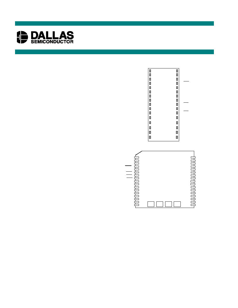
PIN ASSIGNMENT
DS1647/DS1647P
Nonvolatile Timekeeping RAM
www.maxim-ic.com
1
NC
2
3
A15
A16
PFO
V
CC
WE
OE
CE
DQ7
DQ6
DQ5
DQ4
DQ3
DQ2
DQ1
DQ0
GND
4
5
6
7
8
9
10
11
12
13
14
15
16
17
A17
A14
33
32
31
30
29
28
27
26
25
24
23
22
21
20
19
18
A13
A12
A11
A10
A9
A8
A7
A6
A5
A4
A3
A2
A1
A0
34
A18
X1 GND V
BAT
X2
34-Pin PowerCap Module Board
(Uses DS9034PCX PowerCap)
13
1
2
3
4
5
6
7
8
9
10
11
12
14
31
32-Pin Encapsulated Package
A14
A7
A5
A4
A3
A2
A1
A0
DQ1
DQ0
V
CC
A15
A17
WE
A13
A8
A9
A11
OE
A10
CE
DQ7
DQ5
DQ6
32
30
29
28
27
26
25
24
23
22
21
19
20
A16
A12
A6
A18
DQ2
GND
15
16
18
17
DQ4
DQ3

DS1647/DS1647P
2 of 11
PIN DESCRIPTION
A0-A18
- Address Input
CE
- Chip Enable
OE
- Output Enable
WE
- Write Enable
V
CC
-
+5V
GND -
Ground
DQ0-DQ7 -
Data
Input/Output
NC
- No Connection
PFO
- Power-fail Output
(DS1647P only)
X1, X2
- Crystal Connection
V
BAT
- Battery Connection
DESCRIPTION
The DS1647 is a 512k x 8 nonvolatile static RAM with a full-function real-time clock, which are both
accessible in a byte-wide format. The nonvolatile timekeeping RAM is functionally equivalent to any
JEDEC standard 512k x 8 SRAM. The device can also be easily substituted for ROM, EPROM and
EEPROM, providing read/write nonvolatility and the addition of the real-time clock function. The real-
time clock information resides in the eight uppermost RAM locations. The RTC registers contain year,
month, date, day, hours, minutes, and seconds data in 24-hour BCD format. Corrections for the day of the
month and leap year are made automatically. The RTC clock registers are double-buffered to avoid access
of incorrect data that can occur during clock update cycles. The double-buffered system also prevents
time loss as the timekeeping countdown continues unabated by access to time register data. The DS1647
also contains its own power-fail circuitry, which deselects the device when the V
CC
supply is in an out-of-
tolerance condition. This feature prevents loss of data from unpredictable system operation brought on by
low V
CC
as errant access and update cycles are avoided.
PACKAGES
The DS1647 is available in two packages: 32-pin DIP and 34-pin PowerCap module. The 32-pin DIP
style module integrates the crystal, lithium energy source, and silicon all in one package. The 34-pin
PowerCap Module Board is designed with contacts for connection to a separate PowerCap (DS9034PCX)
that contains the crystal and battery. This design allows the PowerCap to be mounted on top of the
DS1647P after the completion of the surface mount process. Mounting the PowerCap after the surface
mount process prevents damage to the crystal and battery due to the high temperatures required for solder
reflow. The PowerCap is keyed to prevent reverse insertion. The PowerCap Module Board and PowerCap
are ordered separately and shipped in separate containers. The part number for the PowerCap is
DS9034PCX.
CLOCK OPERATIONS - READING THE CLOCK
While the double-buffered register structure reduces the chance of reading incorrect data, internal updates
to the DS1647 clock registers should be halted before clock data is read to prevent reading of data in
transition. However, halting the internal clock register updating process does not affect clock accuracy.
Updating is halted when a 1 is written into the read bit, the 7th most significant bit in the control register.
As long as 1 remains in that position, updating is halted. After a halt is issued, the registers reflect the
count, that is day, date, and time that was present at the moment the halt command was issued. However,
the internal clock registers of the double-buffered system continue to update so that clock accuracy is not
affected by the access of data. All of the DS1647 registers are updated simultaneously after the clock
status is reset. Updating is within a second after the read bit is written to 0.
DS1647/DS1647P
3 of 11
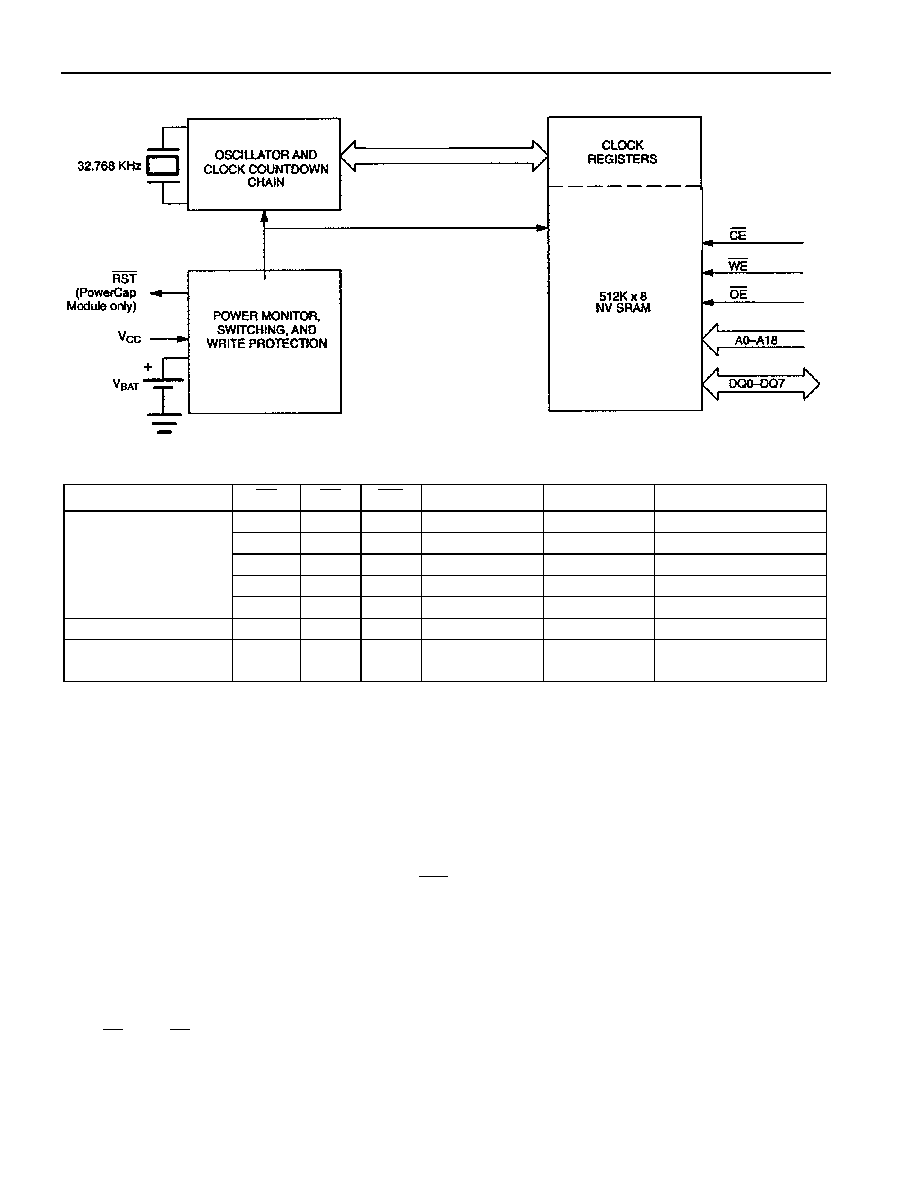
BLOCK DIAGRAM DS1647 Figure 1
TRUTH TABLE DS1647 Table 1
V
CC
CE
OE
WE
MODE
DQ
POWER
V
IH
X
X
DESELECT
HIGH-Z
STANDBY
X
X
X
DESELECT
HIGH-Z
STANDBY
V
IL
X
V
IL
WRITE
DATA IN
ACTIVE
V
IL
V
IL
V
IH
READ
DATA OUT
ACTIVE
5V
± 10%
V
IL
V
IH
V
IH
READ
HIGH-Z
ACTIVE
<4.5V >V
BAT
X
X
X
DESELECT
HIGH-Z
CMOS STANDBY
<V
BAT
X
X
X
DESELECT
HIGH-Z
DATA RETENTION
MODE
SETTING THE CLOCK
The MSB Bit, B7, of the control register is the write bit. Setting the write bit to a 1, like the read bit halts
updates to the DS1647 registers. The user can then load them with the correct day, date and time data in
24-hour BCD format. Resetting the write bit to a 0 then transfers those values to the actual clock counters
and allows normal operation to resume.
STOPPING AND STARTING THE CLOCK OSCILLATOR
The clock oscillator may be stopped at any time. To increase the shelf life, the oscillator can be turned off
to minimize current drain from the battery. The
OSC
bit is the MSB for the second's registers. Setting it
to a 1 stops the oscillator.
FREQUENCY TEST BIT
Bit 6 of the day byte is the frequency test bit. When the frequency test bit is set to logic 1 and the
oscillator is running, the LSB of the second's register will toggle at 512 Hz. When the seconds register is
being read, the DQ0 line will toggle at the 512 Hz frequency as long as conditions for access remain valid
(i.e.,
CE
low,
OE
low, and address for seconds register remain valid and stable).
DS1647/DS1647P
4 of 11
CLOCK ACCURACY (DIP MODULE)
The DS1647 is guaranteed to keep time accuracy to within
±1 minute per month at 25°C. The RTC is
calibrated at the factory by Dallas Semiconductor using nonvolatile tuning elements, and does not require
additional calibration. For this reason, methods of field clock calibration are not available and not
necessary. Clock accuracy is also effected by the electrical environment and caution should be taken to
place the RTC in the lowest level EMI section of the PCB layout. For additional information please see
application note 58.
CLOCK ACCURACY (POWERCAP MODULE)
The DS1647 and DS9034PCX are each individually tested for accuracy. Once mounted together, the
module will typically keep time accuracy to within
±1.53 minutes per month (35 ppm) at 25°C. Clock
accuracy is also effected by the electrical environment and caution should be taken to place the RTC in
the lowest level EMI section of the PCB layout. For additional information please see application
note 58.
1646 REGISTER MAP - BANK1 Table 2
DATA
ADDRESS
B
7
B
6
B
5
B
4
B
3
B
2
B
1
B
0
FUNCTION
7FFFF
-
-
-
-
-
-
-
-
YEAR
00-99
7FFFE
X
X
X
-
-
-
-
-
MONTH
01-12
7FFFD
X
X
-
-
-
-
-
-
DATE
01-31
7FFFC
X
FT
X
X
X
-
-
-
DAY
01-07
7FFFB
X
X
-
-
-
-
-
-
HOUR
00-23
7FFFA
X
-
-
-
-
-
-
-
MINUTES
00-59
7FFF9
OSC
-
-
-
-
-
-
-
SECONDS
00-59
7FFF8
W
R
X
X
X
X
X
X
CONTROL
A
OSC
= STOP BIT
R = READ BIT
FT = FREQUENCY TEST
W = WRITE BIT
X = UNUSED
NOTE:
All indicated "X" bits are not dedicated to any particular function and can be used as normal RAM bits.

DS1647/DS1647P
5 of 11
RETRIEVING DATA FROM RAM OR CLOCK
The DS1647 is in the read mode whenever
WE
(write enable) is high;
CE
(chip enable) is low. The
device architecture allows ripple-through access to any of the address locations in the NV SRAM. Valid
data will be available at the DQ pins within t
AA
after the last address input is stable, providing that the
CE
and
OE
access times and states are satisfied. If
CE
or
OE
access times are not met, valid data will be
available at the latter of chip-enable access (t
CEA
) or at output enable access time (t
OEA
). The state of the
data input/output pins (DQ) is controlled by
CE
and
OE
. If the outputs are activated before t
AA
, the data
lines are driven to an intermediate state until t
AA
. If the address inputs are changed while
CE
and
OE
remain valid, output data will remain valid for output data hold time (t
OH
) but will then go indeterminate
until the next address access.
WRITING DATA TO RAM OR CLOCK
The DS1647 is in the write mode whenever
WE
and
CE
are in their active state. The start of a write is
referenced to the latter occurring high to low transition of
WE
and
CE
. The addresses must be held valid
throughout the cycle.
CE
or
WE
must return inactive for a minimum of t
WR
prior to the initiation of
another read or write cycle. Data in must be valid t
DS
prior to the end of write and remain valid for t
DH
afterward. In a typical application, the
OE
signal will be high during a write cycle. However,
OE
can be
active provided that care is taken with the data bus to avoid bus contention. If
OE
is low prior to
WE
transitioning low the data bus can become active with read data defined by the address inputs. A low
transition on
WE
will then disable the outputs t
WEZ
after
WE
goes active.
DATA RETENTION MODE
When V
CC
is within nominal limits (V
CC
> 4.5 volts) the DS1647 can be accessed as described above with
read or write cycles. However, when V
CC
is below the power-fail point V
PF
(point at which write
protection occurs) the internal clock registers and RAM are blocked from access. This is accomplished
internally by inhibiting access via the
CE
signal. At this time the power-fail output signal (
PFO
) will be
driven active low and will remain active until V
CC
returns to nominal levels. When V
CC
falls below the
level of the internal battery supply, power input is switched from the V
CC
pin to the internal battery and
clock activity, RAM, and clock data are maintained from the battery until V
CC
is returned to nominal
level.