1 of 17
REV: 082203
Note: Some revisions of this device may incorporate deviations from published specifications known as errata. Multiple revisions of any device
may be simultaneously available through various sales channels. For information about device errata, click here:
www.maxim-ic.com/errata
.
FEATURES
§ Real-time clock (RTC) keeps track of hundredths
of seconds, seconds, minutes, hours, days, date,
months, and years with automatic leap-year
compensation valid up to the year 2100
§ 2M x 8 NV SRAM
§ Watch function is transparent to RAM operation
§ Automatic data protection during power loss
§ Unlimited write-cycle endurance
§ Surface-mountable BGA module construction
§ Over 10 years of data retention in the absence of
power
§ Battery monitor checks remaining capacity daily
§ +3.3V or +5V operation
APPLICATIONS
Telecom Switches
Routers
RAID Systems
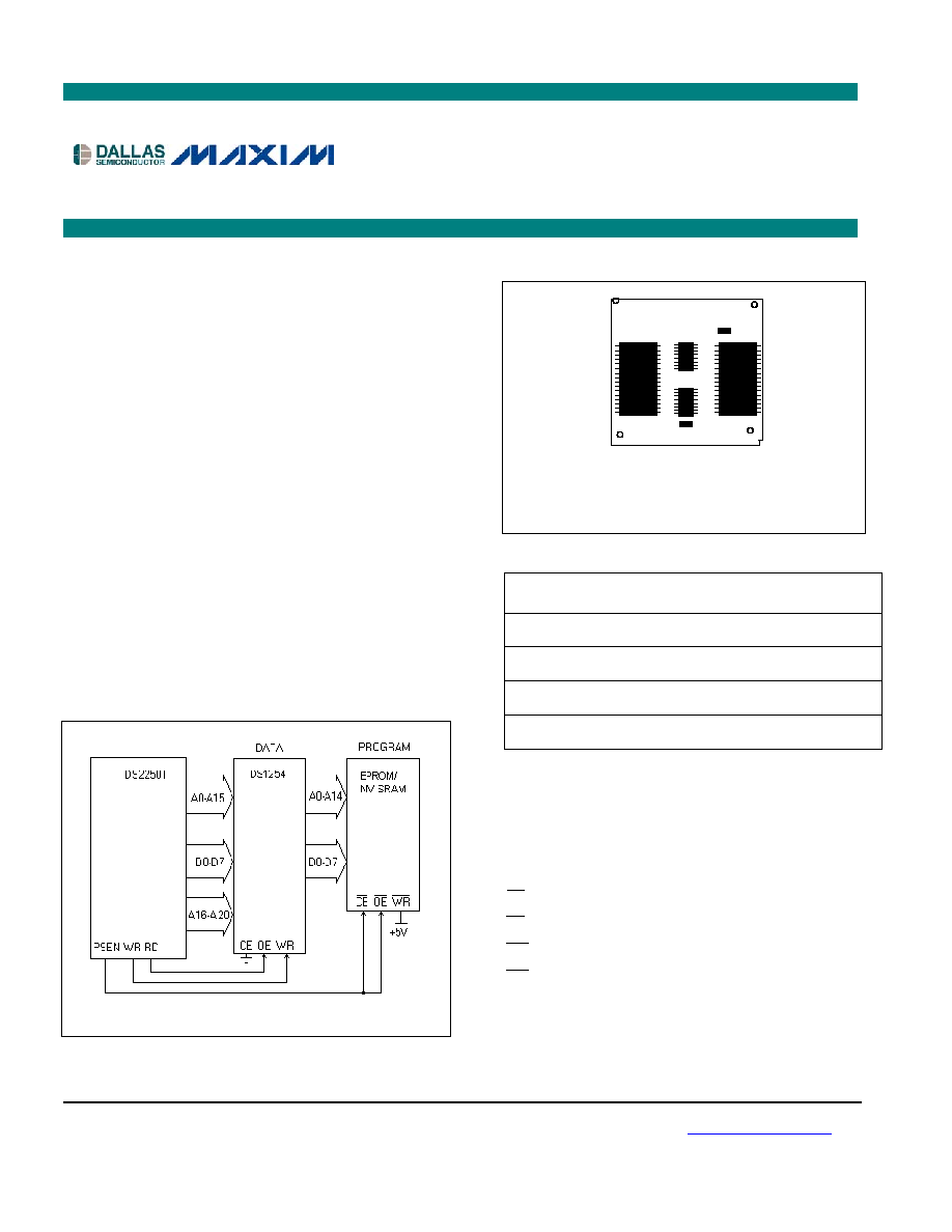
TYPICAL OPERATING CIRCUIT
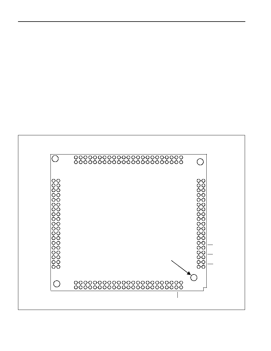
PACKAGE OUTLINE
ORDERING INFORMATION
PART
PIN-
PACKAGE
TEMP
RANGE
TOP
MARK
DS1254WB-
150
BGA, 3.3V
0°C to +70°C
DS1254W-
150
DS1254YB-
100
BGA, 5V
0°C to +70°C
DS1254Y-
100
DS1254WB2-
150
BGA, 3.3V
0°C to +70°C
DS1254W2-
150
DS1254YB2-
100
BGA, 5V
0°C to +70°C
DS1254Y2-
100
PIN DESCRIPTION
V
CC
- Supply Voltage
A0A20 -
Address
Inputs
DQ0DQ7 -
Data
I/O
CE
-
Chip-Enable
Input
OE
-
Output-Enable
Input
WE
-
Write-Enable
Input
BW
- Battery Warning Output
(Open Drain)
GND
-
Ground
DS1254
2M x 8 NV SRAM with Phantom Clock
www.maxim-ic.com
Side -A- Shown
(For Reference Only, Not to Scale)
Component placement may vary.
DS1254
2 of 17
DESCRIPTION
The DS1254 is a fully nonvolatile static RAM (NV SRAM) (organized as 2M words by 8 bits) with built-
in real-time clock. It has a self-contained lithium energy source and control circuitry that constantly
monitors V
CC
for an out-of-tolerance condition. When such a condition occurs, the DS1254 makes use of
an attached DS3800 battery cap to maintain clock information and preserve stored data while protecting
that data by disallowing all memory accesses. Additionally, the DS1254 has dedicated circuitry for
monitoring the status of an attached DS3800 battery cap.
The phantom clock provides timekeeping information including hundredths of seconds, seconds, minutes,
hours, day, date, month, and year information. The date at the end of the month is automatically adjusted
for months with fewer than 31 days, including correction for leap years. The phantom clock operates in
either 24-hour or 12-hour format with an AM/PM indicator.
Because the DS1254 has a total of 168 balls and only 35 active signals, balls are wired together into
groups, thus providing redundant connections for every signal.
Figure 1. Pin Assignment
V
CC
A7
A6
A5
GND
A4
A3
A2
A1
1
2
3
4
5
6
7
8
9
29
28
27
26
25
24
23
22
21
10
11
12
13
14
15
16
17
18
19
20
41
40
39
38
37
36
35
34
33
32
31
30
V
CC
A17
A18
A19
GND
A20
CE
OE
WE
A0
DQ0
DQ1
DQ2
DQ3
GND
DQ4
DQ5
DQ6
DQ7
B
W
V
CC
A
8
A
9
A
10
A
11
GND
A
12
A
13
A
14
A
15
A
16
V
CC
RECEPTACLES FOR
DS3800 BATTERY CAP
PINS
GND
V
BAT
Dallas Semiconductor
DS1254

DS1254
3 of 17
RAM READ MODE
The DS1254 executes a read cycle whenever
WE
is inactive (high) and
CE
is active (low). The unique
address specified by the 21 address inputs (A0A20) defines which of the 2MB of data is to be accessed.
Valid data will be available to the eight data-output drivers within t
ACC
(access time) after the last address
input is stable, providing that
CE
and
OE
access times and states are also satisfied. If
OE
and
CE
access
times are not satisfied, then data access must be measured from the later occurring signal (
CE
or
OE
) and
the limiting parameter is either t
CO
for
CE
or t
OE
for
OE
rather than address access.
RAM WRITE MODE
The DS1254 is in the write mode whenever
WE
and
CE
are in their active (low) state after address inputs
are stable. The later occurring falling edge of
CE
or
WE
will determine the start of the write cycle. The
write cycle is terminated by the earlier rising edge of
CE
or
WE
. All address inputs must be kept valid
throughout the write cycle.
WE
must return to the high state for a minimum recovery time (t
WR
) before
another cycle can be initiated. The
OE
control signal should be kept inactive (high) during write cycles to
avoid bus contention. However, if the output bus has been enabled (
CE
and
OE
active), then
WE
will
disable the outputs in t
ODW
from its falling edge.
DATA RETENTION MODE
The device is fully accessible and data can be written and read only when V
CC
is greater than V
PF
.
However, when V
CC
falls below the power-fail point, V
PF
(point at which write protection occurs), the
internal clock registers and SRAM are blocked from any access. When V
CC
falls below V
BAT
, device
power is switched from the V
CC
to V
BAT
. RTC operation and SRAM data are maintained from the battery
until V
CC
is returned to nominal levels. All signals must be powered down when V
CC
is powered down.
PHANTOM CLOCK OPERATION
Communication with the phantom clock is established by pattern recognition on a serial bit stream of
64 bits that must be matched by executing 64 consecutive write cycles containing the proper data on
DQ0. All accesses that occur prior to recognition of the 64-bit pattern are directed to memory.
After recognition is established, the next 64 read or write cycles either extract or update data in the
phantom clock, and memory access is inhibited.
Data transfer to and from the timekeeping function is accomplished with a serial bit stream under control
of chip enable (
CE
), output enable (
OE
), and write enable (
WE
). Initially, a read cycle to any memory
location using the
CE
and
OE
control of the phantom clock starts the pattern-recognition sequence by
moving a pointer to the first bit of the 64-bit comparison register. Next, 64 consecutive write cycles are
executed using the
CE
and
WE
signals of the device. These 64 write cycles are used only to gain access to
the phantom clock. Therefore, any address within the first 512kB of memory, (00h to 7FFFFh) is
acceptable. However, the write cycles generated to gain access to the phantom clock are also writing data
to a location in the memory. The preferred way to manage this requirement is to set aside just one address
location in memory as a phantom clock scratch pad. When the first write cycle is executed, it is compared
to bit 0 of the 64-bit comparison register. If a match is found, the pointer increments to the next location
of the comparison register and awaits the next write cycle. If a match is not found, the pointer does not
DS1254
4 of 17
advance and all subsequent write cycles are ignored. If a read cycle occurs at any time during pattern
recognition, the present sequence is aborted and the comparison register pointer is reset. Pattern
recognition continues for a total of 64 write cycles as described above until all the bits in the comparison
register have been matched (this bit pattern is shown in Figure 2). With a correct match for 64-bits, the
phantom clock is enabled and data transfer to or from the timekeeping registers can proceed. The next 64
cycles will cause the phantom clock to either receive or transmit data on DQ0, depending on the level of
the
OE
pin or the
WE
pin. Cycles to other locations outside the memory block can be interleaved with
CE
cycles without interrupting the pattern-recognition sequence or data-transfer sequence to the phantom
clock.
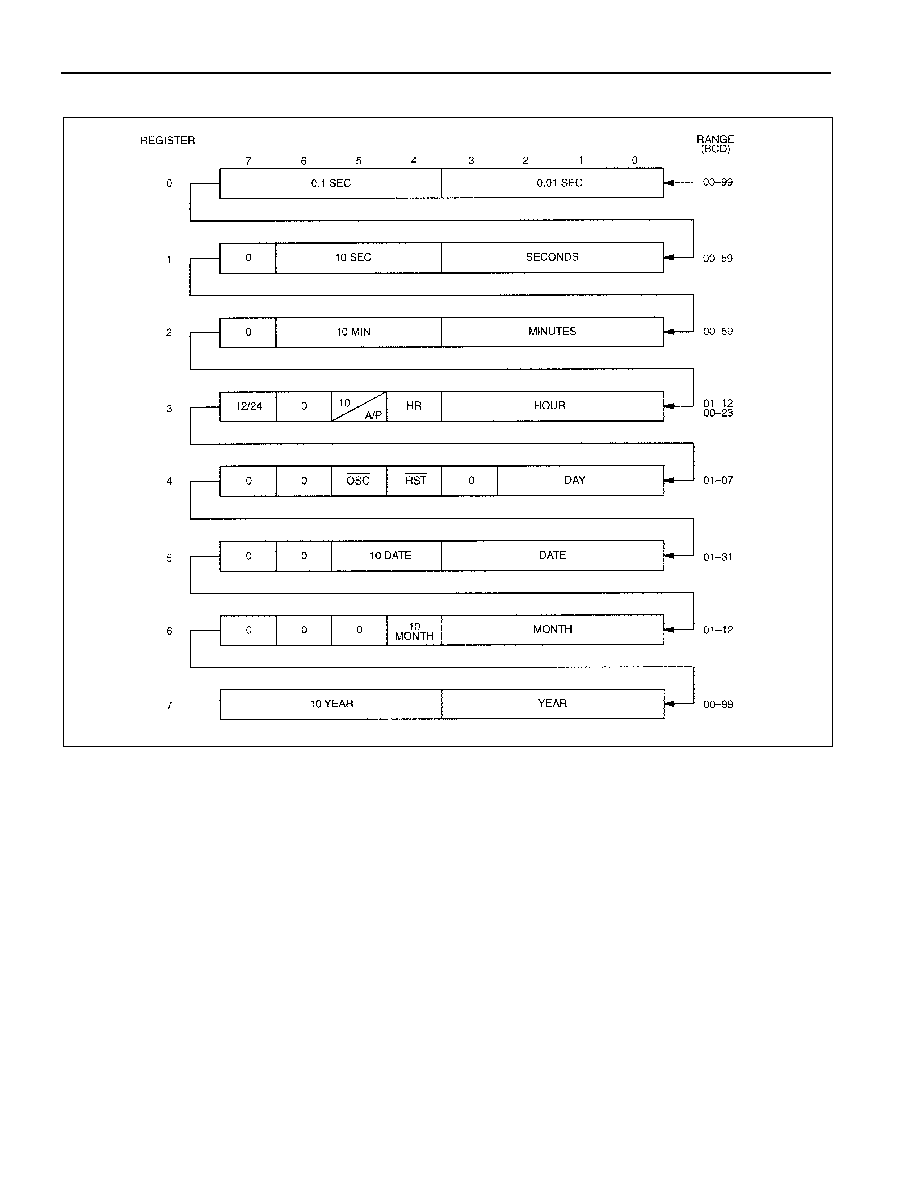
PHANTOM CLOCK REGISTER INFORMATION
The phantom clock information is contained in eight registers of 8 bits, each of which is sequentially
accessed one bit at a time after the 64-bit pattern-recognition sequence has been completed. When
updating the phantom clock registers, each register must be handled in groups of 8 bits. Writing and
reading individual bits within a register could produce erroneous results. These read/write registers are
defined in Figure 3.
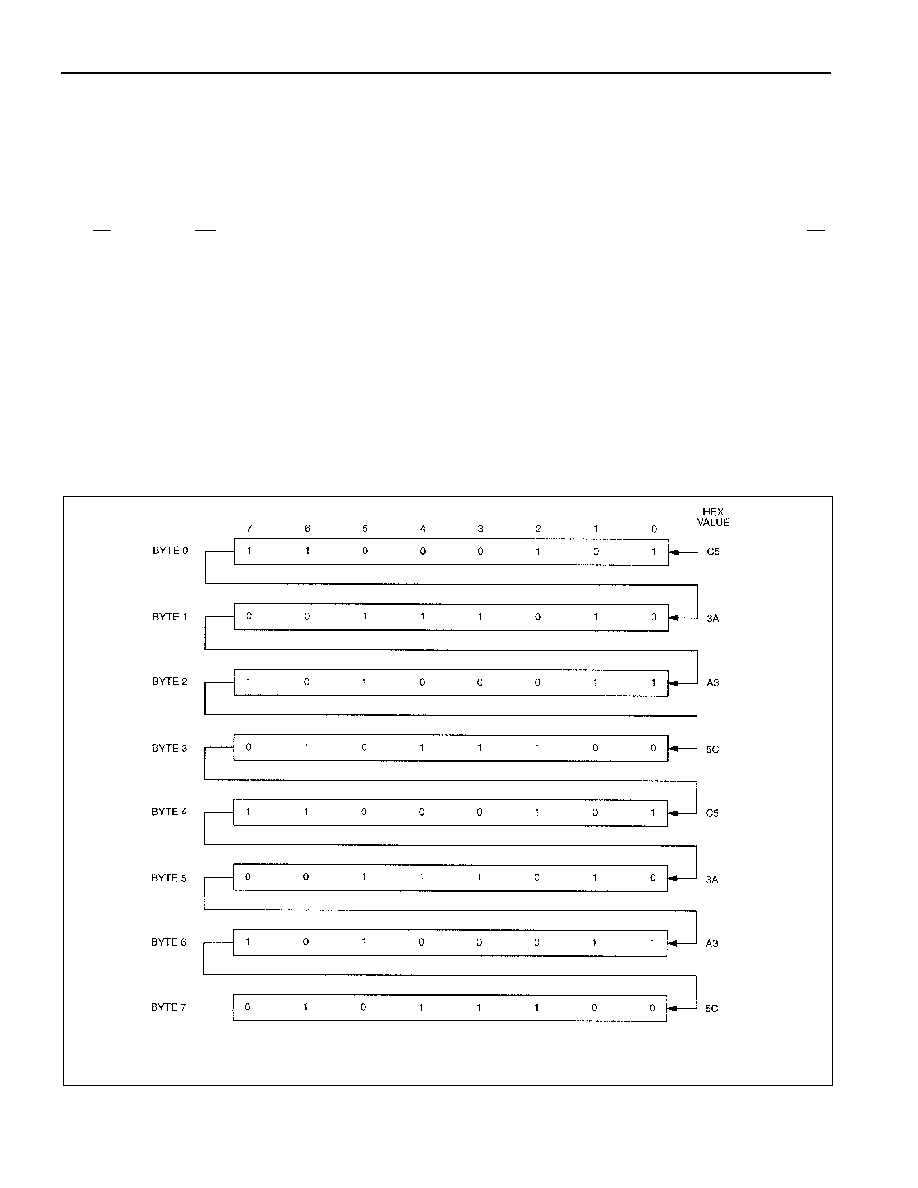
Figure 2. Phantom Clock Protocol Definition
NOTE: THE PATTERN RECOGNITION IN HEX IS C5, 3A, A3, 5C, C5, 3A, A3, 5C. THE ODDS OF THIS PATTERN BEING
ACCIDENTALLY DUPLICATED AND CAUSING INADVERTENT ENTRY TO THE PHANTOM CLOCK IS LESS THAN 1 IN 10
19
. THIS
PATTERN IS SENT TO THE PHANTOM CLOCK LSB TO MSB.