1 of 6
061500
FEATURES
All-silicon timing circuit
Three independent buffered delays
Stable and precise over temperature and
voltage
Leading and trailing edge precision preserves
the input symmetry
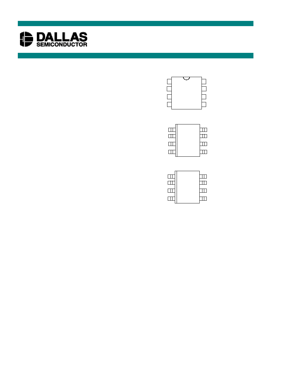
Standard 8-pin DIP and 8-pin SOIC
(150 mil)
Vapor phasing, IR and wave solderable
Available in Tape and Reel
Commercial and industrial temperature ranges
available; see order info table
5V operation (for 3V operation, see part
number DS1135L)
Recommended replacement for DS1013 and
DS1035
PIN ASSIGNMENT
PIN DESCRIPTION
IN1-IN3
-
Input
Signals
OUT1-OUT3
- Output Signals
V
CC
- +5V Supply
GND -
Ground
DESCRIPTION
The DS1135 series is a low-power, +5-volt high-speed version of the popular DS1013 and DS1035.
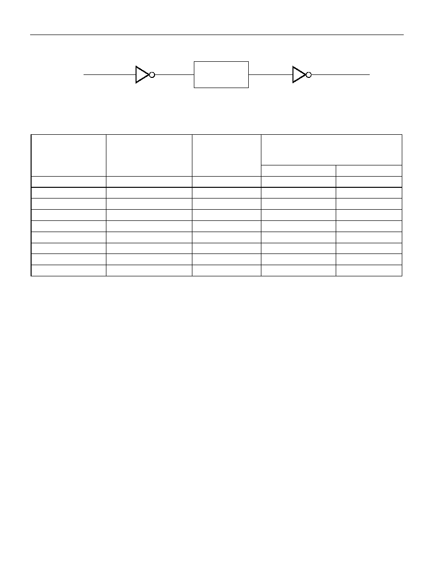
The DS1135 series of delay lines have three independent logic buffered delays in a single package. The
device is Dallas Semiconductor's fastest 3-in-1 delay line. It is available in a standard 8-pin DIP and
150 mil 8-pin Mini-SOIC, as well as an 8-pin, 118 mil uSOP.
The device features precise leading and trailing edge accuracy. It has the inherent reliability of an all-
silicon delay line solution. Each output is capable of driving up to 10 LS loads.
Standard delay values are indicated in Table 1. Customers may contact Dallas Semiconductor at
(972) 371-4348 for further information on custom delay values.
DS1135
3-in-1 High-Speed Silicon Delay Line
www.dalsemi.com
DS1135M 8-Pin DIP
IN2
GND
V
CC
OUT1
OUT2
OUT3
7
1
2
3
4
8
6
5
IN3
IN1
DS1135Z 8-Pin SOIC (150 mil)
1
2
3
4
7
8
6
5
IN2
GND
IN3
IN1
V
CC
OUT1
OUT2
OUT3
PRELIMINARY
DS1135U 8-Pin 118-mil uSOP
1
2
3
4
7
8
6
5
IN2
GND
IN3
IN1
V
CC
OUT1
OUT2
OUT3
DS1135
2 of 6
LOGIC DIAGRAM Figure 1
PART NUMBER DELAY TABLE (t
PLH
, t
PHL
) Table 1
TOLERANCE OVER
TEMP AND VOLTAGE
(Note 2)
PART NUMBER
DELAY PER
OUTPUT
(ns)
INITIAL
TOLERANCE
(Note 1)
0�C to +70�C
-40�C to +85�C
DS1135-5
5/5/5
�
1.0 ns
�
1.0 ns
�
1.5 ns
DS1135-6
6/6/6
�
1.0 ns
�
1.0 ns
�
1.5 ns
DS1135-8
8/8/8
�
1.0 ns
�
1.0 ns
�
1.5 ns
DS1135-10
10/10/10
�
1.0 ns
�
1.0 ns
�
1.5 ns
DS1135-12
12/12/12
�
1.0 ns
�
1.0 ns
�
1.5 ns
DS1135-15
15/15/15
�
1.0 ns
�
1.5 ns
�
2 ns
DS1135-20
20/20/20
�
1.0 ns
�
1.5 ns
�
2 ns
DS1135-25
25/25/25
�
1.5 ns
�
1.5 ns
�
2 ns
DS1135-30
30/30/30
�
1.5 ns
�
1.5 ns
�
2 ns
NOTES:
1.
Nominal conditions are +25�C and V
CC
=+5.0 volts.
2.
Voltage range of 4.75 volts to 5.25 volts.
3.
Delay accuracies are for both leading and trailing edges.
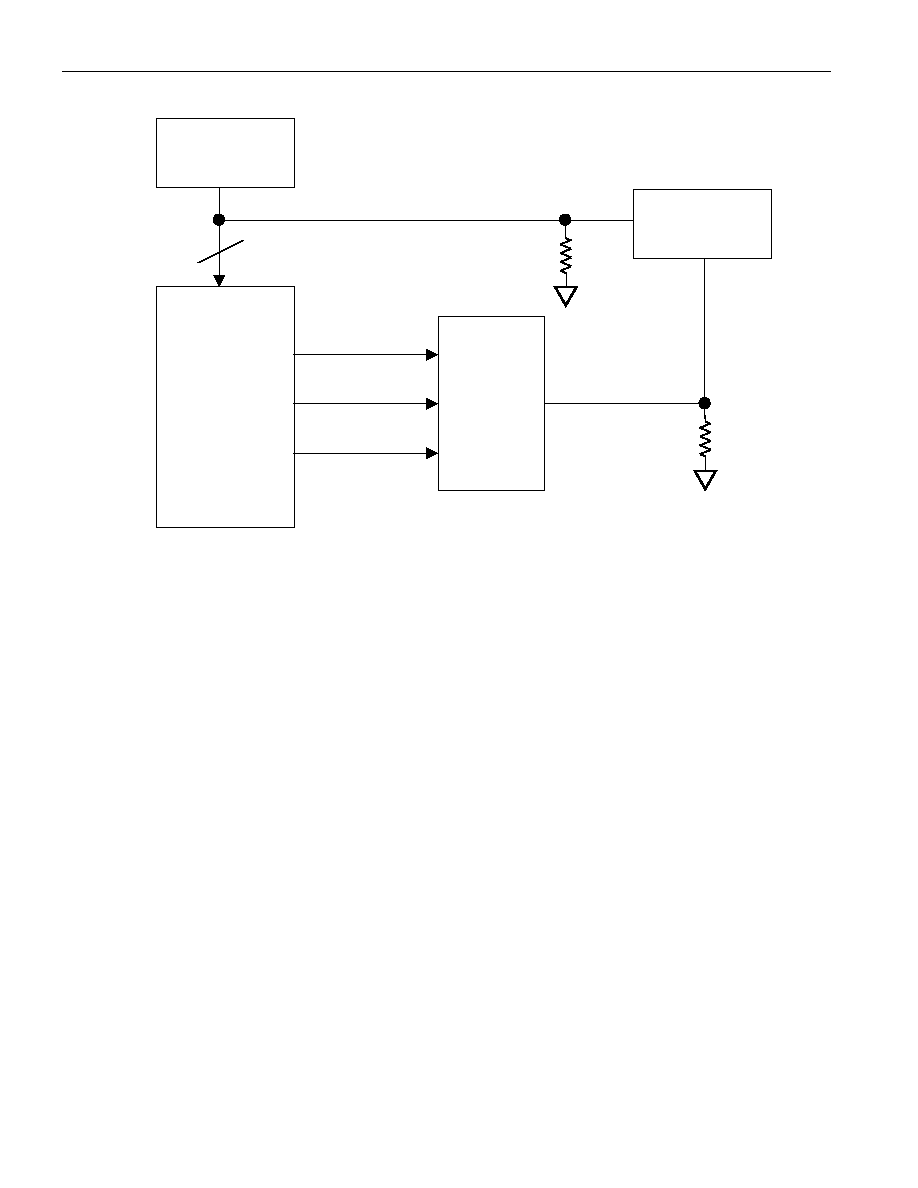
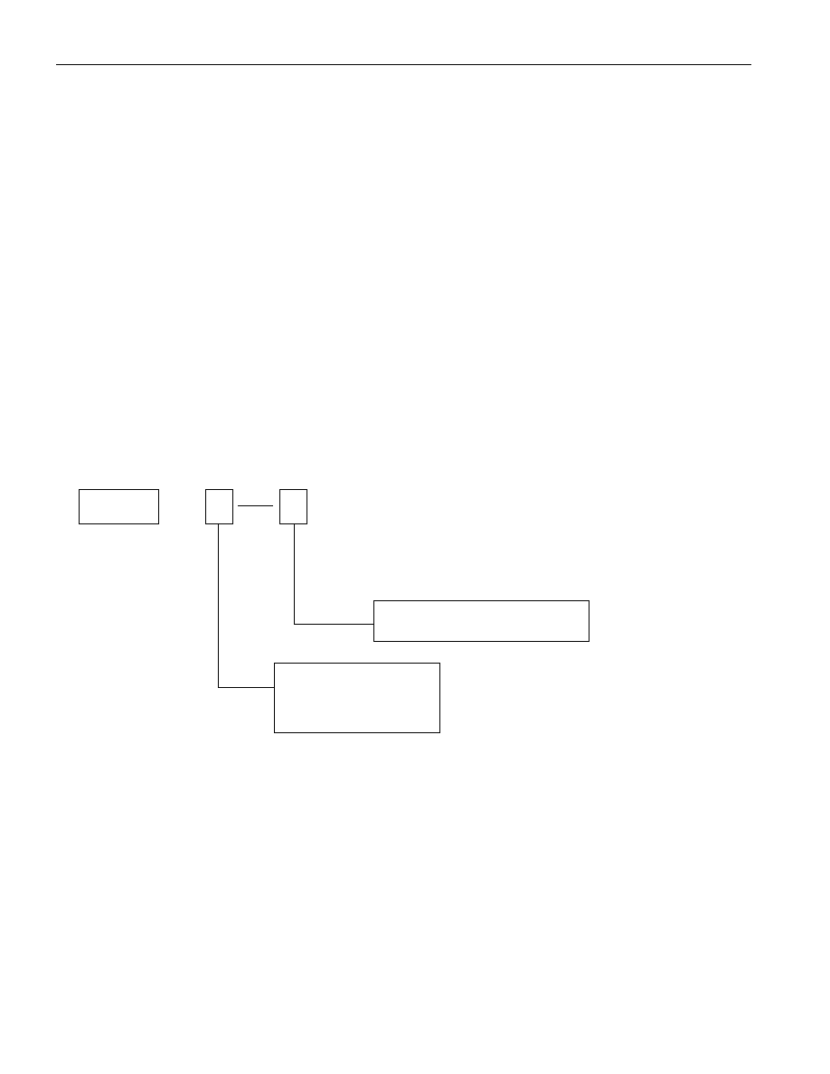
TEST SETUP DESCRIPTION
Figure 2 illustrates the hardware configuration used for measuring the timing parameters of the DS1135.
The input waveform is produced by a precision pulse generator under software control. Time delays are
measured by a time interval counter (20 ps resolution ) connected to the output. The DS1135 output taps
are selected and connected to the interval counter by a VHF switch control unit. All measurements are
fully automated with each instrument controlled by the computer over an IEEE 488 bus.
TIME DELAY
OUT
IN
ONE OF THREE
DS1135
3 of 6
DS1135 TEST CIRCUIT Figure 2
PULSE
GENERATOR
UNIT UNDER
TEST
TAPS 1-3
START
50
STOP
50
OUT
3
IN
VHF
SWITCH
CONTROL
UNIT
TIME INTERVAL
COUNTER
DS1135
4 of 6
ABSOLUTE MAXIMUM RATINGS*
Voltage on Any Pin Relative to Ground
-1.0V to +7.0V
Operating Temperature
-40
�
C to +85
�
C
Storage Temperature
-55
�
C to +125
�
C
Soldering Temperature
See J-STD-020A specification
Short Circuit Output Current
50 mA for 1 second
* This is a stress rating only and functional operation of the device at these or any other conditions above
those indicated in the operation sections of this specification is not implied. Exposure to absolute
maximum rating conditions for extended periods of time may affect reliability.
DC ELECTRICAL CHARACTERISTICS
(-40
�
C to +85
�
C;V
CC
=+5V
�
5%)
PARAMETER
SYMBOL
TEST
CONDITION
MIN TYP
MAX
UNITS
NOTES
Supply Voltage
V
CC
4.75
5.00
5.25
V
1
Active Current
I
CC
V
CC
=5.25V
Period=1
�
s
35
mA
High Level Input Voltage
V
IH
2.2
V
CC
+0.5
V
1
Low Level Input Voltage
V
IL
-0.5
0.8
V
1
Input Leakage
I
L
0VV
I
V
CC
-1.0
+1.0
�
A
High Level Output
Current
I
CC
V
CC
=4.75V
V
OH
=4V
-1.0
mA
1
Low Level Output Current
I
CC
V
CC
=4.75V
V
OL
=0.5V
12
mA
1
AC ELECTRICAL CHARACTERISTICS
(-40
�
C to +85
�
C;V
CC
=+5V
�
5%)
PARAMETER
SYMBOL
MIN
TYP
MAX
UNITS
NOTES
Period
t
PERIOD
2 (t
WI
)
ns
2
Input Pulse Width
t
WI
100% of
Tap Delay
ns
2
Input-to-Output Delay
t
PLH
,
t
PHL
See Table 1
ns
Output Rise or Fall Time
t
OF
, t
OR
2.0
2.5
ns
Power-up Time
t
PU
100
ms
3
CAPACITANCE
(T
A
=25
�
C)
PARAMETER
SYMBOL
MIN
TYP
MAX
UNITS
NOTES
Input Capacitance
C
IN
10
pF
DS1135
5 of 6
TEST CONDITIONS
Ambient Temperature: 25
�
C
�
=3
�
C
Supply Voltage (V
CC
): 5.0V
�
=0.1V
Input Pulse:
High: 3.0V
�
=0.1V
Low: 0.0V
�
=0.1V
Source Impedance: 50
=Max.
Rise and Fall Time: 3.0 ns Max. - Measured between 0.6V and 2.4V.
Pulse Width: 500 ns
Pulse Period: 1
�
s
Output Load Capacitance: 15 pF
Output: Each output is loaded with the equivalent of one 74F04 input gate.
Data is measured at the 1.5V level on the rising and falling edges.
NOTE:
The above conditions are for test only and do not restrict the devices under other data sheet conditions.
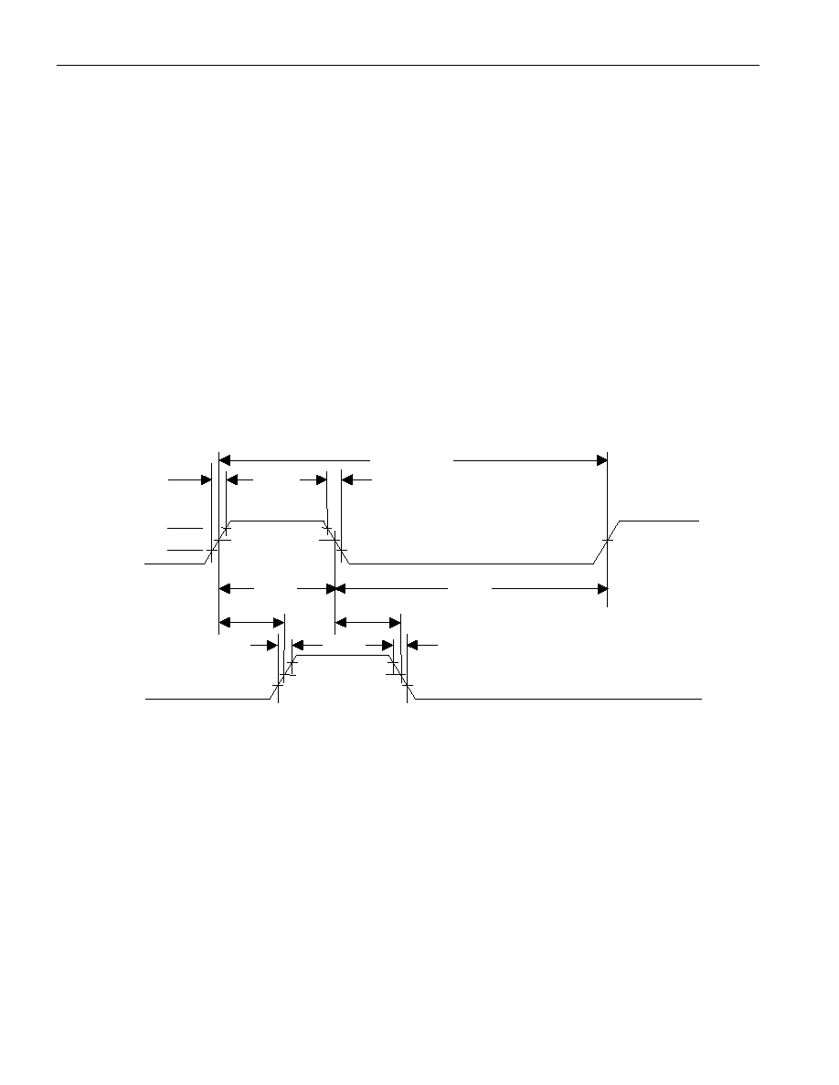
TIMING DIAGRAM
NOTES:
1.
All voltages are referenced to ground.
2.
Pulse width and duty cycle specifications may be exceeded, however, accuracy will be application
sensitive with respect to decoupling, layout, etc.
3.
Power-up time is the time from the application of power to the time stable delays are being produced
at the output.
t
FALL
80%
t
RISE
20%
IN
OUT
1.5V
1.5V
t
WI
t
WI
PERIOD
1.5V
1.5V
1.5V
t
PLH
t
PHL
t
OF
t
OR
DS1135
6 of 6
TERMINOLOGY
Period: The time elapsed between the leading edge of the first pulse and the leading edge of the
following pulse.
t
WI
(Pulse Width): The elapsed time on the pulse between the 1.5-volt point on the leading edge and the
1.5-volt point on the trailing edge or the 1.5-volt point on the trailing edge and the 1.5-volt point on the
leading edge.
t
RISE
(Input Rise Time): The elapsed time between the 20% and the 80% point on the leading edge of the
input pulse.
t
FALL
(Input Fall Time): The elapsed time between the 80% and the 20% point on the trailing edge on the
input pulse.
t
PLH
(Time Delay, Rising): The elapsed time between the 1.5-volt point on the leading edge of the input
pulse and the 1.5-volt point on the leading edge of the output pulse.
t
PHL
(Time Delay, Falling): The elapsed time between the 1.5-volt point on the falling edge of the input
pulse and the 1.5-volt point on the falling edge of the output pulse.
ORDERING INFORMATION
DS1135
TIME DELAY (ns): 5, 6, 8, 10, 12, 15, 20,
25, 30
PACKAGE TYPE:
M = DIP
Z = SOIC (150 Mil)
U = uSOP (118 Mil)