
1 of 16
022300
FEATURES
Step sizes of 0.25 ns, 0.5 ns, 1 ns, 2 ns, 5 ns
On-chip reference delay
Configurable as delay line, pulse width
modulator, or free-running oscillator
Can delay clocks by a full period or more
Guaranteed monotonicity
Parallel or serial programming
Single 5V supply
16-pin DIP or SOIC package
PIN ASSIGNMENT
PIN DESCRIPTION
IN -
Input
P0/Q
- Parallel Input P0 (parallel mode)
- Serial Data Output (serial mode)
P1/CLK
- Parallel Input P1 (parallel mode)
- Serial Input Clock (serial mode)
P2/D
- Parallel Input P2 (parallel mode)
- Serial Data Input (serial mode)
P3 - P7
- Remaining Parallel Inputs
GND -
Ground
OUT/
OUT
-
Output
REF/PWM
- Reference or PWM Output
P
/S
- Parallel / Serial Programming
Select
MS
- Output Mode Select
LE
- Input Latch Enable
V
CC
- Supply Voltage
DESCRIPTION
The DS1023 is an 8-bit programmable delay line similar in function to the DS1020/DS1021.
Additional features have been added to extend the range of applications:
The internal delay line architecture has been revised to allow clock signals to be delayed by up to a full
period or more. Combined with an on-chip reference delay (to offset the inherent or "step zero" delay of
the device) clock phase can now be varied over the full 0-360 degree range.
DS1023
8-Bit Programmable Timing Element
www.dalsemi.com
IN
LE
Q/P0
CLK/P1
D/P2
P3
P4
GND
16
15
14
13
12
11
10
9
V
CC
OUT/OUT
REF/PWM
P/S
P7
P6
MS
P5
1
2
3
4
5
6
7
8
DS1023 300-mil DIP
DS1023S 300-mil SOIC

DS1023
2 of 16
On-chip gating is provided to allow the device to provide a pulse width modulated output, triggered by
the input with duration set by the programmed value.
Alternatively the output signal may be inverted on chip, allowing the device to perform as a free-running
oscillator if the output is (externally) connected to the input.
PROGRAMMING
The device programming is identical to the DS1020/DS1021. Note, however, that the serial clock and
data pins are shared with three of the parallel input pins.
The
P
/S pin controls the same function as "Mode Select" on the DS1020/DS1021 (but with reversed
polarity). A low logic level on this pin enables the parallel programming mode. LE must be at a high
logic level to alter the programmed value; when LE is taken low the data is latched internally and the
parallel data inputs may be altered without affecting the programmed value. This is useful for
multiplexed bus applications. For hard-wired applications LE should be tied to a high logic level.
When
P
/S is high serial programming is enabled. LE must be held high to enable loading or reading of
the internal register, during which time the delay is determined by the previously programmed value.
Data is clocked in MSB to LSB order on the rising edge of the CLK input. Data transfer ends and the
new value is activated when LE is taken low.
PARALLEL MODE (
P
/S = 0)
In the PARALLEL programming mode, the output of the DS1023 will reproduce the logic state of the
input after a delay determined by the state of the eight program input pins P0 - P7. The parallel inputs
can be programmed using DC levels or computer-generated data. For infrequent modification of the
delay value, jumpers may be used to connect the input pins to V
CC
or ground. For applications requiring
frequent timing adjustment, DIP switches may be used. The latch enable pin (LE) must be at a logic 1 in
hardwired implementations.
Maximum flexibility is obtained when the eight parallel programming bits are set using computer-
generated data. When the data setup (t
DSE
) and data hold (t
DHE
) requirements are observed, the enable pin
can be used to latch data supplied on an 8-bit bus. Latch enable must be held at a logic 1 if it is not used
to latch the data. After each change in delay value, a settling time (t
EDV
or t
PDV
) is required before input
logic levels are accurately delayed.
SERIAL MODE (
P
/S = 1)
In the SERIAL programming mode, the output of the DS1023 will reproduce the logic state of the input
after a delay time determined by an 8-bit value clocked into serial port D. While observing data setup
(t
DSC
) and data hold (t
DHC
) requirements, timing data is loaded in MSB-to-LSB order by the rising edge of
the serial clock (CLK). The latch enable pin (LE) must be at a logic 1 to load or read the internal 8-bit
input register, during which time the delay is determined by the last value activated. Data transfer ends
and the new delay value is activated when latch enable (LE) returns to a logic 0. After each change, a
settling time (t
EDV
) is required before the delay is accurate.
As timing values are shifted into the serial data input (D), the previous contents of the 8-bit input register
are shifted out of the serial output pin (Q) in MSB-to-LSB order. By connecting the serial output of one
DS1023 to the serial input of a second DS1023, multiple devices can be daisy-chained (cascaded) for
programming purposes (Figure 1). The total number of serial bits must be eight times the number of units
daisy-chained and each group of 8 bits must be sent in MSB-to-LSB order.

DS1023
3 of 16
Applications can read the setting of the DS1023 Delay Line by connecting the serial output pin (Q) to the
serial input (D) through a resistor with a value of 1 to 10 kohms (Figure 2). Since the read process is
destructive, the resistor restores the value read and provides isolation when writing to the device. The
resistor must connect the serial output (Q) of the last device to the serial input (D) of the first device of a
daisy chain (Figure 1). For serial readout with automatic restoration through a resistor, the device used to
write serial data must go to a high impedance state.
To initiate a serial read, latch enable (LE) is taken to a logic 1 while serial clock (CLK) is at a logic 0.
After a waiting time (t
EQV
), bit 7 (MSB) appears on the serial output (Q). On the first rising (0 --> 1)
transition of the serial clock (CLK), bit 7 (MSB) is rewritten and bit 6 appears on the output after a time
t
CQV
. To restore the input register to its original state, this clocking process must be repeated eight times.
In the case of a daisy chain, the process must be repeated eight times per package. If the value read is
restored before latch enable (LE) is returned to logic 0, no settling time (t
EDV
) is required and the
programmed delay remains unchanged.
Since the DS1023 is a CMOS design, unused input pins (P3 - P7) must be connected to well-defined logic
levels; they must not be allowed to float. Serial output Q/P0 should be allowed to float if unused.
CASCADING MULTIPLE DEVICES (DAISY CHAIN) Figure 1
SERIAL READOUT Figure 2
REFERENCE DELAY
In all delay lines there is an inherent, or "step zero", delay caused by the propagation delay through the
input and output buffers. In this device the step zero delay can be quite large compared to the delay step
size. To simplify system design a reference delay has been included on chip which may be used to
compensate for the step zero delay. In practice this means that if the device is supplied with a clock, for
example, the minimum programmed output delay is effectively zero with respect to the reference delay.

DS1023
4 of 16
For highest accuracy it is strongly recommended that the reference delay is used. Variations in input
voltage levels and transition times can significantly alter the measured delay from input to output. This
effect is totally removed if the reference delay output is used. Furthermore, adverse effects on step zero
delay caused by process temperature coefficients are also cancelled out.
INPUT PULSE DURATION
The internal architecture of the DS1023 allows the output delay time to be considerably longer than the
input pulse width (see ac specifications). This feature is useful in many applications, in particular clock
phase control where delays up to and beyond one full clock period can be achieved.
MODE SELECT
The DS1023 has four possible output functions but only two output pins. The functionality of the two
output pins is determined by the Mode Select (MS) pin.
MS = 0 Figure 3
Output Function
Name
Pin Number
Reference Output
REF
9
Delayed Output
OUT
15
OUT is a copy of the input waveform that is delayed by an amount set by the programmed values (Table
1). A programmed value of zero will still result in a non-zero delay as indicated in the Step Zero delay
specification. The signal on OUT is the same polarity as the input.
REF is a fixed reference delay. It also is a copy of the input waveform but the delay interval is fixed to a
value approximately equal to the Step Zero Value of the device (as shown in the Reference Delay
specification). In fact the device is trimmed to ensure that the Reference Delay is always slightly longer
than the Step Zero Value (by 1.5 ns typically).
DS1023
5 of 16
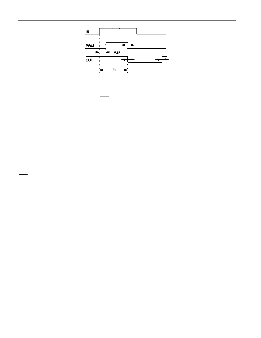
MS = 1 Figure 4
Output Function
Name
Pin Number
Pulse Width Modulated Output
PWM
9
Delayed and Inverted Output
OUT
15
PWM is an output triggered by the rising edge of the input waveform. After a time interval approximately
equal to the Step Zero delay of the device the PWM output will go high. The output will return to a low
level after a time interval determined by the programmed values (Table 1). Hence output pulse widths can
be obtained from (nearly) zero to the full delay range of the device. In practice the minimum output pulse
width is limited by the response time of the device to approximately 5ns. Programmed values less than
this will result in degradation of the output high level voltage until ultimately no discernible output pulse
is produced. The frequency/repetition rate of the output is determined by the input frequency. The input
pulse width can be shorter than the output pulse width, and is limited only by the minimum input pulse
width specification. The PWM function is not "re-triggerable", subsequent input trigger pulses should
not be present until the output has returned to a low level.
OUT
is an inverted copy of the input waveform that is delayed by an amount set by the programmed
values (Table 1). A programmed value of zero will still result in a non-zero delay as indicated in the Step
Zero delay specification. The
OUT
pin may also be externally connected to the input pin to produce a
free-running oscillator. The frequency of oscillation is determined by the programmed delay value of the
device (see Table 2).