1 of 9
111799
FEATURES
All-silicon time delay
Models with 0.25 ns and 0.5 ns steps
Programmable using 3-wire serial port or 8-
bit parallel port
Leading and trailing edge accuracy
Economical
Auto-insertable, low profile, 16-pin SOIC
package
Low-power CMOS
TTL/CMOS-compatible
Vapor phase, IR and wave solderable
PIN ASSIGNMENT
PIN DESCRIPTION
IN
- Delay Input
P0-P7
- Parallel Program Pins
GND
- Ground
OUT
- Delay Output
V
CC
- +5 Volts
S
- Mode Select
E
- Enable
C
- Serial Port Clock
Q
- Serial Data Output
D
- Serial Data Input
DESCRIPTION
The DS1021 Programmable 8-Bit Silicon Delay Line consists of an 8-bit, user-programmable CMOS
silicon integrated circuit. Delay values, programmed using either the 3-wire serial port or the 8-bit
parallel port, can be varied over 256 equal steps. The faster model (-25) offers a maximum delay of 73.75
ns with an incremental delay of 0.25 ns, while the slower model (-50) has a maximum delay of 137.5 ns
with an incremental delay of 0.5 ns. Both models have an inherent (step zero) delay of 10 ns. After the
user-determined delay, the input logic state is reproduced at the output without inversion. The DS1021 is
TTL- and CMOS-compatible, capable of driving 10 74LS-type loads, and features both rising and falling
edge accuracy.
The all-CMOS DS1021 integrated circuit has been designed as a reliable, economic alternative to hybrid
programmable delay lines. It is offered in a space-saving surface mount 16-pin SOIC.
DS1021
Programmable 8-Bit
Silicon Delay Line
www.dalsemi.com
DS1021S 16-Pin SOIC (300-mil)
See Mech. Drawings Section
IN
E
Q/PO
P1
P3
P2
GND
OUT
P6
P5
D
C
P7
V
CC
1
2
3
4
5
6
7
16
15
14
13
12
8
9
10
11
P4
S

DS1021
2 of 9
PARALLEL MODE (S = 1)
In the PARALLEL programming mode, the output of the DS1021 will reproduce the logic state of the
input after a delay determined by the state of the 8 program input pins P0 - P7. The parallel inputs can be
programmed using DC levels or computer-generated data. For infrequent modification of the delay value,
jumpers may be used to connect the input pins to V
CC
and ground. For applications requiring frequent
timing adjustment, DIP switches should be used. The enable pin (E) must be at a logic 1 in hardwired
implementations.
Maximum flexibility is obtained when the 8 parallel programming bits are set using computer-generated
data. When the data setup (t
DSE
) and data hold (t
DHE
) requirements are observed, the enable pin can be
used to latch data supplied on an 8-bit bus. Enable must be held at a logic 1 if it is not used to latch the
data. After each change in delay value, a settling time (t
EDV
or t
PDV
) is required before input logic levels
are accurately delayed.
Since the DS1021 is a CMOS design, unused input pins (D and C) must be connected to well-defined
logic levels; they must not be allowed to float.
SERIAL MODE (S = 0)
In the SERIAL programming mode, the output of the DS1021 will reproduce the logic state of the input
after a delay time determined by an 8-bit value clocked into serial port D. While observing data setup
(t
DSC
) and data hold (t
DHC
) requirements, timing data is loaded in MSB-to-LSB order by the rising edge of
the serial clock (C). The enable pin (E) must be at a logic 1 to load or read the internal 8-bit input register,
during which time the delay is determined by the last value activated. Data transfer ends and the new
delay value is activated when enable (E) returns to a logic 0. After each change, a settling time (t
EDV
) is
required before the delay is accurate.
As timing values are shifted into the serial data input (D), the previous contents of the 8-bit input register
are shifted out of the serial output pin (Q) in MSB-to-LSB order. By connecting the serial output of one
DS1021 to the serial input of a second DS1021, multiple devices can be daisy-chained (cascaded) for
programming purposes (Figure 3). The total number of serial bits must be eight times the number of units
daisy-chained and each group of 8 bits must be sent in MSB-to-LSB order.
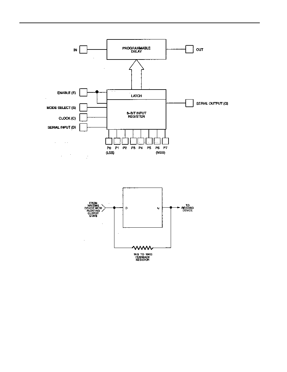
Applications can read the setting of the DS1021 delay line by connecting the serial output pin (Q) to the
serial input (D) through a resistor with a value of 1K to 10K ohms (Figure 2). Since the read process is
destructive, the resistor restores the value read and provides isolation when writing to the device. The
resistor must connect the serial output (Q) of the last device to the serial input (D) of the first device of a
daisy-chain (Figure 3). For serial readout with automatic restoration through a resistor, the device used to
write serial data must go to a high impedance state.
To initiate a serial read, enable (E) is taken to a logic 1 while serial clock (C) is at a logic 0. After a
waiting time (t
EQV
), bit 7 (MSB) appears on the serial output (Q). On the first rising (0 1) transition of
the serial clock (C), bit 7 (MSB) is rewritten and bit 6 appears on the output after a time t
CQV
. To restore
the input register to its original state, this clocking process must be repeated eight times. In the case of a
daisy-chain, the process must be repeated eight times per package. If the value read is restored before
enable (E) is returned to logic 0, no settling time (t
EDV
) is required and the programmed delay remains
unchanged.
Since the DS1021 is a CMOS design, unused input pins (P1 - P7) must be connected to well-defined logic
levels; they must not be allowed to float. Serial output Q/P0 should be allowed to float if unused.

DS1021
4 of 9
CASCADING MULTIPLE DEVICES (DAISY CHAIN) Figure 3
PART NUMBER TABLE Table 1
DELAYS AND TOLERANCES (IN ns)
PART NUMBER
STEP ZERO
DELAY TIME
MAX DELAY
TIME (NOM)
DELAY CHANGE
PER STEP (NOM)
MAX DEVIATION FROM
PROGRAMMED DELAY
DS1020-25
10 ± 2
73.75
0.25
±6
DS1020-50
10 ± 2
137.5
0.5
±8
DELAY VS. PROGRAMMED VALUE Table 2
MI
N
DELAY
(STEP ZERO)
MAX
DELAY
PARALLEL
PO
RT
S
E
RIAL
PO
RT
0
0
0
0
0
0
1
1
1
P7
MSB
0
0
0
0
0
0
1
1
1
P6
BINARY
PROGRAMMED
VALUE
0
0
0
0
0
0
1
1
1
P5
0
0
0
0
0
0
1
1
1
P4
0
0
0
0
0
0
1
1
1
P3
0
0
0
0
1
1
1
1
1
P2
0
0
1
1
0
0
0
1
1
P1
PART
NUMBER
0
1
0
1
0
1
1
0
1
P0
LSB
DS1021-25
10.00
10.25
10.50
10.75
11.00
11.25
73.25
73.50
73.75
DS1021-50
10.0
10.5
11.0
11.5
12.0
12.5
136.5
137.0
137.5
All delays in nanoseconds, referenced to input pin.
DS1021
DS1021
DS1021

DS1021
5 of 9
DALLAS SEMICONDUCTOR TEST CIRCUIT Figure 4
TEST SETUP DESCRIPTION
Figure 4 illustrates the hardware configuration used for measuring the timing parameters of the DS1021.
The input waveform is produced by a precision pulse generator under software control. Time delays are
measured by a time interval counter (20 ps resolution) connected to the output. The DS1021 serial and
parallel ports are controlled by interfaces to a central computer. All measurements are fully automated
with each instrument controlled by the computer over an IEEE 488 bus.
TEST CONDITIONS
INPUT:
Ambient Temperature:
25°C ± 3°C
Supply Voltage (V
CC
):
5.0V ± 0.1V
Input Pulse:
High = 3.0V ± 0.1V
Low = 0.0V ± 0.1V
Source Impedance:
50 ohms max.
Rise and Fall Time:
3.0 ns max.
(measured between 0.6V and 2.4V)
Pulse Width:
500 ns (DS102125)
2 µs (DS102150)
Period:
1 µs (DS102125)
4 µs (DS102150)
NOTE: Above conditions are for test only and do not restrict the operation of the device under other data
sheet conditions.
OUTPUT:
Output is loaded with a 74F04. Delay is measured between the 1.5V level of the rising edge of the input
signal and the 1.5V level of the corresponding edge of the output.
DS1021