
1 of 5
111799
FEATURES
All-silicon time delay
5 taps equally spaced
Delays are stable and precise
Both leading and trailing edge accuracy
Delay tolerance
±
5% or
±
2 ns, whichever is
greater
Low-power CMOS
TTL/CMOS-compatible
Vapor phase, IR and wave solderable
Custom delays available
Fast turn prototypes
Extended temperature range available
(DS1000-IND)
PIN ASSIGNMENT
PIN DESCRIPTION
TAP 1-TAP 5 - TAP Output Number
V
CC
- +5 Volts
GND
- Ground
NC
- No Connection
IN
- Input
DESCRIPTION
The DS1000 series delay lines have five equally spaced taps providing delays from 4 ns to 500 ns. These
devices are offered in a standard 14-pin DIP that is pin-compatible with hybrid delay lines. Alternatively,
8-pin DIPs and surface mount packages are available to save PC board area. Low cost and superior
reliability over hybrid technology is achieved by the combination of a 100% silicon delay line and
industry standard DIP and SOIC packaging. In order to maintain complete pin compatibility, DIP
packages are available with hybrid lead configurations. The DS1000 series delay lines provide a nominal
accuracy of
±
5% or
±
2 ns, whichever is greater. The DS1000 5-Tap Silicon Delay Line reproduces the
input logic state at the output after a fixed delay as specified by the extension of the part number after the
dash. The DS1000 is designed to reproduce both leading and trailing edges with equal precision. Each
tap is capable of driving up to ten 74LS loads. Dallas Semiconductor can customize standard products to
meet special needs. For special requests and rapid delivery, call 972-371-4348.
DS1000
5-Tap Silicon Delay Line
www.dalsemi.com
IN
NC
NC
TAP 2
TAP 4
NC
GND
NC
NC
NC
TAP 5
TAP 3
TAP 1
V
CC
1
2
3
4
5
6
7
14
13
12
11
10
9
8
DS1000 14-Pin DIP (300-mil)
See Mech. Drawings Section
IN
TAP 2
TAP 4
GND
V
CC
TAP 1
TAP 3
TAP 5
1
2
3
4
6
5
8
7
DS1000M 8-Pin DIP (300-mil)
See Mech. Drawings Section
IN
TAP 2
TAP 4
GND
V
CC
TAP 1
TAP 3
TAP 5
1
2
3
4
6
5
8
7
DS1000Z 8-Pin SOIC (150-mil)
See Mech. Drawings Section

DS1000
2 of 5
LOGIC DIAGRAM Figure 1
DS1000
PART NUMBER DELAY TABLE (all values in ns) Table 1
TAP 1
TAP 2
TAP 3
TAP 4
TAP 5
TOLERANCE
TOLERANCE
TOLERANCE
TOLERANCE
TOLERANCE
PART #
DS1000-
Nom
Init
Temp
Nom
Init
Temp
Nom
Init
Temp
Nom
Init
Temp
Nom
Init
Temp
-20
4
2
1
8
2
1
12
2
1
16
2
1
20
2
1
-25
5
2
1
10
2
1
15
2
1
20
2
1
25
2
1
-30
6
2
1
12
2
1
18
2
1
24
2
1
30
2
1
-35
7
2
1
14
2
1
21
2
1
28
2
1
35
2
1.1
-40
8
2
1
16
2
1
24
2
1
32
2
1
40
2
1.2
-45
9
2
1
18
2
1
27
2
1
36
2
1.1
45
2.3
1.4
-50
10
2
1
20
2
1
30
2
1
40
2
1.2
50
2.5
1.5
-60
12
2
1
24
2
1
36
2
1.1
48
2.4
1.5
60
3
1.8
-75
15
2
1
30
2
1
45
2.3
1.4
60
3
1.8
75
3.8
2.3
-100
20
2
1
40
2
1.2
60
3
1.8
80
4
2.4
100
5
3
-125
25
2
1
50
2.5
1.5
75
3.8
2.3
100
5
3
125
6.3
3.8
-150
30
2
1
60
3
1.8
90
4.5
2.7
120
6
3.6
150
7.5
4.5
-175
35
2
1.1
70
3.5
2.1
105
5.3
3.2
140
7
4.2
175
8.8
5.3
-200
40
2
1.2
80
4
2.4
120
6
3.6
160
8
4.8
200
10
6
-250
50
2.5
1.5
100
5
3
150
7.5
4.5
200
10
6
250
12.5
7.5
-500
100
5
3
200
10
6
300
15
9
400
20
12
500
25
15
DC ELECTRICAL CHARACTERISTICS
(0°C to 70°C; V
CC
= 5.0V ± 5%)
PARAMETER
SYM
TEST
CONDITION
MIN
TYP
MAX
UNITS
NOTES
Supply Voltage
V
CC
4.75
5.00
5.25
V
6
High Level Input
Voltage
V
IH
2.2
V
CC
+ 0.5
V
6
Low Level Input
Voltage
V
IL
-0.5
0.8
V
6
Input Leakage
Current
I
I
0.0V
V
I
V
CC
-1.0
1.0
uA
Active Current
I
CC
V
CC
=Max;
Period=Min.
35
75
mA
7, 9
High Level Output
Current
I
OH
V
CC
=Min.
V
OH
=4
-1
mA
Low Level Output
Current
I
OL
V
CC
=Min.
V
OL
=0.5
12
mA
AC ELECTRICAL CHARACTERISTICS
(T
A
= 25°C; V
CC
= 5V ± 5%)
PARAMETER
SYMBOL
MIN
TYP
MAX
UNITS
NOTES
Input Pulse Width
t
WI
40% of Tap 5 t
PLH
ns
8
Input to Tap Delay
(leading edge)
t
PLH
Table 1
ns
1, 2, 3, 4,
5, 10
Input to Tap Delay
(trailing edge)
t
PHL
Table 1
ns
1, 2, 3, 4,
5, 10
Power-up Time
t
PU
100
ms
Input Period
Period
4 (t
WI
)
ns
8

DS1000
3 of 5
CAPACITANCE
(T
A
= 25°C)
PARAMETER
SYMBOL
MIN
TYP
MAX
UNITS
NOTES
Input Capacitance
C
IN
5
10
pF
NOTES:
1.
Initial tolerances are
±
=with respect to the nominal value at 25
°
C and 5V.
2.
Temperature tolerance is
±
=with respect to the initial delay value over a range of 0
°
C to 70
°
C.
3.
The delay will also vary with supply voltage, typically by less than 4% over the range 4.75 to 5.25V.
4.
All tap delays tend to vary uni-directionally with temperature or voltage changes. For example, if
TAP 1 slows down, all other taps also slow down; TAP3 can never be faster than TAP2.
5.
Intermediate delay values and packaging variations are available on a custom basis. For further
information, call 972-3714348.
6.
All voltages are referenced to ground.
7.
Measured with outputs open.
8.
Pulse width and period specifications may be exceeded; however, accuracy may be impaired
depending on application (decoupling, layout, etc.). The device will remain functional with pulse
widths down to 20% of Tap 5 delay, and input periods as short as 2(t
WI
).
9.
I
CC
is a function of frequency and TAP 5 delay. Only a -25 operating with a 40-ns period and V
CC
=
5.25V will have an I
CC
= 75 mA. For example a -100 will never exceed 30 mA, etc.
10.
See "Test Conditions" section at the end of this data sheet.
TIMING DIAGRAM: SILICON DELAY LINE Figure 2
DS1000
4 of 5
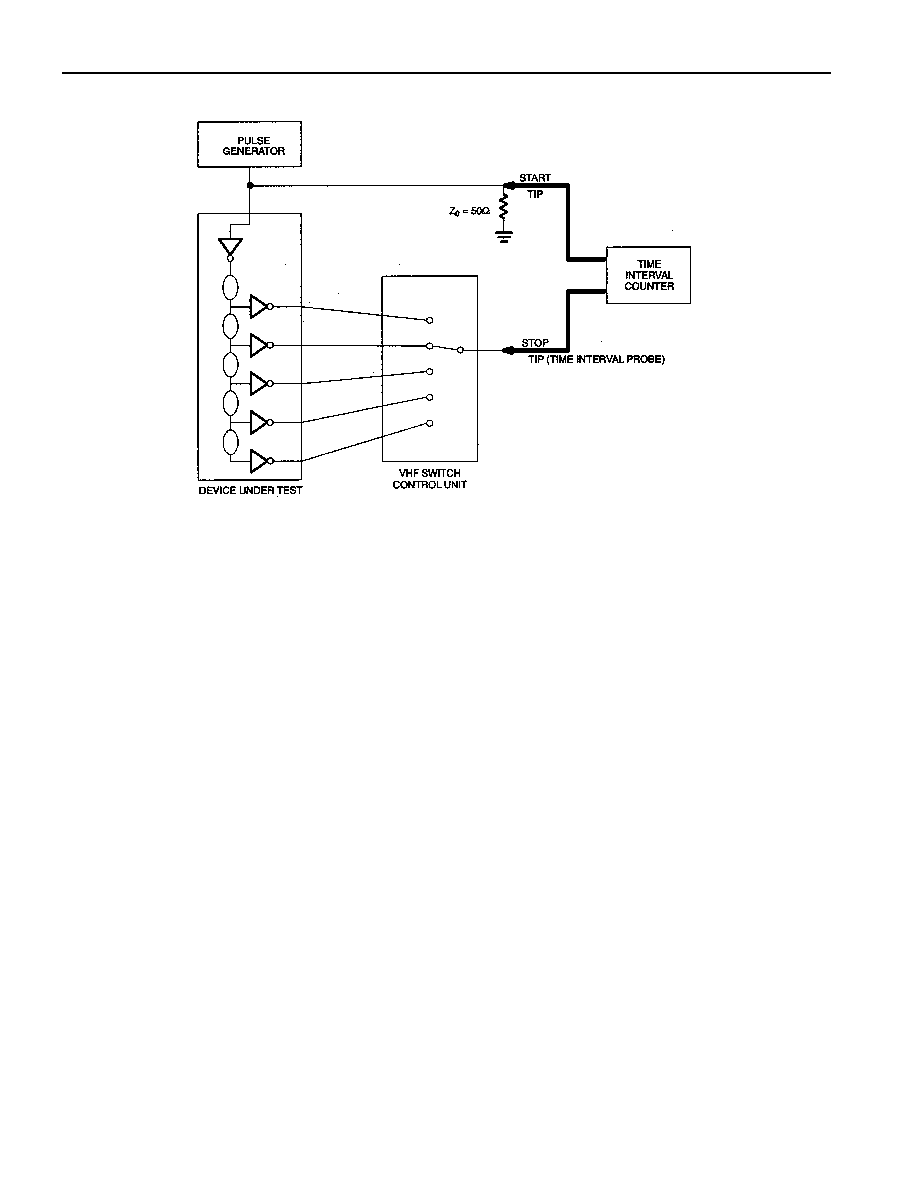
TEST CIRCUIT Figure 3
TERMINOLOGY
Period: The time elapsed between the leading edge of the first pulse and the leading edge of the
following pulse.
t
WI
(Pulse Width):
The elapsed time on the pulse between the 1.5V point on the leading edge and the
1.5V point on the trailing edge or the 1.5V point on the trailing edge and the 1.5V point on the leading
edge.
t
RISE
(Input Rise Time):
The elapsed time between the 20% and the 80% point on the leading edge of the
input pulse.
t
FALL
(Input Fall Time):
The elapsed time between the 80% and the 20% point on the trailing edge of the
input pulse.
t
PLH
(Time Delay, Rising): The elapsed time between the 1.5V point on the leading edge of the input
pulse and the 1.5V point on the leading edge of any tap output pulse.
t
PHL
(Time Delay, Falling): The elapsed time between the 1.5V point on the trailing edge of the input
pulse and the 1.5V point on the trailing edge of any tap output pulse.
TEST SETUP DESCRIPTION
Figure 3 illustrates the hardware configuration used for measuring the timing parameters on the DS1000.
The input waveform is produced by a precision pulse generator under software control. Time delays are
measured by a time interval counter (20 ps resolution) connected between the input and each tap. Each
tap is selected and connected to the counter by a VHF switch control unit. All measurements are fully
automated, with each instrument controlled by a central computer over an IEEE 488 bus.

DS1000
5 of 5
TEST CONDITIONS
INPUT:
Ambient Temperature:
25
°
C
±
=3
°
C
Supply Voltage (V
CC
):
5.0V
±
=0.1V
Input Pulse:
High = 3.0V
±
=0.1V
Low = 0.0V
±
=0.1V
Source Impedance:
50 ohm Max.
Rise and Fall Time:
3.0 ns Max. (measured between 0.6V and 2.4V)
Pulse Width:
500 ns (1
µ
s for -500)
Period:
1
µ
s (2
µ
s for -500)
OUTPUT:
Each output is loaded with the equivalent of one 74F04 input gate. Delay is measured at the 1.5V level on
the rising and falling edge.
NOTE:
Above conditions are for test only and do not restrict the operation of the device under other data sheet
conditions.