Äîêóìåíòàöèÿ è îïèñàíèÿ www.docs.chipfind.ru
2.5V/3.3V, 200 MHz Multi-Output Zero Delay Buffer
Z9960
Cypress Semiconductor Corporation
·
3901 North First Street
·
San Jose
,
CA 95134
·
408-943-2600
Document #: 38-07087 Rev. *C
Revised May 03, 2004
Features
· 2.5V or 3.3V operation
· Output frequency up to 200 MHz
· Supports PowerPC
, and Pentium® processors
· 21 clock outputs: drive up to 42 clock lines
· LVPECL or LVCMOS/LVTTL clock input
· Output-to-output skew < 150 ps
· Split 2.5V/3.3V outputs
· Spread spectrum compatible
· Glitch-free output clocks transitioning
· Output disable control
· Pin-compatible with MPC9600
· Industrial temperature range: 40°C to +85°C
· 48-pin LQFP package
Note:
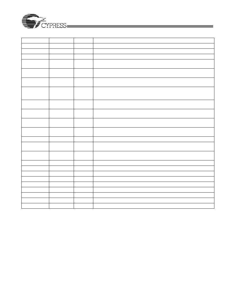
1. Input frequency range: 16 MHz to 33 MHz (FB_SEL = 1), or 25 MHz to 50 MHz (FB_SEL = 0).
Table 1. Frequency Table
[1]
S
E
L
A
QA
S
E
L
B
QB
S
E
L
C
QC
F
B
_
S
E
L
FB_OUT
0
VCO/2
0
VCO/2
0
VCO/2 0
VCO/8
1
VCO/4
1
VCO/4
1
VCO/4 1
VCO/12
/2
/4
/8
/12
REF_SEL
TCLK
PECL_CLK
PECL_CLK#
FB_IN
SELA
SELB
SELC
FB_SEL
OE#
FB_OUT
6
5
4
3
2
1
0
6
5
4
3
2
1
0
6
5
4
3
2
1
0
D Q
D Q
D Q
D Q
0
1
0
1
0
1
0
1
FB
C
B
A
0
1
REF
FB
0
1
AVDD
PLL
Z9960
1
2
3
4
5
6
7
8
9
10
11
12
36
35
34
33
32
31
30
29
28
27
26
25
48 47 46 45 44 43 42 41 40 39 38 37
13 14 15 16 17 18 19 20 21 22 23 24
VSS
TCLK
PECL_CLK
PECL_CLK#
VDD
REF_SEL
FB_SEL
AVDD
SELA
SELB
SELC
VSSC
VDDC
OE#
QC6
QC5
VSSC
QC4
QC3
VDDC
QC2
QC1
QC0
VSSB
VSS
FB_IN
QA0
QA1
VDDA
QA2
QA3
VSSA
QA4
QA5
QA6
VDDA
VSSA
FB_OUT
QB0
QB1
VDDB
QB2
QB3
VSSB
QB4
QB5
QB6
VDDB
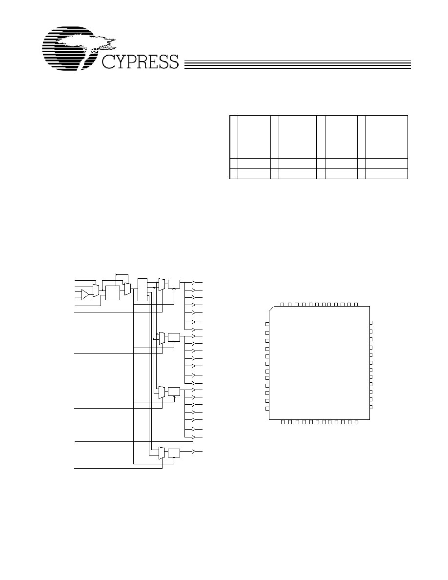
Pin Configuration
Block Diagram
Z9960
Document #: 38-07087 Rev. *C
Page 2 of 7
A bypass capacitor (0.1
µF) should be placed as close as possible to each positive power pin (< 0.2"). If these bypass capacitors
are not close to the pins, their high-frequency filtering characteristic will be cancelled by the lead inductance of the traces.
Pin Definition
Pin Name
No.
Type
Pin Description
PECL_CLK
3
I, PD
PECL Clock Input.
PECL_CLK#
4
I, PU
PECL Clock Input.
TCLK
2
I, PD
External Reference/Test Clock Input.
QA(6:0)
38, 39, 40, 42,
43, 45, 46
O
V
DDA
Clock Outputs. See Table 1 for frequency selections.
QB(6:0)
26, 27, 28, 30,
31, 33, 34
O
V
DDB
Clock Outputs. See Table 1 for frequency selections.
QC(6:0)
15, 16, 18, 19,
21, 22, 23
O
V
DDC
Clock Outputs. See Table 1 for frequency selections.
FB_OUT
35
O
V
DD
Feedback Clock Output. Connect to FB_IN for normal operation. The divider
ratio for this output is set by FB_SEL; see Table 1. A bypass delay capacitor at
this output will control Input Reference/ Output Banks phase relationships.
SELA
9
I, PU
Frequency Select Inputs. These inputs select the divider ratio at QA(0:6)
outputs. See Table 1.
SELB
10
I, PU
Frequency Select Inputs. These inputs select the divider ratio at QB(0:6)
outputs. See Table 1.
SELC
11
I, PU
Frequency Select Inputs. These inputs select the divider ratio at QC(0:6)
outputs. See Table 1.
FB_SEL
7
I, PU
Feedback Select Inputs. These inputs select the divide ratio at FB_OUT output.
See Table 1.
FB_IN
47
I, PD
Feedback Clock Input. Connect to FB_OUT for accessing the PLL.
REF_SEL
6
I, PU
Reference Select Input. When high, the PECL clock is selected. And when low,
TCLK is the reference clock.
OE#
14
I, PD
Output Enable Input. When asserted low, enables all of the outputs. When
pulled high, disables to high impedance all of the outputs except FB_OUT.
V
DDA
37, 44
Power Supply for Bank A Clock Buffers.
V
DDB
25, 32
Power Supply for Bank B Clock Buffers.
V
DDC
13, 20
Power Supply for Bank C Clock Buffers.
V
DD
5
Power Supply for Core
AV
DD
8
Power Supply for PLL. When AVDD is set low, PLL is bypassed.
V
SSA
36, 41
Common Ground for Bank A.
V
SSB
24, 29
Common Ground for Bank B.
V
SSC
12, 17
Common Ground for Bank C.
V
SS
1, 48
Common Ground.
Z9960
Document #: 38-07087 Rev. *C
Page 3 of 7
Overview
The Z9960 has an integrated PLL that provides low skew and
low jitter clock outputs for high-performance microprocessors.
Three independent banks of seven outputs as well as an
independent PLL feedback output, FB_OUT, provide excep-
tional flexibility for possible output configurations. The PLL is
ensured stable operation given that the VCO is configured to
run between 200 MHz to 400 MHz. This allows a wide range
of output frequencies up to 200 MHz.
The phase detector compares the input reference clock to the
external feedback input. For normal operation, the external
feedback input, FB_IN, is connected to the feedback output,
FB_OUT. The internal VCO is running at multiples of the input
reference clock set by FB_SEL select inputs; refer to Table 1.
The VCO frequency is then divided down to provide the
required output frequencies.
Zero Delay Buffer
When used as a zero delay buffer the Z9960 will likely be in a
nested clock tree application. For these applications the
Z9960 offers a low-voltage PECL clock input as a PLL
reference. This allows the user to use LVPECL as the primary
clock distribution device to take advantage of its far-superior
skew performance. The Z9960 then can lock onto the LVPECL
reference and translate with near zero delay to low skew
outputs.
By using one of the outputs as a feedback to the PLL, the
propagation delay through the device is eliminated. The PLL
works to align the output edge, with the input reference edge
thus producing a near-zero delay. The reference frequency
affects the static phase offset of the PLL and thus the relative
delay between the inputs and outputs. Because the static
phase offset is a function of the reference clock, the Tpd of the
Z9960 is a function of the configuration used.
Function Table
Control Pin
0
1
REF_SEL
TCLK
PECL_CLK
AVDD
PLL Bypass, Outputs Controlled by OE#
PLL Power
OE#
Outputs Enabled
Outputs Disabled (except FB_OUT)
SELA
Output Bank A at VCO/2
Output Bank A at VCO/4
SELB
Output Bank B at VCO/2
Output Bank B at VCO/4
SELC
Output Bank C at VCO/2
Output Bank C at VCO/4
FB_SEL
Feedback Output at VCO/8
Feedback Output at VCO/12
Z9960
Document #: 38-07087 Rev. *C
Page 4 of 7
Absolute Maximum Ratings
[2]
Input Voltage Relative to V
SS
:...............................V
SS
0.3V
Input Voltage Relative to V
DD
: ............................. V
DD
+ 0.3V
Storage Temperature: .................................-65
°C to + 150°C
Operating Temperature:................................-40
°C to + 85°C
Maximum ESD Protection................................................ 2kV
Maximum Power Supply: ................................................5.5V
Maximum Input Current:
..................................................± 20mA
This device contains circuitry to protect the inputs against
damage due to high static voltages or electric fields; however,
precautions should be taken to avoid application of any
voltage higher than the maximum rated voltages to this circuit.
For proper operation, V
IN
and V
OUT
should be constrained to
the range
V
SS
< (V
IN
or V
OUT
) < V
DD
.
Unused inputs must always be tied to an appropriate logic
voltage level (either V
SS
or V
DD
).
Note:
2. The voltage on any input or I/O or pin cannot exceed the power pin during power-up. Power supply sequencing is NOT required.
DC Electrical Characteristics V
DD
= 2.5V ±5%, T
A
= 40
°C to +85°C
Parameter
Description
Test Condition
Min.
Typ.
Max.
Unit
V
IL
[3]
Input Low Voltage
V
SS
0.7
V
V
IH
[3]
Input High Voltage
1.7
V
DD
V
V
PP
Peak-to-Peak Input Voltage
PECL_CLK
500
1000
mV
VCMR
[4]
Common Mode Range
PECL_CLK
V
DD
1.4
V
DD
0.6
V
I
IL
[5]
Input Low Current (@ V
IL
= V
SS
)
120
µA
I
IH
[5]
Input High Current (@ V
IH
=
V
DD
)
120
µA
V
OL
[6]
Output Low Voltage
I
OL
= 15 mA
0.6
V
V
OH
[6]
Output High Voltage
I
OH
= 15 mA
1.8
V
I
DD
Quiescent Supply Current
V
DD
and AV
DD
10
13
mA
C
IN
Input Pin Capacitance
4
pF
DC Electrical Characteristics V
DD
= 3.3V +5%, T
A
= 40
°C to +85°C
Parameter
Description
Test Condition
Min.
Typ.
Max.
Unit
V
IL
[3]
Input Low Voltage
V
SS
0.8
V
V
IH
[3]
Input High Voltage
2.0
V
DD
V
V
PP
Peak-to-Peak Input Voltage
PECL_CLK
500
1000
mV
VCMR
[4]
Common Mode Range PECL_CLK
V
DD
1.4
V
DD
0.6
V
I
IL
[5]
Input Low Current (@ V
IL
= V
SS
)
120
µA
I
IH
[5]
Input High Current (@ V
IH
= V
DD
)
120
µA
V
OL
[6]
Output Low Voltage
I
OL
= 24 mA
0.55
V
V
OH
[6]
Output High Voltage
I
OH
= 24 mA
2.4
V
I
DD
Quiescent Supply Current
V
DD
and AV
DD
15
20
mA
C
IN
Input Pin Capacitance
4
pF
Notes:
3. The LVCMOS inputs threshold is at 30% of V
DD
.
4. The VCMR is the difference from the most positive side of the differential input signal. Normal operation is obtained when HIGH input is within the VCMR range
and the input lies within the V
PP
specification.
5. Inputs have pull-up/pull-down resistors that affect input current.
6. Driving series or parallel terminated 50
(or 50 to V
DD
/2) transmission lines.
Z9960
Document #: 38-07087 Rev. *C
Page 5 of 7
AC Electrical Characteristics
V
DD
= 2.5V ±5% or 3.3V ±5%, T
A
= 40
°C to +85°C
[7]
Symbol
Parameter
Test Condition
Min.
Typ.
Max.
Unit
Fref
Reference Input Frequency
FB_SEL = 1
16
33
MHz
FB_SEL = 0
25
50
FrefDC
Reference Input Duty Cycle
25
75
%
Fvco
PLL VCO Lock Range
200
400
MHz
Tlock
Maximum PLL lock Time
10
ms
Tr / Tf
Output Clocks Rise / Fall
Time
[8],[9]
0.55V to 2.0V, V
DD
= 3.3V
0.1
1.0
ns
0.5V to 1.8V, V
DD
= 2.5V
Fout
Maximum Output Frequency
Q (÷2)
100
200
MHz
Q (÷4)
50
100
FoutDC
Output Duty Cycle
[8],[9]
45
50
55
%
tpZL, tpZH
Output Enable Time
[8]
(all
outputs)
2
10
ns
tpLZ, tpHZ
Output Disable Time
[8]
(all
outputs)
2
8
ns
TCCJ
Cycle to Cycle Jitter
[8],[9]
±100
ps
Tskew
Any Output to Any Output
Skew
[8],[9]
Same frequency
150
ps
Different frequency
300
Tskew
Bank to Bank Skew
Banks at different voltages
400
ps
Tskew(pp)
Part to Part Skew
[10]
450
ps
Tpd
Phase
Error
[8],[9]
TCLK or
PECL_CLK to
FB_IN
V
DD
= 3.3V
0
100
200
ps
V
DD
= 2.5V
25
125
225
Note:
7. Parameters are guaranteed by design and characterization. Not 100% tested in production.
8. Outputs loaded with 30pF each.
9. 50
transmission line terminated into VDD/2.
10. Part to Part skew at a given temperature and voltage