DATASHEET SEARCH SITE | WWW.ALLDATASHEET.COM
EZ-USB SX2TM High-Speed USB Interface Device
CY7C68001
Cypress Semiconductor Corporation
·
3901 North First Street
·
San Jose
·
CA 95134
·
408-943-2600
Document #: 38-08013 Rev. *E
Revised July 13, 2004
1.0
EZ-USB SX2TM Features
· USB 2.0-certified compliant
-- On the USB-IF Integrators List: Test ID Number
40000713
· Operates at high (480 Mbps) or full (12 Mbps) speed
· Supports Control Endpoint 0:
-- Used for handling USB device requests
· Supports four configurable endpoints that share a 4-
KB FIFO space
-- Endpoints 2, 4, 6, 8 for application-specific control
and data
· Standard 8- or 16-bit external master interface
-- Glueless interface to most standard microproces-
sors DSPs, ASICs, and FPGAs
-- Synchronous or Asynchronous interface
· Integrated phase-locked loop (PLL)
· 3.3V operation, 5V tolerant I/Os
· 56-pin SSOP and QFN package
· Complies with most device class specifications
2.0
Applications
· DSL modems
· ATA interface
· Memory card readers
· Legacy conversion devices
· Cameras
· Scanners
· Home PNA
· Wireless LAN
· MP3 players
· Networking
· Printers
The "Reference Designs" section of the Cypress web site
provides additional tools for typical USB applications. Each
reference design comes complete with firmware source code
and object code, schematics, and documentation. Please see
the Cypress web site at www.cypress.com.
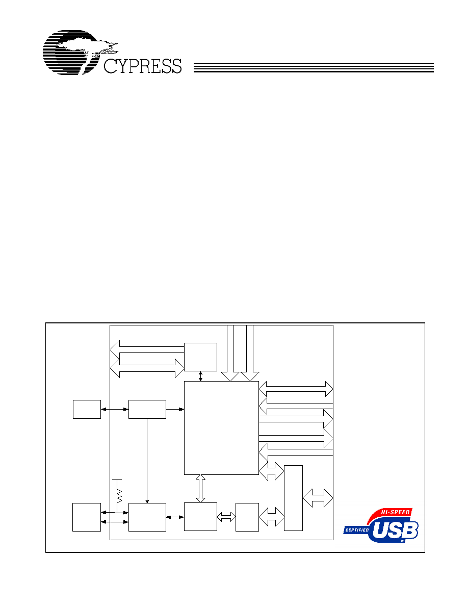
2.1
Block Diagram
SX2 Internal Logic
USB 2.0 XCVR
CY Smart USB
FS/HS Engine
4 KB
FIFO
FIFO
Data
Bus
I2C Bus
Controller
(Master Only)
PLL
24 MHz
XTAL
DPLUS
DMINUS
Data
1.5K
VCC
SCL
SDA
RE
S
E
T
#
Flags (3/4)
Interrupt#, Ready
Control
Address (3)
Read*, Write*, OE*, PKTEND*, CS#
IFCLK*
8/16-Bit Data
WA
K
E
UP
*
Figure 2-1. Block Diagram
CY7C68001
FO R
FO R
Document #: 38-08013 Rev. *E
Page 2 of 42
2.2
Introduction
The EZ-USB SX2
TM
USB interface device is designed to work
with any external master, such as standard microprocessors,
DSPs, ASICs, and FPGAs to enable USB 2.0 support for any
peripheral design. SX2 has a built-in USB transceiver and
Serial Interface Engine (SIE), along with a command decoder
for sending and receiving USB data. The controller has four
endpoints that share a 4-KB FIFO space for maximum flexi-
bility and throughput, as well as Control Endpoint 0. SX2 has
three address pins and a selectable 8- or 16- bit data bus for
command and data input or output.
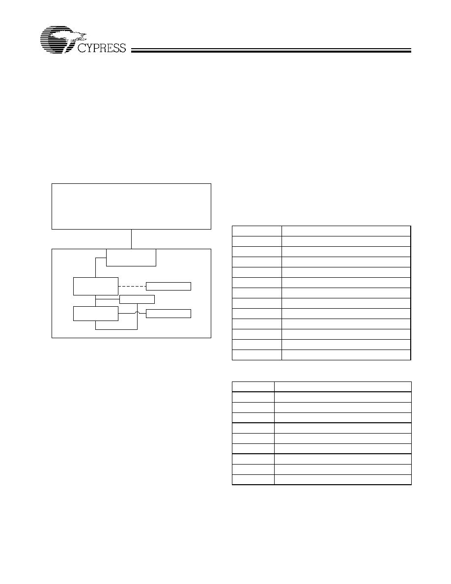
2.3
System Diagram
3.0
Functional Overview
3.1
USB Signaling Speed
SX2 operates at two of the three rates defined in the Universal
Serial Bus Specification Revision 2.0, dated April 27, 2000:
· Full-speed, with a signaling bit rate of 12 Mbits/s
· High-speed, with a signaling bit rate of 480 Mbits/s.
SX2 does not support the low-speed signaling rate of 1.5
Mbits/s.
3.2
Buses
SX2 features:
· A selectable 8- or 16-bit bidirectional data bus
· An address bus for selecting the FIFO or Command Inter-
face.
3.3
Boot Methods
During the power-up sequence, internal logic of the SX2
checks for the presence of an I
2
C EEPROM.
[1,2]
If it finds an
EEPROM, it will boot off the EEPROM. When the presence of
an EEPROM is detected, the SX2 checks the value of first
byte. If the first byte is found to be a 0xC4, the SX2 loads the
next two bytes into the IFCONFIG and POLAR registers,
respectively. If the fourth byte is also 0xC4, the SX2
enumerates using the descriptor in the EEPROM, then signals
to the external master when enumeration is complete via an
ENUMOK interrupt (Section 3.4). If no EEPROM is detected,
the SX2 relies on the external master for the descriptors. Once
this descriptor information is receive from the external master,
the SX2 will connect to the USB bus and enumerate.
3.3.1
EEPROM Organization
The valid sequence of bytes in the EEPROM are displayed
below
Notes:
1.
Because there is no direct way to detect which EEPROM type (single or double address) is connected, SX2 uses the EEPROM address pins A2, A1, and A0
to determine whether to send out one or two bytes of address. Single-byte address EEPROMs (24LC01, etc.) should be strapped to address 000 and double-
byte EEPROMs (24LC64, etc.) should be strapped to address 001.
2.
The SCL and SDA pins must be pulled up for this detection method to work properly, even if an EEPROM is not connected. Typical pull-up values are 2.2K 10K
Ohms.
W ind ow s/U S B C ap ab le H o st
U S B C on ne ction
C ypre ss
S X2
D e vice C PU
A pp licatio n
R A M /R O M
E EP R O M
U S B
C a ble
Figure 2-2. Example USB System Diagram
Table 3-1. Descriptor Length Set to 0x06:
Default Enumeration
Byte Index
Description
0
0xC4
1
IFCONFIG
2
POLAR
3
0xC4
4
Descriptor Length (LSB):0x06
5
Descriptor Length (MSB): 0x00
6
VID (LSB)
7
VID (MSB)
8
PID (LSB)
9
PID (MSB)
10
DID (LSB)
11
DID (MSB)
Table 3-2. Descriptor Length Not Set to 0x06
Byte Index
Description
0
0xC4
1
IFCONFIG
2
POLAR
3
0xC4
4
Descriptor Length (LSB)
5
Descriptor Length (MSB
6
Descriptor[0]
7
Descriptor[1]
8
Descriptor[2]

CY7C68001
FO R
FO R
Document #: 38-08013 Rev. *E
Page 3 of 42
· 0xC4: This initial byte tells the SX2 that this is a valid EE-
PROM with configuration information.
· IFCONFIG: The IFCONFIG byte contains the settings for
the IFCONFIG register. The IFCONFIG register bits are de-
fined in Section 7.1. If the external master requires an in-
terface configuration different from the default, that interface
can be specified by this byte.
· POLAR: The Polar byte contains the polarity of the FIFO
flag pin signals. The POLAR register bits are defined in
Section 7.3. If the external master requires signal polarity
different from the default, the polarity can be specified by
this byte.
· Descriptor: The Descriptor byte determines if the SX2
loads the descriptor from the EEPROM. If this byte = 0xC4,
the SX2 will load the descriptor starting with the next byte.
If this byte does not equal 0xC4, the SX2 will wait for de-
scriptor information from the external master.
· Descriptor Length: The Descriptor length is within the next
two bytes and indicate the length of the descriptor contained
within the EEPROM. The length is loaded least significant
byte (LSB) first, then most significant byte (MSB).
· Byte 7 Starts Descriptor Information: The descriptor can
be a maximum of 500 bytes.
3.3.2
Default Enumeration
An optional default descriptor can be used to simplify enumer-
ation. Only the Vendor ID (VID), Product ID (PID), and Device
ID (DID) need to be loaded by the SX2 for it to enumerate with
this default set-up. This information is either loaded from an
EEPROM in the case when the presence of an EEPROM
(Table 3-1) is detected, or the external master may simply load
a VID, PID, and DID when no EEPROM is present. In this
default enumeration, the SX2 uses the in-built default
descriptor (refer to Section 12.0).
If the descriptor length loaded from the EEPROM is 6, SX2 will
load a VID, PID, and DID from the EEPROM and enumerate.
The VID, PID, and DID are loaded LSB, then MSB. For
example, if the VID, PID, and DID are 0x0547, 0x1002, and
0x0001, respectively, then the bytes should be stored as:
· 0x47, 0x05, 0x02, 0x10, 0x01, 0x00.
If there is no EEPROM, SX2 will wait for the external master
to provide the descriptor information. To use the default
descriptor, the external master must write to the appropriate
register (0x30) with descriptor length equal to 6 followed by the
VID, PID, and DID. Refer to Section 4.2 for further information
on how the external master may load the values.
The default descriptor enumerates four endpoints as listed in
the following page:
· Endpoint 2: Bulk out, 512 bytes in high-speed mode, 64
bytes in full-speed mode
· Endpoint 4: Bulk out, 512 bytes in high-speed mode, 64
bytes in full-speed mode
· Endpoint 6: Bulk in, 512 bytes in high-speed mode, 64 bytes
in full-speed mode
· Endpoint 8: Bulk in, 512 bytes in high-speed mode, 64 bytes
in full-speed mode.
The entire default descriptor is listed in Section 12.0 of this
data sheet.
3.4
Interrupt System
3.4.1
Architecture
The SX2 provides an output signal that indicates to the
external master that the SX2 has an interrupt condition, or that
the data from a register read request is available. The SX2 has
six interrupt sources: SETUP, EP0BUF, FLAGS, ENUMOK,
BUSACTIVITY, and READY. Each interrupt can be enabled or
disabled by setting or clearing the corresponding bit in the
INTENABLE register.
When an interrupt occurs, the INT# pin will be asserted, and
the corresponding bit will be set in the Interrupt Status Byte.
The external master reads the Interrupt Status Byte by
strobing SLRD/SLOE. This presents the Interrupt Status Byte
on the lower portion of the data bus (FD[7:0]). Reading the
Interrupt Status Byte automatically clears the interrupt. Only
one interrupt request will occur at a time; the SX2 buffers
multiple pending interrupts.
If the external master has initiated a register read request, the
SX2 will buffer interrupts until the external master has read the
data. This insures that after a read sequence has begun, the
next interrupt that is received from the SX2 will indicate that
the corresponding data is available. Following is a description
of this INTENABLE register.
3.4.2
INTENABLE Register Bit Definition
Bit 7: SETUP
If this interrupt is enabled, and the SX2 receives a set-up
packet from the USB host, the SX2 asserts the INT# pin and
sets bit 7 in the Interrupt Status Byte. This interrupt only occurs
if the set-up request is not one that the SX2 automatically
handles. For complete details on how to handle the SETUP
interrupt, refer to Section 5.0 of this data sheet.
Bit 6: EP0BUF
If this interrupt is enabled, and the Endpoint 0 buffer becomes
available to the external master for read or write operations,
the SX2 asserts the INT# pin and sets bit 6 in the Interrupt
Status Byte. This interrupt is used for handling the data phase
of a set-up request. For complete details on how to handle the
EP0BUF interrupt, refer to Section 5.0 of this data sheet.
Bit 5: FLAGS
If this interrupt is enabled, and any OUT endpoint FIFO's state
changes from empty to not-empty, the SX2 asserts the INT#
pin and sets bit 5 in the Interrupt Status Byte. This is an
alternate way to monitor the status of OUT endpoint FIFOs
instead of using the FLAGA-FLAGD pins, and can be used to
indicate when an OUT packet has been received from the
host.
Bit 2: ENUMOK
If this interrupt is enabled and the SX2 receives a
SET_CONFIGURATION request from the USB host, the SX2
asserts the INT# pin and sets bit 2 in the Interrupt Status Byte.
This event signals the completion of the SX2 enumeration
process.
Bit 1: BUSACTIVITY
If this interrupt is enabled, and the SX2 detects either an
absence or resumption of activity on the USB bus, the SX2
asserts the INT# pin and sets bit 1 in the Interrupt Status Byte.
This usually indicates that the USB host is either suspending

CY7C68001
FO R
FO R
Document #: 38-08013 Rev. *E
Page 4 of 42
or resuming or that a self-powered device has been plugged
in or unplugged. If the SX2 is bus-powered, the external
master must put the SX2 into a low-power mode after
detecting a USB suspend condition to be USB-compliant.
Bit 0: READY
If this interrupt is enabled, bit 0 in the Interrupt Status Byte is
set when the SX2 has powered up and performed a self-test.
The external master should always wait for this interrupt
before trying to read or write to the SX2, unless an external
EEPROM with a valid descriptor is present. If an external
EEPROM with a valid descriptor is present, the ENUMOK
interrupt will occur instead of the READY interrupt after power
up. A READY interrupt will also occur if the SX2 is awakened
from a low-power mode via the WAKEUP pin. This READY
interrupt indicates that the SX2 is ready for commands or data.
Although it is true that all interrupts will be buffered once a
command read request has been initiated, in very rare condi-
tions, there might be a situation when there is a pending
interrupt already, when a read request is initiated by the
external master. In this case it is the interrupt status byte that
will be output when the external master asserts the SLRD. So,
a condition exists where the Interrupt Status Data Byte can be
mistaken for the result of a command register read request. In
order to get around this possible race condition, the first thing
that the external master must do on getting an interrupt from
the SX2 is check the status of the READY pin. If the READY
is low at the time the INT# was asserted, the data that will be
output when the external master strobes the SLRD is the
interrupt status byte (not the actual data requested). If the
READY pin is high at the time when the interrupt is asserted,
the data output on strobing the SLRD is the actual data byte
requested by the external master. So it is important that the
state of the READY pin be checked at the time the INT# is
asserted to ascertain the cause of the interrupt.
3.5
Resets and Wakeup
3.5.1
Reset
An input pin (RESET#) resets the chip. The internal PLL stabi-
lizes after V
CC
has reached 3.3V. Typically, an external RC
network (R = 100 K Ohms, C = 0.1 uf) is used to provide the
RESET# signal. The Clock must be in a stable state for at least
200 us before the RESET is released.
3.5.2
USB Reset
When the SX2 detects a USB Reset condition on the USB bus,
SX2 handles it like any other enumeration sequence. This
means that SX2 will enumerate again and assert the
ENUMOK interrupt to let the external master know that it has
enumerated. The external master will then be responsible for
configuring the SX2 for the application. The external master
should also check whether SX2 enumerated at High or Full
speed in order to adjust the EPxPKTLENH/L register values
accordingly. The last initialization task is for the external
master to flush all of the SX2 FIFOs.
3.5.3
Wakeup
The SX2 exits its low-power state when one of the following
events occur:
· USB bus signals a resume. The SX2 will assert a BUSAC-
TIVITY interrupt.
· The external master asserts the WAKEUP pin. The SX2 will
assert a READY interrupt
[3]
.
3.6
Endpoint RAM
3.6.1
Size
· Control endpoint: 64 Bytes: 1 × 64 bytes (Endpoint 0).
· FIFO Endpoints: 4096 Bytes: 8 × 512 bytes (Endpoint 2, 4,
6, 8).
3.6.2
Organization
· EP0Bidirectional Endpoint 0, 64-byte buffer.
· EP2, 4, 6, 8Eight 512-byte buffers, bulk, interrupt, or iso-
chronous. EP2 and EP6 can be either double-, triple-, or
quad-buffered. EP4 and EP8 can only be double-buffered.
For high-speed endpoint configuration options, see
Figure 3-1.
Note:
3.
if the descriptor loaded is set for remote wakeup enabled and the host does a set feature remote wakeup enabled, then the SX2 logic will perform RESUME
signalling after a WAKEUP interrupt.
CY7C68001
FO R
FO R
Document #: 38-08013 Rev. *E
Page 5 of 42
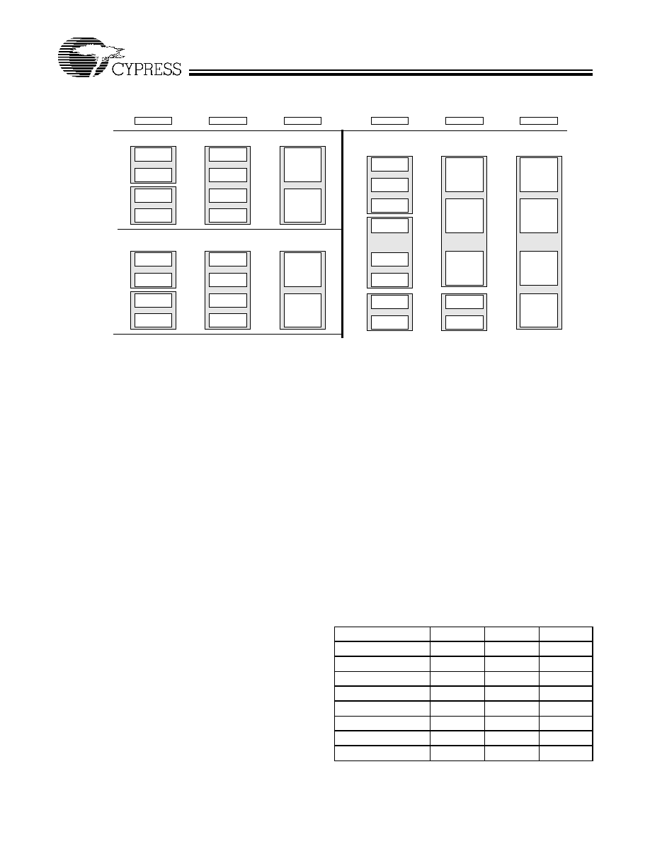
3.6.3
Endpoint Configurations (High-speed Mode)
Endpoint 0 is the same for every configuration as it serves as
the CONTROL endpoint. For Endpoints 2, 4, 6, and 8, refer to
Figure 3-1. Endpoints 2, 4, 6, and 8 may be configured by
choosing either:
· One configuration from Group A and one from Group B
· One configuration from Group C.
Some example endpoint configurations are as follows.
· EP2: 1024 bytes double-buffered, EP6: 512 bytes quad-
buffered.
· EP2: 512 bytes double-buffered, EP4: 512 bytes double-
buffered, EP6: 512 bytes double-buffered, EP8: 512 bytes
double buffered.
· EP2: 1024 bytes quad-buffered.
3.6.4
Default Endpoint Memory Configuration
At power-on-reset, the endpoint memories are configured as
follows:
· EP2: Bulk OUT, 512 bytes/packet, 2x buffered.
· EP4: Bulk OUT, 512 bytes/packet, 2x buffered.
· EP6: Bulk IN, 512 bytes/packet, 2x buffered.
· EP8: Bulk IN, 512 bytes/packet, 2x buffered.
3.7
External Interface
The SX2 presents two interfaces to the external master.
1. A FIFO interface through which EP2, 4, 6, and 8 data flows.
2. A command interface, which is used to set up the SX2, read
status, load descriptors, and access Endpoint 0.
3.7.1
Architecture
The SX2 slave FIFO architecture has eight 512-byte blocks in
the endpoint RAM that directly serve as FIFO memories and
are controlled by FIFO control signals (IFCLK, CS#, SLRD,
SLWR, SLOE, PKTEND, and FIFOADR[2:0]).
The SX2 command interface is used to set up the SX2, read
status, load descriptors, and access Endpoint 0. The
command interface has its own READY signal for gating
writes, and an INT# signal to indicate that the SX2 has data to
be read, or that an interrupt event has occurred. The command
interface uses the same control signals (IFCLK, CS#, SLRD,
SLWR, SLOE, and FIFOADR[2:0]) as the FIFO interface,
except for PKTEND.
3.7.2
Control Signals
3.7.2.1
FIFOADDR Lines
The SX2 has three address pins that are used to select either
the FIFOs or the command interface. The addresses corre-
spond to the following table.
5 1 2
5 1 2
5 1 2
5 1 2
E P 6
E P 8
5 1 2
5 1 2
5 1 2
5 1 2
E P 6
5 1 2
5 1 2
5 1 2
5 1 2
E P 2
5 1 2
5 1 2
E P 6
1 0 2 4
1 0 2 4
E P 6
1 0 2 4
1 0 2 4
E P 2
1 0 2 4
1 0 2 4
1 0 2 4
E P 2
1 0 2 4
1 0 2 4
5 1 2
5 1 2
E P 8
E P 0 I N & O U T
6 4
6 4
6 4
6 4
6 4
6 4
5 1 2
5 1 2
E P 8
G r o u p A
G r o u p C
5 1 2
5 1 2
5 1 2
5 1 2
E P 2
E P 4
5 1 2
5 1 2
5 1 2
5 1 2
E P 2
1 0 2 4
1 0 2 4
E P 2
G r o u p B
Figure 3-1. Endpoint Configuration
Table 3-3. FIFO Address Lines Setting
Address/Selection
FIFOADR2 FIFOADR1 FIFOADR0
FIFO2
0
0
0
FIFO4
0
0
1
FIFO6
0
1
0
FIFO8
0
1
1
COMMAND
1
0
0
RESERVED
1
0
1
RESERVED
1
1
0
RESERVED
1
1
1
Document Outline