Äîêóìåíòàöèÿ è îïèñàíèÿ www.docs.chipfind.ru
32-Macrocell MAX
®
EPLD
CY7C344B
USE ULTRA37000
TM
FOR
ALL NEW DESIGNS
Cypress Semiconductor Corporation
·
3901 North First Street
·
San Jose
,
CA 95134
·
408-943-2600
Document #: 38-03006 Rev. *A
Revised April 19, 2004
Features
· High-performance, high-density replacement for TTL,
74HC, and custom logic
· 32 macrocells, 64 expander product terms in one LAB
· 8 dedicated inputs, 16 I/O pins
· 0.8-micron double-metal CMOS EPROM technology
· 28-pin, 300-mil DIP, cerDIP or 28-pin HLCC, PLCC
package
Functional Description
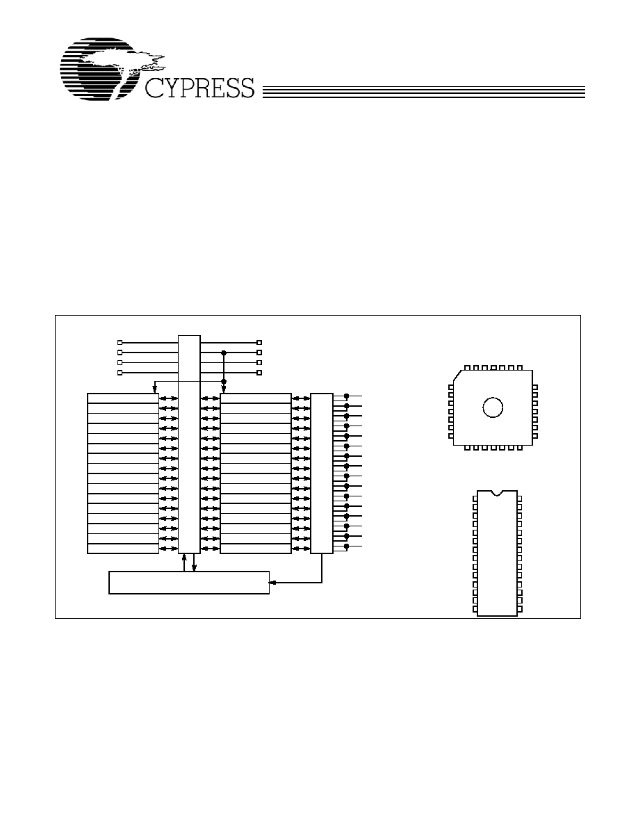
Available in a 28-pin, 300-mil DIP or windowed J-leaded
ceramic chip carrier (HLCC), the CY7C344 represents the
densest EPLD of this size. Eight dedicated inputs and 16
bidirectional I/O pins communicate to one logic array block. In
the CY7C344 LAB there are 32 macrocells and 64 expander
product terms. When an I/O macrocell is used as an input, two
expanders are used to create an input path. Even if all of the
I/O pins are driven by macrocell registers, there are still 16
"buried" registers available. All inputs, macrocells, and I/O pins
are interconnected within the LAB.
The speed and density of the CY7C344 makes it a natural for
all types of applications. With just this one device, the designer
can implement complex state machines, registered logic, and
combinatorial "glue" logic, without using multiple chips. This
architectural flexibility allows the CY7C344 to replace
multichip TTL solutions, whether they are synchronous,
asynchronous, combinatorial, or all three.
Logic Block Diagram
MACROCELL 2
MACROCELL 4
MACROCELL 6
MACROCELL 8
MACROCELL 10
MACROCELL 12
MACROCELL 14
MACROCELL 16
MACROCELL 18
MACROCELL 20
MACROCELL 22
MACROCELL 24
MACROCELL 26
MACROCELL 28
MACROCELL 30
MACROCELL 32
MACROCELL 1
MACROCELL 3
MACROCELL 5
MACROCELL 7
MACROCELL 9
MACROCELL 11
MACROCELL 13
MACROCELL 15
MACROCELL 17
MACROCELL 19
MACROCELL 21
MACROCELL 23
MACROCELL 25
MACROCELL 27
MACROCELL 29
MACROCELL 31
G
L
O
B
A
L
B
U
S
I
O
C
O
N
T
R
O
L
INPUT
INPUT
INPUT
INPUT
15(22)
15(23)
27(6)
28(7)
INPUT
1(8)
INPUT/CLK 2(9)
INPUT
13(20)
INPUT
14(21)
I/O
3(10)
I/O
4(11)
I/O
5(12)
I/O
6(13)
I/O
9(16)
I/O 10(17)
I/O 11(18)
I/O 12(19)
I/O 17(24)
I/O 18(25)
I/O 19(26)
I/O 20(27)
I/O
23(2)
I/O
24(3)
I/O
25(4)
I/O
26(5)
64 EXPANDER PRODUCT TERM ARRAY
32
Pin Configurations
Top View
HLCC
25
24
23
22
21
20
19
5
6
7
8
9
10
11
12 13 14 1516 1718
4 3 2
28 27 26
I/O
I/O
INPUT
INPUT
INPUT
I/O
I/O
INPUT
INPUT
INPUT/CLK
I/O
I/O
I/O
I/O
I/O
GND
I/O
I/O
I/O
I/O
V CC
1
V CC
INPUT
I/O
GND
I/O
I/O
INPUT
1
2
3
4
5
6
7
8
9
10
11
12
13
14
28
27
26
25
24
23
22
21
20
19
18
17
16
15
INPUT
INPUT
Top View
CerDIP
INPUT/CLK
I/O
I/O
I/O
I/O
V
CC
GND
I/O
I/O
I/O
I/O
INPUT
INPUT
INPUT
I/O
I/O
I/O
I/O
V
CC
GND
I/O
I/O
I/O
I/O
INPUT
INPUT
[1]
CY7C344B
USE ULTRA37000
TM
FOR
ALL NEW DESIGNS
Document #: 38-03006 Rev. *A
Page 2 of 16
Selection Guide
7C344-15
7C344-20
7C344-25
Unit
Maximum Access Time
15
20
25
ns
Maximum Operating Current
Commercial
200
200
200
mA
Military
220
220
Industrial
220
220
220
Maximum Standby Current
Commercial
150
150
150
mA
Military
170
170
Industrial
170
170
170
Note:
1. Numbers in () refer to J-leaded packages.
CY7C344B
USE ULTRA37000
TM
FOR
ALL NEW DESIGNS
Document #: 38-03006 Rev. *A
Page 3 of 16
Maximum Ratings
(Above which the useful life may be impaired. For user guide-
lines, not tested.)
Storage Temperature .................................65
°
C to +150
°
C
Ambient Temperature with
Power Applied...................................................0
°
C to +70
°
C
Maximum Junction Temperature (Under Bias).............150
°
C
Supply Voltage to Ground Potential ............... 2.0V to +7.0V
Maximum Power Dissipation...................................1500 mW
DC V
CC
or GND Current ............................................500 mA
Static Discharge Voltage
(per MIL-STD-883, Method 3015) ............................. >2001V
DC Output Current, per Pin ......................25 mA to +25 mA
DC Input Voltage
[2]
.........................................3.0V to +7.0V
DC Program Voltage................................................... +13.0V
Operating Range
Range
Ambient
Temperature
V
CC
Commercial
0
°
C to +70
°
C
5V
±
5%
Industrial
40
°
C to +85
°
C
5V
±
10%
Military
55
°
C to +125
°
C (Case)
5V
±
10%
Electrical Characteristics
Over the Operating Range
[3]
Parameter
Description
Test Conditions
Min.
Max.
Unit
V
OH
Output HIGH Voltage
V
CC
= Min., I
OH
= 4.0 mA
2.4
V
V
OL
Output LOW Voltage
V
CC
= Min., I
OL
= 8 mA
0.45
V
V
IH
Input HIGH Level
2.2
V
CC
+0.3
V
V
IL
Input LOW Level
0.3
0.8
V
I
IX
Input Current
GND
V
IN
V
CC
10
+10
µ
A
I
OZ
Output Leakage Current
V
O
= V
CC
or GND
40
+40
µ
A
I
OS
Output Short Circuit Current
V
CC
= Max., V
OUT
= 0.5V
[4, 5]
30
90
mA
I
CC1
Power Supply
Current (Standby)
V
I
= V
CC
or GND (No
Load)
Commercial
150
mA
Military/Industrial
170
mA
I
CC2
Power Supply Current
V
I
= V
CC
or GND (No
Load) f = 1.0 MHz
[4,6]
Commercial
200
mA
Military/Industrial
220
mA
t
R
Recommended Input Rise Time
100
ns
t
F
Recommended Input Fall Time
100
ns
Capacitance
Parameter
Description
Test Conditions
Max.
Unit
C
IN
Input Capacitance
V
IN
= 2V, f = 1.0 MHz
10
pF
C
OUT
Output Capacitance
V
OUT
= 2.0V, f = 1.0 MHz
10
pF
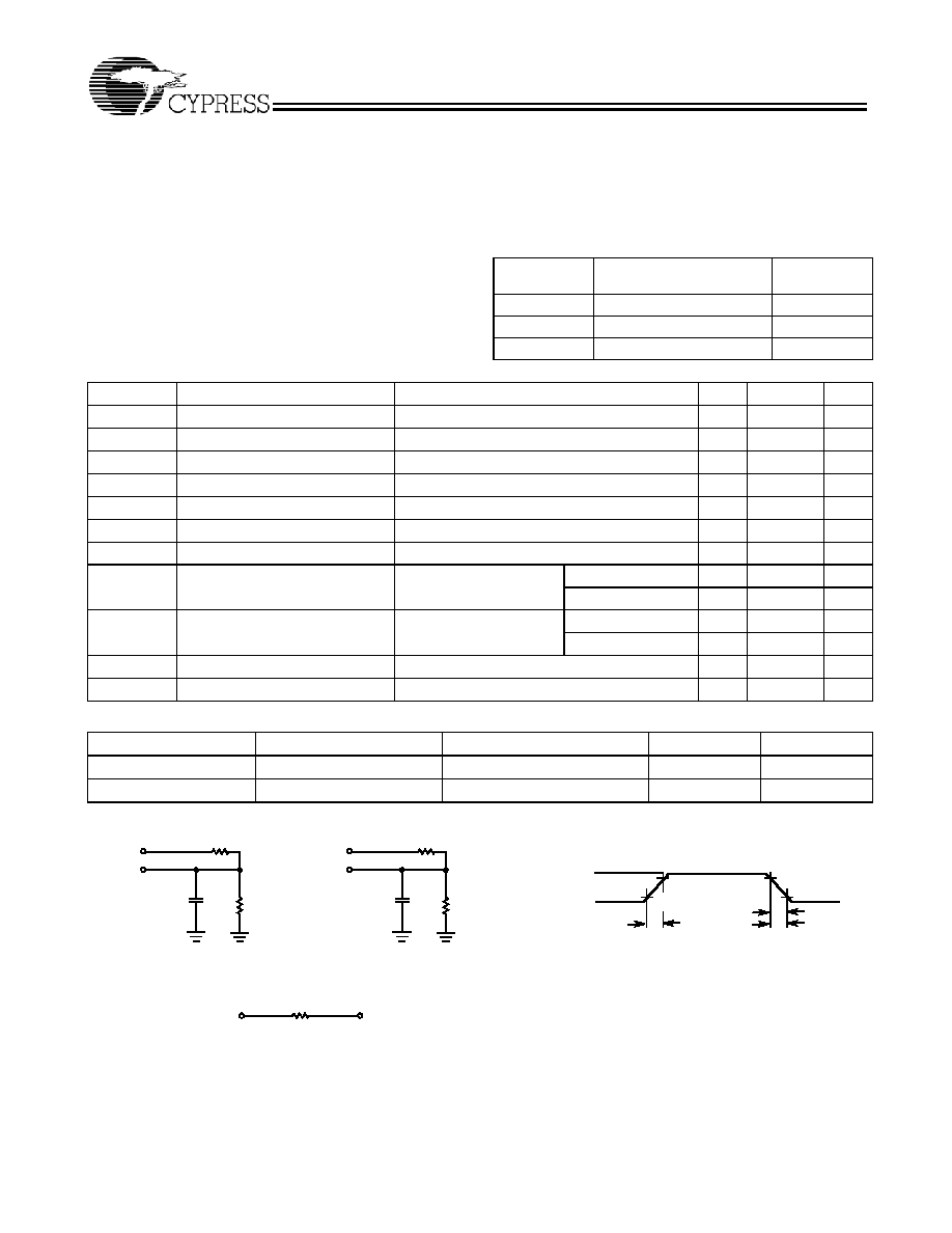
AC Test Loads and Waveforms
[7]
Notes:
2. Minimum DC input is 0.3V. During transitions, the inputs may undershoot to 2.0V for periods less than 20 ns.
3. Typical values are for T
A
= 25
°
C and V
CC
= 5V.
4. Guaranteed by design but not 100% tested.
5. Not more than one output should be tested at a time. Duration of the short circuit should not be more than one second. V
OUT
= 0.5V has been chosen to avoid
test problems caused by tester ground degradation.
6. Measured with device programmed as a 16-bit counter.
7. Part (a) in AC Test Load and Waveforms is used for all parameters except t
ER
and t
XZ
, which is used for part (b) in AC Test Load and Waveforms. All external timing
parameters are measured referenced to external pins of the device.
3.0V
5V
OUTPUT
R1 464
R2
250
50 pF
INCLUDING
JIG AND
SCOPE
GND
90%
10%
90%
10%
6 ns
6 ns
5V
OUTPUT
R1 464
R2
250
(a)
(b)
OUTPUT
1.75V
Equivalent to:
THÉVENIN EQUIVALENT (commercial/military)
ALL INPUT PULSES
t
f
5 pF
t
R
t
F
163
CY7C344B
USE ULTRA37000
TM
FOR
ALL NEW DESIGNS
Document #: 38-03006 Rev. *A
Page 4 of 16
Timing Delays
Timing delays within the CY7C344 may be easily determined
using Warp
®
, Warp ProfessionalTM, or Warp EnterpriseTM
software. The CY7C344 has fixed internal delays, allowing the
user to determine the worst case timing delays for any design.
Design Recommendations
Operation of the devices described herein with conditions
above those listed under "Maximum Ratings" may cause
permanent damage to the device. This is a stress rating only
and functional operation of the device at these or any other
conditions above those indicated in the operational sections of
this data sheet is not implied. Exposure to absolute maximum
ratings conditions for extended periods of time may affect
device reliability. The CY7C344 contains circuitry to protect
device pins from high-static voltages or electric fields; however,
normal precautions should be taken to avoid applying any
voltage higher than maximum rated voltages.
For proper operation, input and output pins must be
constrained to the range GND
(V
IN
or V
OUT
)
V
CC
. Unused
inputs must always be tied to an appropriate logic level (either V
CC
or
GND). Each set of V
CC
and GND pins must be connected together
directly at the device. Power supply decoupling capacitors of at least
0.2
µ
F must be connected between V
CC
and GND. For the most
effective decoupling, each V
CC
pin should be separately decoupled.
Timing Considerations
Unless otherwise stated, propagation delays do not include
expanders. When using expanders, add the maximum
expander delay t
EXP
to the overall delay.
When calculating synchronous frequencies, use t
S1
if all inputs
are on the input pins. t
S2
should be used if data is applied at an I/O
pin. If t
S2
is greater than t
CO1
, 1/t
S2
becomes the limiting frequency
in the data-path mode unless 1/(t
WH
+ t
WL
) is less than 1/t
S2
.
When expander logic is used in the data path, add the appro-
priate maximum expander delay, t
EXP
to t
S1
. Determine which of
1/(t
WH
+ t
WL
), 1/t
CO1
, or 1/(t
EXP
+ t
S1
) is the lowest frequency. The
lowest of these frequencies is the maximum data-path frequency for
the synchronous configuration.
When calculating external asynchronous frequencies, use
t
AS1
if all inputs are on dedicated input pins. If any data is applied to
an I/O pin, t
AS2
must be used as the required set-up time. If (t
AS2
+
t
AH
) is greater than t
ACO1
, 1/(t
AS2
+ t
AH
) becomes the limiting
frequency in the data-path mode unless 1/(t
AWH
+ t
AWL
) is less than
1/(t
AS2
+ t
AH
).
When expander logic is used in the data path, add the appro-
priate maximum expander delay, t
EXP
to t
AS1
. Determine which
of 1/(t
AWH
+ t
AWL
), 1/t
ACO1
, or 1/(t
EXP
+ t
AS1
) is the lowest frequency.
The lowest of these frequencies is the maximum data-path frequency
for the asynchronous configuration.
The parameter t
OH
indicates the system compatibility of this device
when driving other synchronous logic with positive input hold times,
which is controlled by the same synchronous clock. If t
OH
is greater
than the minimum required input hold time of the subsequent
synchronous logic, then the devices are guaranteed to function
properly with a common synchronous clock under worst-case
environmental and supply voltage conditions.
The parameter t
AOH
indicates the system compatibility of this
device when driving subsequent registered logic with a positive hold
time and using the same clock as the CY7C344. In general, if t
AOH
is greater than the minimum required input hold time of the subse-
quent logic (synchronous or asynchronous), then the devices are
guaranteed to function properly under worst-case environmental and
supply voltage conditions, provided the clock signal source is the
same. This also applies if expander logic is used in the clock signal
path of the driving device, but not for the driven device. This is due to
the expander logic in the second device's clock signal path adding an
additional delay (t
EXP
), causing the output data from the preceding
device to change prior to the arrival of the clock signal at the following
device's register.
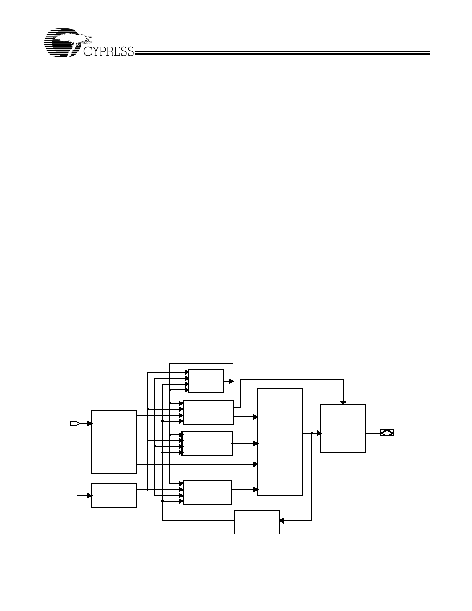
Figure 1. CY7C344 Timing Model
LOGIC ARRAY
CONTROLDELAY
t
LAC
EXPANDER
DELAY
t
EXP
CLOCK
DELAY
t
IC
t
RD
t
COMB
t
LATCH
INPUT
DELAY
t
IN
REGISTER
OUTPUT
DELAY
t
OD
t
XZ
t
ZX
LOGIC ARRAY
DELAY
t
LAD
FEEDBACK
DELAY
t
FD
OUTPUT
INPUT
C3447
SYSTEM CLOCK DELAYt
ICS
t
RH
t
RSU
t
PRE
t
CLR
I/O
I/O DELAY
t
IO
I/O
CY7C344B
USE ULTRA37000
TM
FOR
ALL NEW DESIGNS
Document #: 38-03006 Rev. *A
Page 5 of 16
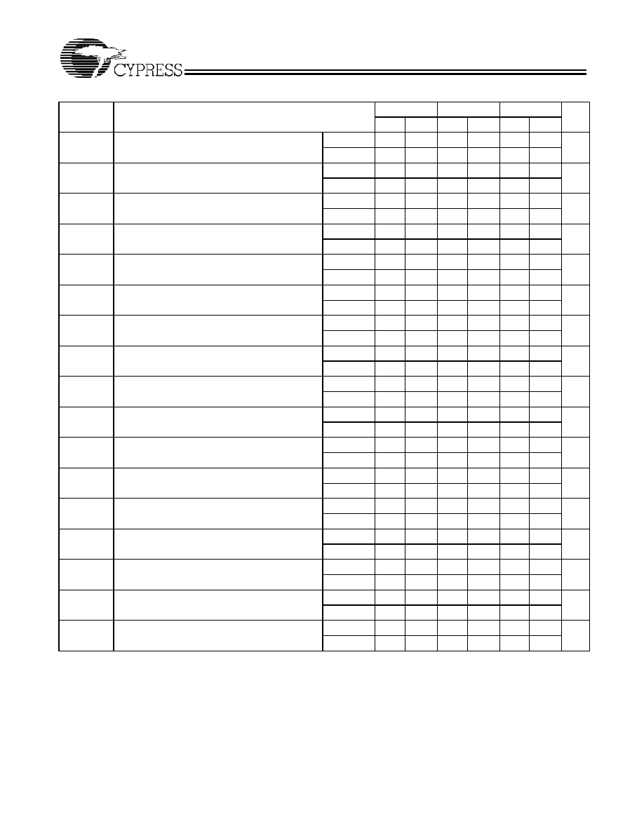
External Synchronous Switching Characteristics
Over Operating Range
[7]
Parameter
Description
7C344-15
7C344-20
7C344-25
Unit
Min.
Max.
Min.
Max.
Min.
Max.
t
PD1
Dedicated Input to Combinatorial Output Delay
[8]
Com'l/Ind
15
20
25
ns
Mil
15
20
25
t
PD2
I/O Input to Combinatorial Output Delay
[9]
Com'l/Ind
15
20
25
ns
Mil
15
20
25
t
PD3
Dedicated Input to Combinatorial Output Delay
with Expander Delay
[10]
Com'l/Ind
30
30
40
ns
Mil
30
30
40
t
PD4
I/O Input to Combinatorial Output Delay with
Expander Delay
[4, 11]
Com'l/Ind
30
30
40
ns
Mil
30
30
40
t
EA
Input to Output Enable Delay
[4]
Com'l/Ind
20
20
25
ns
Mil
20
20
25
t
ER
Input to Output Disable Delay
[4]
Com'l/Ind
20
20
25
ns
Mil
20
20
25
t
CO1
Synchronous Clock Input to Output Delay
Com'l/Ind
10
12
15
ns
Mil
10
12
15
t
CO2
Synchronous Clock to Local Feedback to
Combinatorial Output
[4, 12]
Com'l/Ind
20
22
29
ns
Mil
20
22
29
t
S
Dedicated Input or Feedback Set-Up Time to
Synchronous Clock Input
Com'l/Ind
10
12
15
ns
Mil
10
12
15
t
H
Input Hold Time from Synchronous Clock Input
[7]
Com'l/Ind
0
0
0
ns
Mil
0
0
0
t
WH
Synchronous Clock Input HIGH Time
[4]
Com'l/Ind
6
7
8
ns
Mil
6
7
8
t
WL
Synchronous Clock Input LOW Time
[4]
Com'l/Ind
6
7
8
ns
Mil
6
7
8
t
RW
Asynchronous Clear Width
[4]
Com'l/Ind
20
20
25
ns
Mil
20
20
25
t
RR
Asynchronous Clear Recovery Time
[4]
Com'l/Ind
20
20
25
ns
Mil
20
20
25
t
RO
Asynchronous Clear to Registered Output
Delay
[4]
Com'l/Ind
15
20
25
ns
Mil
15
20
25
t
PW
Asynchronous Preset Width
[4]
Com'l /Ind
20
20
25
ns
Mil
20
20
25
t
PR
Asynchronous Preset Recovery Time
[4]
Com'l /Ind
20
20
25
ns
Mil
20
20
25
Notes:
8. This parameter is the delay from an input signal applied to a dedicated input pin to a combinatorial output on any output pin. This delay assumes no expander
terms are used to form the logic function.
9. This parameter is the delay associated with an input signal applied to an I/O macrocell pin to any output. This delay assumes no expander terms are used to
form the logic function.
10. This parameter is the delay associated with an input signal applied to a dedicated input pin to combinatorial output on any output pin. This delay assumes
expander terms are used to form the logic function and includes the worst-case expander logic delay for one pass through the expander logic. This parameter
is tested periodically by sampling production material.
11. This parameter is the delay associated with an input signal applied to an I/O macrocell pin to any output pin. This delay assumes expander terms are used to
form the logic function and includes the worst-case expander logic delay for one pass through the expander logic. This parameter is tested periodically by
sampling production material.
12. This specification is a measure of the delay from synchronous register clock input to internal feedback of the register output signal to a combinatorial output for
which the registered output signal is used as an input. This parameter assumes no expanders are used in the logic of the combinatorial output and the register
is synchronously clocked. This parameter is tested periodically by sampling production material.