Äîêóìåíòàöèÿ è îïèñàíèÿ www.docs.chipfind.ru
SMPTE HOTLink
®
Transmitter/Receiver
CY7B9234
CY7B9334
Cypress Semiconductor Corporation
·
3901 North First Street
·
San Jose
,
CA 95134
·
408-943-2600
Document #: 38-02014 Rev. *A
Revised April 27, 2004
Features
· SMPTE-259M-CD compliant along with SMPTE-259M
encoder (CY7C9235) and decoder (CY7C9335)
· Fibre Channel compliant
· DVB-ASI compliant
· RX PLL tolerant of long run length data patterns (>20
bits)
· 8B/10B-coded or 10-bit unencoded
· TTL synchronous I/O
· No external PLL components
· Triple PECL 100K serial outputs
· Dual PECL 100K serial inputs
· Low power: 350 mW (Tx), 650 mW (Rx)
· Compatible with fiber-optic modules, coaxial cable, and
twisted pair media
· Built-In Self-Test
· Single +5V supply
· 28-pin PLCC
· 0.8
µ
BiCMOS
Functional Description
The CY7B9234 SMPTE HOTLink
®
Transmitter and
CY7B9334 SMPTE HOTLink Receiver bolt on to the SMPTE
Scrambler Controller (CY7C9235) and SMPTE
Descrambler/Framer Controller (CY7C9335) completing the
four piece chipset to transfer uncompressed SMPTE-259M
encoded video over high-speed serial links (fiber, coax, and
twisted pair). SMPTE HOTLink supports SMPTE-259M-CD
standard data rates at 270 and 360 Mbps. Figure 1 illustrates
typical connections to host systems or controllers.
Eight or ten bits of user data or protocol information are loaded
into the SMPTE HOTLink transmitter and, in DVB mode, are
encoded. Serial data is shifted out of the three differential
positive ECL (PECL) serial ports at the bit rate (which is 10
times the byte rate).
The SMPTE HOTLink receiver accepts the serial bit stream at
its differential line receiver inputs and, using a completely
integrated PLL Clock Synchronizer, recovers the timing infor-
mation necessary for data reconstruction. The bit stream is
deserialized, and in DVB mode, decoded and checked for
transmission errors. Recovered bytes are presented in parallel
to the receiving host along with a byte rate clock.
The 8B/10B encoder/decoder can be disabled in SMPTE or
DVB systems that already encode or scramble the transmitted
data. I/O signals are available to create a seamless interface
with both asynchronous FIFOs (i.e., CY7C42X) and clocked
FIFOs (i.e., CY7C44X). A Built-In Self-Test pattern generator
and checker allows testing of the transmitter, receiver, and the
connecting link as a part of a system diagnostic check.
SMPTE HOTLink devices are ideal for a variety of video appli-
cations including video transmission equipment, video
recorders, video editing equipment, and video routers.
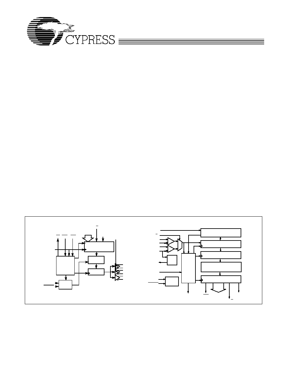
CY7B9234 Transmitter Logic Block Diagram
INPUT REGISTER
D
0
-
7
(D
b
-
h
)
SC/D (D
a
)
SVS(D
j
)
ENABLE
ENCODER
SHIFTER
OUTA
OUTB
OUTC
FOTO
CKW
CLOCK
GENERATOR
ENA
ENN
RP
TEST
LOGIC
MODE
BISTEN
CY7B9334Receiver Logic Block Diagram
RF
A/B
INA+
INB (INB+)
SO
REFCLK
MODE
BISTEN
PECL
TTL
TEST
LOGIC
CLOCK
SYNC
CKR
RDY
SC/D (Q
a
)
RVS(Q
j
)
Q
0
-
7
(Q
b
-
h
)
OUTPUT
REGISTER
DECODER
DECODER
REGISTER
SHIFTER
FRAMER
DATA
INA
-
SI(INB
-
)
CY7B9234
CY7B9334
Document #: 38-02014 Rev. *A
Page 2 of 32
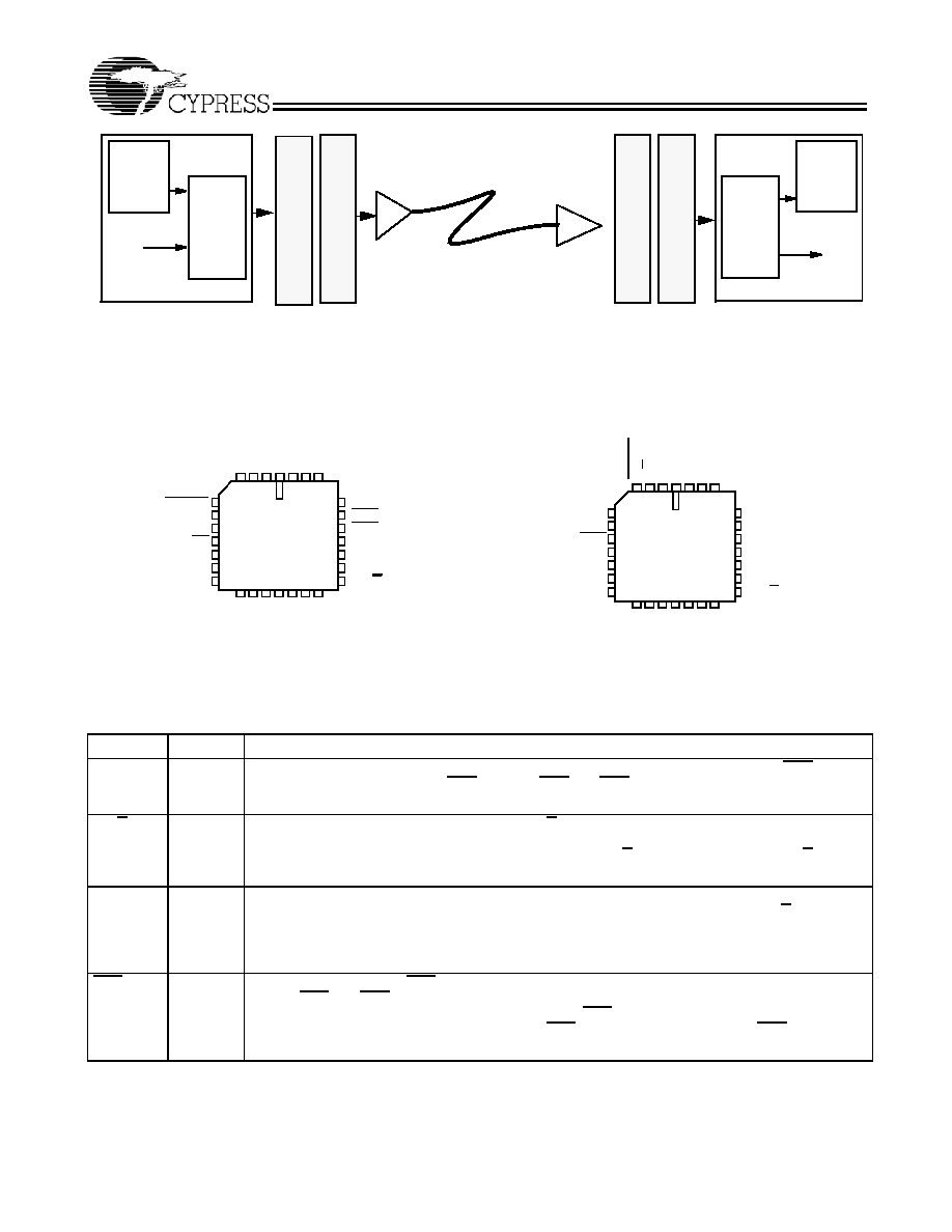
Figure 1. SMPTE HOTLink System Connections
PROT
OCOL
LOGIC
HOST
TRANSMIT
MESSAGE
BUFFER
7B923
4
SERIAL LINK
REC
E
I
V
E
ME
SSAGE
BUFFER
PROT
OCOL
LOGIC
HOST
SMPT
E
E
n
coder
C
Y
7
C
9235
S
M
PTE Serial
izer
CY7B9234
SMPTE Dec
ode
r
CY7C
9335
SMPTE Des
e
ri
aliz
er
CY7B933
4
CY7B9234 Transmitter Pin Configuration
4 3
1
2
28
8
9
7
6
5
22
21
23
24
25
1213
15
14
16
PLCC
Top View
10
11
20
19
2726
1718
FOTO
ENN
ENA
V
CCQ
CKW
GND
SC/D(D
a
)
BISTEN
GND
MODE
RP
V
CCQ
SVS(D
j
)
(D
h
)D
7
6
D
V
OUTC+ OUTC
-
OUTB
+
OUTA
+
OUTA
-
OUTB
-
7B9234
5
D
4
D
3
D
2
D
1
D
0
D
CCN
d
(D
)
e
(D
)
i
(D
)
f
(D
)
g
(D
)
c
(D
)
b
(D
)
CY7B9334 Receiver Pin Configuration
SC/D (Q
a
)
4 3
1
2
28
8
9
7
6
5
22
21
23
24
25
1213
15
14
16
PLCC
Top View
10
11
20
19
2726
1718
REFCLK
V
CCQ
SO
CKR
V
CCQ
GND
RF
GND
RDY
GND
V
CCN
RVS(Q
j
)
(Q
h
) Q
7
Q
Q Q Q
Q Q Q
BISTEN A/B INA+
INB (INB+) SI (I
NB
-
)
MODE
INA
-
7B9334
6
5
4
3
2
1
0
d
(Q
)
e
(Q
)
i
(Q
)
f
(Q
)
g
(Q
)
c
(Q
)
b
(Q
)
Pin Description
CY7B9234 SMPTE HOTLink Transmitter
Name
I/O
Description
D
0
-
7
(D
b
-
h
)
TTL In
Parallel Data Input. Data is clocked into the Transmitter on the rising edge of CKW if ENA is LOW
(or on the next rising CKW with ENN LOW). If ENA and ENN are HIGH, a Null character (K28.5) is
sent. When MODE is HIGH, D
0, 1, ...7
become D
b, c,...h
respectively.
SC/D (D
a
)
TTL In
Special Character/Data Select. A HIGH on SC/D when CKW rises causes the transmitter to encode
the pattern on D
0
-
7
as a control code (Special Character), while a LOW causes the data to be coded
using the 8B/10B data alphabet. When MODE is HIGH, SC/D (D
a
) acts as D
a
input. SC/D has the
same timing as D
0
-
7
.
SVS
(D
j
)
TTL In
Send Violation Symbol. If SVS is HIGH when CKW rises, a Violation symbol is encoded and sent
while the data on the parallel inputs is ignored. If SVS is LOW, the state of D
0
-
7
and SC/D determines
the code sent. In normal or test mode, this pin overrides the BIST generator and forces the trans-
mission of a Violation code. When MODE is HIGH (placing the transmitter in unencoded mode), SVS
(D
j
) acts as the D
j
input. SVS has the same timing as D
0
-
7
.
ENA
TTL In
Enable Parallel Data. If ENA is LOW on the rising edge of CKW, the data is loaded, encoded, and
sent. If ENA and ENN are HIGH, the data inputs are ignored and the Transmitter will insert a Null
character (K28.5) to fill the space between user data. ENA may be held HIGH/LOW continuously or
it may be pulsed with each data byte to be sent. If ENA is being used for data control, ENN will normally
be strapped HIGH, but can be used for BIST function control.
CY7B9234
CY7B9334
Document #: 38-02014 Rev. *A
Page 3 of 32
ENN
TTL In
Enable Next Parallel Data. If ENN is LOW, the data appearing on D
0
-
7
at the next rising edge of
CKW is loaded, encoded, and sent. If ENA and ENN are HIGH, the data appearing on D
0
-
7
at the
next rising edge of CKW will be ignored and the Transmitter will insert a Null character to fill the space
between user data. ENN may be held HIGH/LOW continuously or it may be pulsed with each data
byte sent. If ENN is being used for data control, ENA will normally be strapped HIGH, but can be used
for BIST function control.
CKW
TTL In
Clock Write. CKW is both the clock frequency reference for the multiplying PLL that generates the
high-speed transmit clock, and the byte rate write signal that synchronizes the parallel data input.
CKW must be connected to a crystal controlled time base that runs within the specified frequency
range of the Transmitter and Receiver.
FOTO
TTL In
Fiber-Optic Transmitter Off. FOTO determines the function of two of the three PECL transmitter
output pairs. If FOTO is LOW, the data encoded by the Transmitter will appear at the outputs contin-
uously. If FOTO is HIGH, OUTA
±
and OUTB
±
are forced to their "logic zero" state (OUT+ = LOW and
OUT
-
= HIGH), causing a fiber-optic transmit module to extinguish its light output. OUTC is unaffected
by the level on FOTO, and can be used as a loop-back signal source for board-level diagnostic testing.
OUT A
±
OUT B
±
OUT C
±
PECL Out Differential Serial Data Outputs. These PECL 100K outputs (+5V referenced) are capable of driving
terminated transmission lines or commercial fiber-optic transmitter modules. Unused pairs of outputs
can be wired to V
CC
to reduce power if the output is not required. OUTA
±
and OUTB
±
are controlled by the
level on FOTO, and will remain at their "logical zero" states when FOTO is asserted. OUTC
±
is unaffected by
the level on FOTO (OUTA+ and OUTB+ are used as a differential test clock input while in Test mode, i.e.,
MODE=UNCONNECTED or forced to V
CC
/2).
MODE
3-Level In Encoder Mode Select. The level on MODE determines the encoding method to be used. When wired
to GND, MODE selects 8B/10B encoding. When wired to V
CC
, data inputs bypass the encoder and the
bit pattern on D
aj
goes directly to the shifter. When left floating (internal resistors hold the input at V
CC
/2) the
internal bit-clock generator is disabled and OUTA+/OUTB+ become the differential bit clock to be used for
factory test. In typical applications MODE is wired to V
CC
or GND.
BISTEN
TTL In
Built-In Self-Test Enable. When BISTEN is LOW and ENA and ENN are HIGH, the transmitter sends an
alternating 1
-
0 pattern (D10.2 or D21.5). When either ENA or ENN is set LOW and BISTEN is LOW, the
transmitter begins a repeating test sequence that allows the Transmitter and Receiver to work together to test
the function of the entire link. In normal use this input is held HIGH or wired to V
CC
. The BIST generator is a
free-running pattern generator that need not be initialized, but if required, the BIST sequence can be initialized
by momentarily asserting SVS while BISTEN is LOW. BISTEN has the same timing as D
0
-
7
.
RP
TTL Out
Read Pulse. RP is a 60% LOW duty-cycle byte-rate pulse train suitable for the read pulse in CY7C42X
FIFOs. The frequency on RP is the same as CKW when enabled by ENA, and duty cycle is independent of
the CKW duty cycle. Pulse widths are set by logic internal to the transmitter. In BIST mode, RP will remain
HIGH for all but the last byte of a test loop. RP will pulse LOW one byte time per BIST loop.
V
CCN
Power for output drivers.
V
CCQ
Power for internal circuitry.
GND
Ground.
Pin Description
CY7B9234 SMPTE HOTLink Transmitter (continued)
Name
I/O
Description
Pin Description
CY7B9334 SMPTE HOTLink Receiver
Name
I/O
Description
Q
0
-
7
(Q
b
-
h
)
TTL Out
Q
0
-
7
Parallel Data Output. Q
0
-
7
contain the most recently received data. These outputs change synchro-
nously with CKR. When MODE is HIGH, Q
0, 1, ...7
become Q
b, c,...h
respectively.
SC/D(Q
a
)
TTL Out
Special Character/Data Select. SC/D indicates the context of received data. HIGH indicates a Control
(Special Character) code, LOW indicates a Data character. When MODE is HIGH (placing the receiver in
Unencoded mode), SC/D acts as the Q
a
output. SC/D has the same timing as Q
0
-
7
.
CY7B9234
CY7B9334
Document #: 38-02014 Rev. *A
Page 4 of 32
RVS (Q
j
)
TTL Out
Received Violation Symbol. A HIGH on RVS indicates that a code rule violation has been detected in
the received data stream. A LOW shows that no error has been detected. In BIST mode, a LOW on
RVS indicates correct operation of the Transmitter, Receiver, and link on a byte-by-byte basis. When
MODE is HIGH (placing the receiver in Unencoded mode), RVS acts as the Q
j
output. RVS has the
same timing as Q
0
-
7
.
RDY
TTL Out
Data Output Ready. A LOW pulse on RDY indicates that new data has been received and is ready to be
delivered. A missing pulse on RDY shows that the received data is the Null character (normally inserted by
the transmitter as a pad between data inputs). In BIST mode RDY will remain LOW for all but the last byte of
a test loop and will pulse HIGH one byte time per BIST loop.
CKR
TTL Out
Clock Read. This byte rate clock output is phase and frequency aligned to the incoming serial data
stream. RDY, Q
0
-
7
, SC/D, and RVS all switch synchronously with the rising edge of this output.
A/B
PECL in
Serial Data Input Select. This PECL 100K (+5V referenced) input selects INA or INB as the active
data input. If A/B is HIGH, INA is connected to the shifter and signals connected to INA will be decoded. If
A/B is LOW INB is selected.
INA
±
Diff In
Serial Data Input A. The differential signal at the receiver end of the communication link may be
connected to the differential input pairs INA
±
or INB
±
. Either the INA pair or the INB pair can be used as
the main data input and the other can be used as a loopback channel or as an alternative data input selected
by the state of A/B.
INB
(INB+)
PECL in
(Diff In)
Serial Data Input B. This pin is either a single-ended PECL data receiver (INB) or half of the INB
differential pair. If SO is wired to V
CC
, then INB
±
can be used as differential line receiver interchangeably
with INA
±
. If SO is normally connected and loaded, INB becomes a single-ended PECL 100K (+5V refer-
enced) serial data input. INB is used as the test clock while in Test mode.
SI
(INB
-
)
PECL in
(Diff In)
Status Input. This pin is either a single-ended PECL status monitor input (SI) or half of the INB
differential pair. If SO is wired to V
CC
, then INB
±
can be used as differential line receiver inter-
changeably with INA
±
. If SO is normally connected and loaded, SI becomes a single-ended PECL
100K (+5V referenced) status monitor input, which is translated into a TTL-level signal at the SO pin.
SO
TTL Out
Status Out. SO is the TTL-translated output of SI. It is typically used to translate the Carrier Detect
output from a fiber-optic receiver connected to SI. When this pin is normally connected and loaded
(without any external pull-up resistor), SO will assume the same logical level as SI and INB will become
a single-ended PECL serial data input. If the status monitor translation is not desired, then SO may
be wired to V
CC
and the INB
±
pair may be used as a differential serial data input.
RF
TTL In
Reframe Enable. RF controls the Framer logic in the Receiver. When RF is held HIGH, each SYNC
(K28.5) symbol detected in the shifter will frame the data that follows. If is HIGH for 2,048 consecutive
bytes, the internal framer switches to double-byte mode. When RF is held LOW, the reframing logic
is disabled. The incoming data stream is then continuously deserialized and decoded using byte
boundaries set by the internal byte counter. Bit errors in the data stream will not cause alias SYNC
characters to reframe the data erroneously.
REFCLK
TTL In
Reference Clock. REFCLK is the clock frequency reference for the clock/data synchronizing PLL.
REFCLK sets the approximate center frequency for the internal PLL to track the incoming bit stream.
REFCLK must be connected to a crystal-controlled time base that runs within the frequency limits of
the Tx/Rx pair, and the frequency must be the same as the transmitter CKW frequency (within
CKW
±
0.1%)
MODE
3-Level In Decoder Mode Select. The level on the MODE pin determines the decoding method to be used.
When wired to GND, MODE selects 8B/10B decoding. When wired to V
CC
, registered shifter contents
bypass the decoder and are sent to Q
a
-
j
directly. When left floating (internal resistors hold the MODE pin at
V
CC
/2) the internal bit clock generator is disabled and INB becomes the bit rate test clock to be used for factory
test. In typical applications, MODE is wired to V
CC
or GND.
BISTEN
TTL In
Built-In Self-Test Enable. When BISTEN is LOW the Receiver awaits a D0.0 (sent once per BIST loop)
character and begins a continuous test sequence that tests the functionality of the Transmitter, the Receiver,
and the link connecting them. In BIST mode the status of the test can be monitored with RDY and RVS outputs.
In normal use BISTEN is held HIGH or wired to V
CC
. BISTEN has the same timing as Q
0
-
7
.
V
CCN
Power for output drivers.
V
CCQ
Power for internal circuitry.
GND
Ground.
Pin Description
CY7B9334 SMPTE HOTLink Receiver (continued)
Name
I/O
Description

CY7B9234
CY7B9334
Document #: 38-02014 Rev. *A
Page 5 of 32
CY7B9234 SMPTE HOTLink Transmitter Block
Diagram Description
Input Register
The Input register holds the data to be processed by the
SMPTE HOTLink transmitter and allows the input timing to be
made consistent with standard FIFOs. The Input register is
clocked by CKW and loaded with information on the D
0
-
7
,
SC/D, and SVS pins. Two enable inputs (ENA and ENN) allow the
user to choose when data is loaded in the register. Asserting ENA
(Enable, active LOW) causes the inputs to be loaded in the register
on the rising edge of CKW. If ENN (Enable Next, active LOW) is
asserted when CKW rises, the data present on the inputs on the
next rising edge of CKW will be loaded into the Input register. If
neither ENA nor ENN are asserted LOW on the rising edge of CKW,
then a SYNC (K28.5) character is sent. These two inputs allow
proper timing and function for compatibility with either
asynchronous FIFOs or clocked FIFOs without external logic, as
shown in Figure 5.
In BIST mode, the Input register becomes the signature
pattern generator by logically converting the parallel Input
register into a Linear Feedback Shift Register (LFSR). When
enabled, this LFSR will generate a 511-byte sequence that
includes all Data and Special Character codes, including the
explicit violation symbols. This pattern provides a predictable
but pseudo-random sequence that can be matched to an
identical LFSR in the Receiver.
Encoder
The Encoder transforms the input data held by the Input
register into a form more suitable for transmission on a serial
interface link. The code used is specified by ANSI X3.230
(Fibre Channel), IBM ESCON® channel (code tables are at
the end of this datasheet), and the DVB-ASI serial interface.
The eight D
0
-
7
data inputs are converted to either a Data symbol
or a Special Character, depending upon the state of the SC/D input.
If SC/D is HIGH, the data inputs represent a control code and are
encoded using the Special Character code table. If SC/D is LOW,
the data inputs are converted using the Data code table. If a byte
time passes with the inputs disabled, the Encoder will output a
Special Character Comma K28.5 (or SYNC) that will maintain link
synchronization. SVS input forces the transmission of a specified
Violation symbol to allow the user to check error handling system
logic in the controller or for proprietary applications.
The 8B/10B coding function of the Encoder can be bypassed
for SMPTE systems that include an external coder or
scrambler function as part of the controller. This bypass is
controlled by setting the MODE select pin HIGH. When in
bypass mode, D
a
-
j
(note that bit order is specified in the Fibre
Channel 8B/10B code) become the ten inputs to the Shifter, with D
a
being the first bit to be shifted out.
Shifter
The Shifter accepts parallel data from the Encoder once each
byte time and shifts it to the serial interface output buffers using
a PLL multiplied bit clock that runs at ten (10) times the byte
clock rate. Timing for the parallel transfer is controlled by the
counter included in the Clock Generator and is not affected by
signal levels or timing at the input pins.
OutA, OutB, OutC
The serial interface PECL output buffers (ECL100K refer-
enced to +5V) are the drivers for the serial media. They are all
connected to the Shifter and contain the same serial data. Two
of the output pairs (OUTA
±
and OUTB
±
) are controllable by the
FOTO input and can be disabled by the system controller to force a
logical zero (i.e., "light off") at the outputs. The third output pair
(OUTC
±
) is not affected by FOTO and will supply a continuous data
stream suitable for loop-back testing of the subsystem.
OUTA
±
and OUTB
±
will respond to FOTO input changes within a
few bit times. However, since FOTO is not synchronized with the
transmitter data stream, the outputs will be forced off or turned on at
arbitrary points in a transmitted byte. This function is intended to
augment an external laser safety controller and as an aid for
Receiver PLL testing.
In wire-based systems, control of the outputs may not be
required, and FOTO can be strapped LOW. The three outputs
are intended to add system and architectural flexibility by
offering identical serial bit-streams with separate interfaces for
redundant connections or for multiple destinations. Unneeded
outputs can be wired to V
CC
to disable and power down the
unused output circuitry.
Clock Generator
The clock generator is an embedded phase-locked loop (PLL)
that takes a byte-rate reference clock (CKW) and multiplies it
by ten (10) to create a bit rate clock for driving the serial shifter.
The byte rate reference comes from CKW, the rising edge of
which clocks data into the Input register. This clock must be a
crystal referenced pulse stream that has a frequency between
the minimum and maximum specified for the SMPTE HOTLink
Transmitter/Receiver pair. Signals controlled by this block form
the bit clock and the timing signals that control internal data
transfers between the Input register and the Shifter.
The read pulse (RP) is derived from the feedback counter used in
the PLL multiplier. It is a byte-rate pulse stream with the proper
phase and pulse widths to allow transfer of data from an
asynchronous FIFO. Pulse width is independent of CKW duty
cycle, since proper phase and duty cycle is maintained by the PLL.
The RP pulse stream will insure correct data transfers between
asynchronous FIFOs and the transmitter input latch with no external
logic.
Test Logic
Test logic includes the initialization and control for the Built-In
Self-Test (BIST) generator, the multiplexer for Test mode clock
distribution, and control logic to properly select the data
encoding. Test logic is discussed in more detail in the
CY7B9234 SMPTE HOTLink Transmitter Operating Mode
Description.
CY7B9334 SMPTE HOTLink Receiver Block
Diagram Description
Serial Data Inputs
Two pairs of differential line receivers are the inputs for the
serial data stream. INA
±
or INB
±
can be selected with the A/B
input. INA
±
is selected with A/B HIGH and INB
±
is selected with A/B
LOW. The threshold of A/B is compatible with the ECL 100K signals
from PECL fiber-optic interface modules or active equalizers. TTL
logic elements can be used to select the A or B inputs by adding a
resistor pull-up to the TTL driver connected to A/B. The differential
threshold of INA
±
and INB
±
will accommodate wire interconnect
with filtering losses or transmission line attenuation greater than 20
dB (V
DIF
> 50 mV) or can be directly connected to fiber-optic
interface modules (any ECL logic family, not limited to ECL 100K).
The common mode tolerance will accommodate a wide range of
signal termination voltages. The highest HIGH input that can be