Äîêóìåíòàöèÿ è îïèñàíèÿ www.docs.chipfind.ru
Differential Clock Buffer/Driver
CY2SSTV855
Cypress Semiconductor Corporation
·
3901 North First Street
·
San Jose
,
CA 95134
·
408-943-2600
Document #: 38-07459 Rev. *D
Revised May 07, 2004
Features
· Phase-locked loop (PLL) clock distribution for Double
Data Rate Synchronous DRAM applications
· 1:5 differential outputs
· External feedback pins (FBINT, FBINC) are used to
synchronize the outputs to the clock input
· SSCG: Spread AwareTM for electromagnetic
interference (EMI) reduction
· 28-pin TSSOP package
· Conform to JEDEC DDR specifications
Functional Description
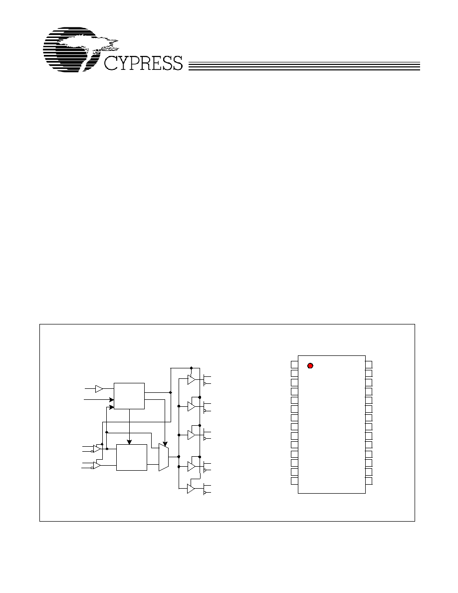
The CY2SSTV855 is a high-performance, very-low-skew,
very-low-jitter zero-delay buffer that distributes a differential
clock input pair (SSTL_2) to four differential (SSTL_2) pairs of
clock outputs and one differential pair of feedback clock
outputs. In support of low power requirements, when
power-down is HIGH, the outputs switch in phase and
frequency with the input clock. When power-down is LOW, all
outputs are disabled to a high-impedance state and the PLL is
shut down.
The device supports a low-frequency power-down mode.
When the input is < 20 MHz, the PLL is disabled and the
outputs are put in the Hi-Z state. When the input frequency is
> 20 MHz, the PLL and outputs are enabled.
When AVDD is tied to ground, the PLL is turned off and
bypassed with the input reference clock gated to the outputs.
The Cypress CY2SSTV855 is Spread Aware and supports
tracking of Spread Spectrum clock inputs to reduce EMI
Block Diagram
Pin Configuration
28 pin TSSOP
1
2
3
4
5
6
7
8
9
10
11
12
13
14
28
27
26
25
24
23
22
21
20
19
18
17
16
15
GND
YT3
VDDQ
FBOUTT
YT2
YC2
GND
VDDQ
FBOUTC
YC3
VDDQ
PWRDWN
FBINT
FBINC
GND
YT0
VDDQ
AGND
YT1
YC1
GND
VDDQ
AVDD
YC0
VDDQ
GND
CLKINT
CLKINC
C
Y
2SSTV855
FBOUTT
FBOUTC
YT0
YC0
YC3
YT3
PLL
PWRDWN
YC2
YT2
YT1
YC1
Powerdown
and test
logic
AVDD
CLKINT
CLKINC
FBINT
FBINC
CY2SSTV855
Document #: 38-07459 Rev. *D
Page 2 of 7
Zero-delay Buffer
When used as a zero-delay buffer the CY2SSTV855 will likely
be in a nested clock tree application. For these applications
the CY2SSTV855 offers a differential clock input pair as a PLL
reference. The CY2SSTV855 then can lock onto the reference
and translate with near zero delay to low-skew outputs. For
normal operation, the external feedback differential input,
FBINT/C, is connected to the feedback output, FBOUTT/C. By
connecting the feedback output to the feedback input the
propagation delay through the device is eliminated. The PLL
works to align the output edge with the input reference edge
thus producing a near zero delay. The reference frequency
affects the static phase offset of the PLL and thus the relative
delay between the inputs and outputs.
When AVDD is strapped LOW, the PLL is turned off and
bypassed for test purposes.
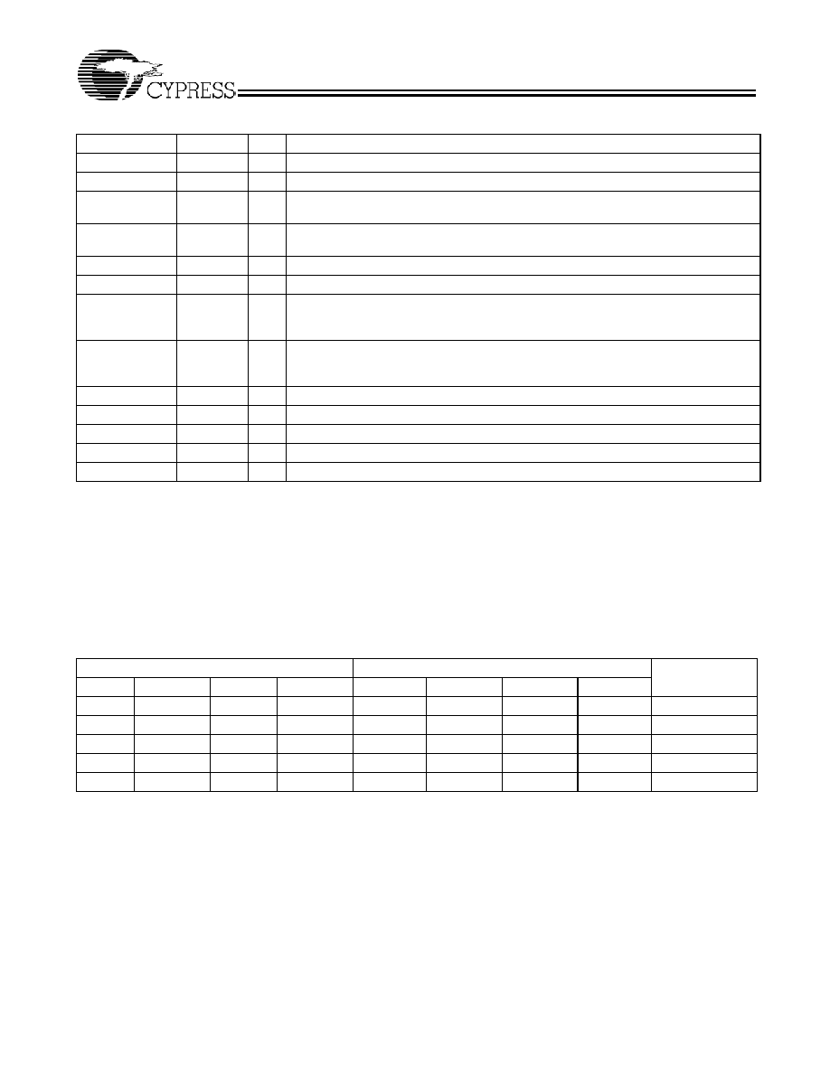
Pin Definition
[1, 2]
Pin
Name
I/O
Description
6
CLKINT
I
True Clock Input. Low Voltage Differential True Clock Input.
7
CLKINC
I
Complementary Clock Input. Low Voltage Differential Complementary Clock Input.
22
FBINC
I
Feedback Complementary Clock Input. Differential Input Connect to FBOUTC for
accessing the PLL.
23
FBINT
I
Feedback True Clock Input. Differential Input Connect to FBOUTT for accessing the
PLL.
3,12,17,26
YT(0:3)
O
True Clock Outputs. Differential Outputs.
2,13,16,27
YC(0:3)
O
Complementary Clock Outputs. Differential Outputs.
19
FBOUTT
O
Feedback True Clock Output. Differential Outputs. Connect to FBINT for normal oper-
ation. A bypass delay capacitor at this output will control Input Reference/Output Clocks
phase relationships.
20
FBOUTC
O
Feedback Complementary Clock Output. Differential Outputs. Connect to FBINC for
normal operation. A bypass delay capacitor at this output will control Input
Reference/Output Clocks phase relationships.
24
PWRDWN
I
Control input to turn device in the power-down mode.
4,8,11,18,21,25
VDDQ
2.5V Power Supply for Output Clock Buffers.2.5V Nominal.
9
AVDD
2.5V Power Supply for PLL. 2.5V Nominal.
1,5,14,15,28
GND
Ground
10
AGND
Analog Ground. 2.5V Analog Ground.
Function Table
Inputs
Outputs
PLL
AVDD
PWRDWN
CLKINT
CLKINC
YT(0:3)
YC(0:3)
FBOUTT
FBOUTC
GND
H
L
H
L
H
L
H
BYPASSED/OFF
GND
H
H
L
H
L
H
L
BYPASSED/OFF
2.5V
H
L
H
L
H
L
H
On
2.5V
H
H
L
H
L
H
L
On
2.5V
X
< 20 MHz
< 20 MHz
Hi-Z
Hi-Z
Hi-Z
Hi-Z
Off
Notes:
1. PU = internal pull-up.
2. A bypass capacitor (0.1
µF) should be placed as close as possible to each positive power pin (< 0.2"). If these bypass capacitors are not close to the pins their
high frequency filtering characteristic will be cancelled by the lead inductance of the traces.
CY2SSTV855
Document #: 38-07459 Rev. *D
Page 3 of 7
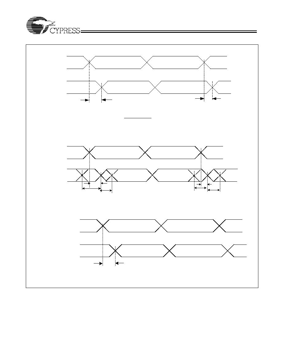
Differential Parameter Measurement Information
t
()
n
t
()
n+1
CLKINT
CLKINC
FBINC
FBINT
N
(
N is large number of samples)
n
n =N
1
t
()
n
t
()
=
Figure 1. Static Phase Offset
td()
td()
t( )
t()
td()
td()
CLKINT
CLKINC
FBINC
FBINT
Figure 2. Dynamic Phase Offset
Y[0:3], FBOUTT
tsk(o)
YC[0:3], FBOUTC
Y[0:3], FBOUTT
YC[0:3], FBOUTC
Figure 3. Output Skew
CY2SSTV855
Document #: 38-07459 Rev. *D
Page 4 of 7
Differential Parameter Measurement Information (continued)
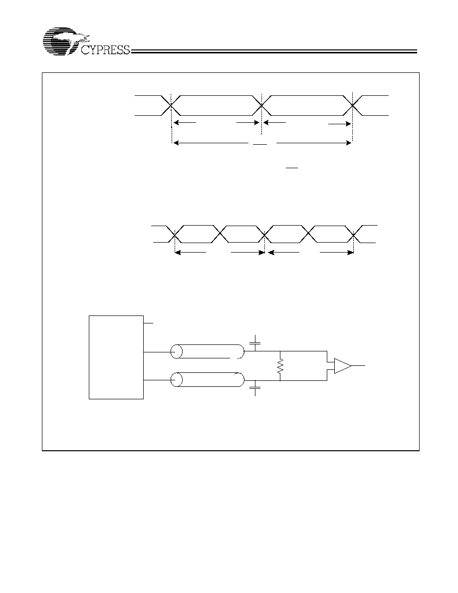
Figure 4. Half-period Jitter
1
f(o)
t
(hper_N+1)
t
(hper_n)
t
jit(hper)
= t
hper(n)
- 1
2x fo
YT[0:3], FBOUTT
YC[0:3], FBOUTC
t
j
it(cc)
= t
c(n)
-t
c(n+1)
YT[0:3], FBOUTT
YC[0:3], FBOUTC
t
c(n)
t
c(n)
Figure 5. Cycle-to-cycle Jitter
6 0 O h m
R e c e ive r
V C P
V T R
R
T
= 1 2 0 O h m
V D D
C L K T
C L K C
V D D
6 0 O h m
1 6 p F
1 6 p F
V D D /2
V D D /2
Figure 6. Differential Signal Using Direct Termination Resistor
CY2SSTV855
Document #: 38-07459 Rev. *D
Page 5 of 7
Absolute Maximum Conditions
[3]
Input Voltage Relative to V
SS
:...............................V
SS
0.3V
Input Voltage Relative to V
DDQ
or AV
DD
: ............. V
DD
+ 0.3V
Storage Temperature: ................................65
°C to + 150°C
Operating Temperature: ................................40
°C to +85°C
Maximum Power Supply: ................................................3.5V
This device contains circuitry to protect the inputs against
damage due to high static voltages or electric field; however,
precautions should be taken to avoid application of any
voltage higher than the maximum rated voltages to this circuit.
For proper operation, V
in
and V
out
should be constrained to the
range:
V
SS
< (V
in
or V
out
) < V
DD
.
Unused inputs must always be tied to an appropriate logic
voltage level (either V
SS
or V
DD
).
DC Electrical Specifications (
AV
DD
= V
DDQ
= 2.5V ± 5%, T
A
= 40°C to +85°C)
[4]
Parameter
Description
Conditions
Min.
Typ.
Max.
Unit
V
ID
Differential Input Voltage
[5]
CLKINT, FBINT
0.36
V
DDQ
+ 0.6
V
V
IX
Differential Input Crossing
Voltage
[6]
CLKTIN, FBINT
(V
DDQ
/2)
0.2
V
DDQ
/2
(V
DDQ
/2) + 0.2
V
I
IN
Input Current
V
IN
= 0V or V
IN
= V
DDQ
, CLKINT,
FBINT
10
10
µA
I
OL
Output Low Current
V
DDQ
= 2.375V, V
OUT
= 1.2V
26
35
mA
I
OH
Output High Current
V
DDQ
= 2.375V, V
OUT
= 1V
18
32
mA
V
OL
Output Low Voltage
V
DDQ
= 2.375V, I
OL
= 12 mA
0.6
V
V
OH
Output High Voltage
V
DDQ
= 2.375V, I
OH
= 12 mA
1.7
V
V
OUT
Output Voltage Swing
[7]
1.1
V
DDQ
0.4
V
V
OC
Output Crossing Voltage
[8]
(V
DDQ
/2) 0.2 V
DDQ
/2
(V
DDQ
/2) + 0.2
V
I
OZ
High-Impedance Output
Current
V
O
= GND or V
O
= V
DDQ
10
10
µA
I
DDQ
Dynamic Supply Current
[9]
V
DDQ
= 170 MHz
235
300
mA
I
DD
PLL Supply Current
AV
DD
only
9
12
mA
Cin
Input Pin Capacitance
4
pF
AC Electrical Specifications (
AV
DD
= V
DDQ
= 2.5V±5%, T
A
= 40°C to +85°C)
[10, 11]
Parameter
Description
Conditions
Min.
Typ.
Max.
Unit
f
CLK
Operating Clock Frequency
AV
DD
= 2.5V
± 0.2V
60
170
MHz
t
DC
Input Clock Duty Cycle
[12]
40
60
%
t
LOCK
Maximum PLL lock Time
100
µs
t
SL(O)
Output Clocks Slew Rate
20% to 80% of VOD
1
2
V/ns
t
PZL
, t
PZH
Output Enable Time (all outputs)
[13]
30
ns
t
PLZ
, t
PHZ
Output Disable Time (all outputs)
[13]
10
ns
t
CCJ
Cycle to Cycle Jitter
f > 66 MHz
100
100
ps
t
JITT(H-PER)
Half-period jitter
f > 66 MHz
100
100
ps
t
PLH
Low-to-High Propagation Delay, CLKINT to YT[0:3]
1.5
3.5
6
ns
Notes:
3. Multiple Supplies: The voltage on any input or I/O pin cannot exceed the power pin during power-up. Power supply sequencing is NOT required.
4. Unused inputs must be held HIGH or LOW to prevent them from floating.
5. Differential input signal voltage specifies the differential voltage |VTR VCP| required for switching, where VTR is the true input level and VCP is the comple-
mentary input level.
6. Differential cross-point input voltage is expected to track V
DDQ
and is the voltage at which the differential signals must be crossing.
7. For load conditions see Figure 6.
8. The value of V
OC
is expected to be |VTR + VCP|/2. In case of each clock directly terminated by a 120
resistor. See Figure 6.
9. All outputs switching loaded with 16 pF in 60
environment. See Figure 6.
10. Parameters are guaranteed by design and characterization. Not 100% tested in production.
11. PLL is capable of meeting the specified parameters while supporting SSC synthesizers with modulation frequency between 30 kHz and 33.3 kHz with a
downspread of 0.5%
12. While the pulse skew is almost constant over frequency, the duty cycle error increases at higher frequencies. This is due to the formula: duty cycle = t
WH
/t
C
,
where the cycle time (t
C
) decreases as the frequency goes up.
13. Refers to transition of non-inverting output.
14. All differential input and output terminals are terminated with 120
/16 pF as shown in Figure 6.