38-07501.fm
1 of 2:8 Differential Clock/Data Fanout Buffer
FastEdgeTM Series
CY2PP318
Cypress Semiconductor Corporation
·
3901 North First Street
·
San Jose
,
CA 95134
·
408-943-2600
Document #: 38-07501 Rev.*E
Revised July 27, 2004
Features
· Eight ECL/PECL differential outputs
· Two ECL/PECL differential inputs
· Hot-swappable/-insertable
· 50 ps output-to-output skew
· 150 ps device-to-device skew
· 500 ps propagation delay (typical)
· 1.5 GHz Operation (2.2 GHz max. toggle frequency)
· 1.2 ps RMS period jitter (typ.)
· PECL mode supply range: V
CC
= 2.5V± 5% to 3.3V±5%
with V
EE
= 0V
· ECL mode supply range: V
E E
= 2.5V± 5% to 3.3V±5%
with V
CC
= 0V
· Industrial temperature range: 40°C to 85°C
· 28-pin PLCC package
· Temperature compensation like 100K ECL
Functional Description
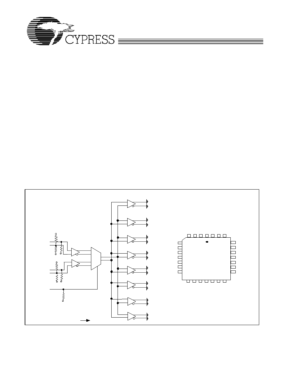
The CY2PP318 is a low-skew, low propagation delay 1-to-8
differential fanout buffer targeted to meet the requirements of
high-performance clock and data distribution applications. The
device is implemented on SiGe technology and has a fully
differential internal architecture that is optimized to achieve
low signal skews at operating frequencies of up to 1.5 GHz.
The device features two differential input paths that are multi-
plexed internally. This mux is controlled by the CLK_SEL pin.
The CY2PP318 may function not only as a differential clock
buffer but also as a signal-level translator and fanout on
ECL/PECL signal to eight ECL/PECL differential loads. An ex-
ternal bias pin, VBB, is provided for this purpose. In such an
application, the VBB pin should be connected to either one of
the CLKA# or CLKB# inputs and bypassed to ground via a
0.01-
µF capacitor.
Since the CY2PP318 introduces negligible jitter to the timing
budget, it is the ideal choice for distributing high frequency,
high precision clocks across back-planes and boards in
communication systems. Furthermore, advanced circuit
design schemes, such as internal temperature compensation,
ensure that the CY2PP318 delivers consistent performance
over various platforms.
Block Diagram
Pin Configuration
Q0
Q0#
Q1
Q1#
Q2
Q2#
Q3
Q3#
Q4
Q4#
Q5
Q5#
Q6
Q6#
Q7
Q7#
VBB
VEE
VEE
VCC
CLKA
CLKA#
CLKB
CLKB#
CLK_SEL
VEE
VCC
Q3
Q4
Q3#
VC
C
Q4#
Q5
Q5#
Q 0
Q 1
Q 0 #
V C C
Q 1 #
Q 2
Q 2 #
N C
C L K B #
Q 7 #
V C C
Q 7
Q 6 #
Q 6
VEE
CLKA
CL
K_
S
E
L
VC
C
C
LKA
#
VB
B
CL
KB
18
17
16
15
14
13
12
19
20
21
22
23
24
25
11
10
9
8
7
6
5
26
27
28
1
2
3
4
C Y 2 P P 3 1 8
T O P V IE W
FastEdgeTM Series
CY2PP318
Document #: 38-07501 Rev.*E
Page 2 of 8
Governing Agencies
The following agencies provide specifications that apply to the
CY2PP318. The agency name and relevant specification is
listed below in Table 2.
Pin Definitions
[1, 2, 3]
Pin
Name
I/O
Type
Description
3
VBB
O
Bias
Reference Voltage Output
26
VEE
PWR
Power
Negative Supply
1, 8, 15, 22
VCC
+PWR
Power
Positive Supply
28
CLKA
I, PD
ECL/PECL
ECL/PECL Differential Input Clocks
2
CLKA#
I, PD/PU ECL/PECL
ECL/PECL Differential Input Clocks
4
CLKB
I, PD
ECL/PECL
ECL/PECL Differential Input Clocks
5
CLKB#
I, PD/PU ECL/PECL
ECL/PECL Differential Input Clocks
27
CLK_SEL I, PD
ECL/PECL
ECL/PECL Input Clock Select
6
NC
No Connect
25,23,20,18,16,13,11,9
Q(0:7)
O
ECL/PECL
ECL/PECL Differential Output Clocks
24,21,19,17,14,12,10,7
Q(0;7)#
O
ECL/PECL
ECL/PECL Differential Output Clocks
Table 1.
Control
Operation
CLK_SEL
0
CLKA, CLKA# input pair is active (Default condition with no connection to pin)
CLKA can be driven with ECL- or PECL-compatible signals with respective power configurations
1
CLKB, CLKB# input pair is active.
CLKB can be driven with ECL- or PECL-compatible signals with respective power configurations
Table 2.
Agency Name
Specification
JEDEC
JESD 020B (MSL)
JESD 51 (Theta JA)
JESD 82 (ECL)
JESD 65B (skew,jitter)
Mil-Spec
883E Method 1012.1 (Thermal Theta JC)
Notes:
1. In the I/O column, the following notation is used: I for Input, O for Output, PD for Pull-Down, PU for Pull-Up, and PWR for Power
2. In ECL mode (negative power supply mode), V
EE
is either 3.3V or 2.5V and V
CC
is connected to GND (0V). In PECL mode (positive power supply mode), V
EE
is connected to GND (0V) and V
CC
is either +3.3V or +2.5V. In both modes, the input and output levels are referenced to the most positive supply (V
CC
) and are
between V
CC
and V
EE
.
3. V
BB
is available for use for single-ended bias mode for |3.3V| supplies (not |2.5V|).
FastEdgeTM Series
CY2PP318
Document #: 38-07501 Rev.*E
Page 3 of 8
Absolute Maximum Ratings
Parameter
Description
Condition
Min.
Max.
Unit
V
CC
Positive Supply Voltage
Non-Functional
0.3
4.6
V
V
EE
Negative Supply Voltage
Non-Functional
-4.6
0.3
V
T
S
Temperature, Storage
Non-Functional
65
+150
°C
T
J
Temperature, Junction
Non-Functional
150
°C
ESD
h
ESD Protection
Human Body Model
2000
V
M
SL
Moisture Sensitivity Level
3
N.A.
Gate Count Total Number of Used Gates
Assembled Die
28
gates
Multiple Supplies: The Voltage on any input or I/O pin cannot exceed the power pin during power-up. Power supply sequencing is NOT required.
Operating Conditions
Parameter
Description
Condition
Min.
Max.
Unit
I
BB
Output Reference Current
Relative to V
BB
|200|
uA
LU
I
Latch Up Immunity
Functional, typical
100
mA
T
A
Temperature, Operating Ambient
Functional
40
+85
°C
Ø
Jc
Dissipation, Junction to Case
Functional
39
[4]
°C/W
Ø
Ja
Dissipation, Junction to Ambient
Functional
60
[4]
°C/W
I
EE
Maximum Quiescent Supply Current
V
EE
pin
100
[5]
mA
C
IN
Input pin capacitance
3
pF
L
IN
Pin Inductance
1
nH
V
IN
Input Voltage
Relative to V
CC
[6]
0.3
V
CC
+ 0.3
V
V
TT
Output Termination Voltage
Relative to V
CC
[6]
V
CC
2
V
V
OUT
Output Voltage
Relative to V
CC
[6]
0.3
V
CC
+ 0.3
V
I
IN
Input Current
[7]
V
IN
= V
IL
, or V
IN
= V
IH
l150l
uA
PECL DC Electrical Specifications
Parameter
Description
Condition
Min.
Max.
Unit
V
CC
Operating Voltage
2.5V ± 5%, V
EE
= 0.0V
3.3V ± 5%, V
EE
= 0.0V
2.375
3.135
2.625
3.465
V
V
V
CMR
Differential Cross Point Voltage
[8]
Differential operation
1.2
V
CC
V
V
OH
Output High Voltage
I
OH
= 30 mA
[9]
V
CC
1.25
V
CC
0.7
V
V
OL
Output Low Voltage
V
CC
= 3.3V ± 5%
V
CC
= 2.5V ± 5%
I
OL
= 5 mA
[9]
V
CC
1.995
V
CC
1.995
V
CC
1.5
V
CC
1.3
V
V
V
IH
Input Voltage, High
Single-ended operation
V
CC
1.165
V
CC
0.880
[10]
V
V
IL
Input Voltage, Low
Single-ended operation
V
CC
1.945
[10]
V
CC
1.625
V
V
BB
[3]
Output Reference Voltage
Relative to V
CC
[6]
V
CC
1.620
V
CC
1.220
V
Notes:
4. Theta JA EIA JEDEC 51 test board conditions (typical value); Theta JC 883E Method 1012.1
5. Power Calculation: V
CC
* I
EE
+0.5 (I
OH
+ I
OL
) (V
OH
V
OL
) (number of differential outputs used); I
EE
does not include current going off chip.
6. where V
CC
is 3.3V±5% or 2.5V±5%
7. Inputs have internal pull-up/pull-down or biasing resistors which affect the input current.
8. Refer to Figure 1
9. Equivalent to a termination of 50
to VTT. I
OHMIN
=(V
OHMIN
-V
TT
)/50; I
OHMAX
=(V
OHMAX
-V
TT
)/50; I
OLMIN
=(V
OLMIN
-V
TT
)/50; I
OLMAX
=(V
OLMAX
-V
TT
)/50;
10. V
IL
will operate down to V
EE
; V
IH
will operate up to V
CC
FastEdgeTM Series
CY2PP318
Document #: 38-07501 Rev.*E
Page 4 of 8
ECL DC Electrical Specifications
Parameter
Description
Condition
Min.
Max.
Unit
V
EE
Negative Power Supply
2.5V ± 5%, V
CC
= 0.0V
3.3V ± 5%, V
CC
= 0.0V
2.625
3.465
2.375
3.135
V
V
CMR
Differential cross point voltage
[8]
Differential operation
V
EE
+ 1.2
0V
V
V
OH
Output High Voltage
I
OH
= 30 mA
[9]
1.25
0.7
V
V
OL
Output Low Voltage
V
EE
= 3.3V ± 5%
V
EE
= 2.5V ± 5%
I
OL
= 5 mA
[9]
1.995
1.995
1.5
1.3
V
V
IH
Input Voltage, High
Single-ended operation
1.165
0.880
[10]
V
V
IL
Input Voltage, Low
Single-ended operation
1.945
[10]
1.625
V
V
BB
[3]
Output Reference Voltage
1.620
1.220
V
AC Electrical Specifications
Parameter
Description
Condition
Min.
Max.
Unit
V
PP
Differential Input Voltage
[8]
Differential operation
0.1
1.3
V
F
CLK
Input Frequency
50% duty cycle Standard load
1.5
GHz
T
PD
Propagation Delay CLKA or CLKB to
Output pair
660 MHz
[11]
400
680
ps
Vo
Output Voltage (peak-to-peak; see Fig-
ure 2)
< 1 GHz
0.375
V
V
CMRO
Output Common Voltage Range (typ.)
V
CC
1.425
V
tsk
(0)
Output-to-output Skew
660 MHz
[11]
, See Figure 3
50
ps
tsk
(PP)
Part-to-Part Output Skew
660 MHz
[11]
150
ps
T
PER
Output Period Jitter (rms)
[12]
660 MHz
[11]
1.6
ps
tsk
(P)
Output Pulse Skew
[13]
660 MHz
[11]
, See Figure 3
35
ps
T
R
,T
F
Output Rise/Fall Time (see Figure 2)
660 MHz 50% duty cycle
Differential 20% to 80%
0.08
0.3
ns
Notes:
11. 50% duty cycle; standard load; differential operation
12. For 3.3V supplies. Jitter measured differentially using an Agilent 8133A Pulse Generator with an 8500A LeCroy Wavemaster Oscilloscope using at least 10,000
data points
13. Output pulse skew is the absolute difference of the propagation delay times: | t
PLH
t
PHL
|
FastEdgeTM Series
CY2PP318
Document #: 38-07501 Rev.*E
Page 5 of 8
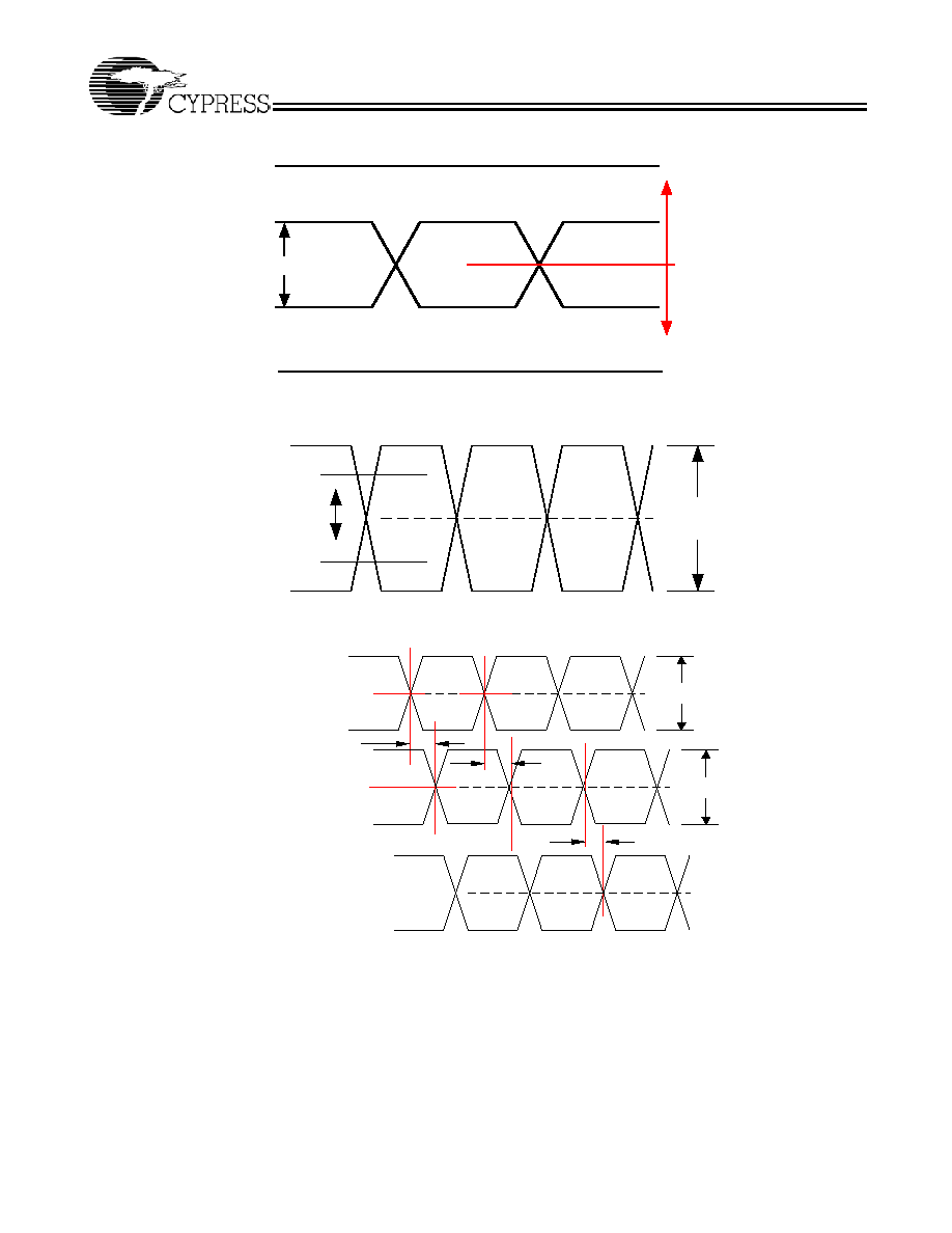
Timing Definitions
.
VIH
VIL
VCM R
VPP
VCMR Min = VEE + 1.2
VPP range
0.1V - 1.3V
VCMR Max = VCC
VCC
VEE
Figure 1. PECL/ECL Input Waveform Definitions
tr, tf,
20-80%
VO
Figure 2. ECL/LVPECL Output
Figure 3. Propagation Delay (T
PD
), output pulse skew (|t
PLH
-t
PHL
|), and output-to-output skew (t
SK(O)
)
for both CLKA or CLKB to Output Pair, PECL/ECL to PECL/ECL
V O
V P P
T P D
I n p u t
C l o c k
O u t p u t
C l o c k
A n o t h e r
O u t p u t
C l o c k
T P L H ,
T P H L
t S K ( O )
FastEdgeTM Series
CY2PP318
Document #: 38-07501 Rev.*E
Page 6 of 8
Test Configuration
Standard test load using a differential pulse generator and
differential measurement instrument.
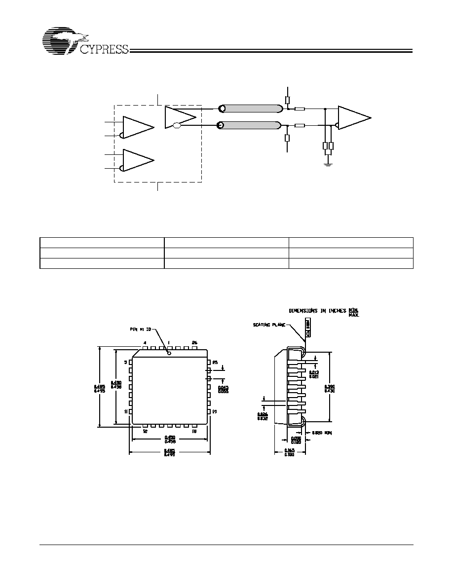
Applications Information
Termination Examples
P u ls e
G e n e ra to r
Z = 5 0 o h m
Z o = 5 0 o h m
V T T
V T T
R
T
= 5 0 o h m
Z o = 5 0 o h m
V T T
5 "
5 "
V T T
R
T
= 5 0 o h m
D U T
C Y 2 P P 3 1 8
R
T
= 5 0 o h m
R
T
= 5 0 o h m
Figure 4. CY2PP318 AC Test Reference
V T T
Z o = 5 0 o h m
V T T
5 "
5 "
C Y 2 P P 3 1 8
R
T
= 5 0 o h m
R
T
= 5 0 o h m
V C C
V E E
Figure 5. Standard LVPECL PECL Output Termination
V T T
Z o = 5 0 o h m
V T T
5 "
5 "
C Y 2 P P 3 1 8
R
T
= 5 0 o h m
R
T
= 5 0 o h m
V C C
V E E
V B B ( 3 . 3 V )
Figure 6. Driving a PECL/ECL Single-ended Input
FastEdgeTM Series
CY2PP318
Document #: 38-07501 Rev.*E
Page 7 of 8
© Cypress Semiconductor Corporation, 2004. The information contained herein is subject to change without notice. Cypress Semiconductor Corporation assumes no responsibility for the use
of any circuitry other than circuitry embodied in a Cypress product. Nor does it convey or imply any license under patent or other rights. Cypress products are not warranted nor intended to be
used for medical, life support, life saving, critical control or safety applications, unless pursuant to an express written agreement with Cypress. Furthermore, Cypress does not authorize its
products for use as critical components in life-support systems where a malfunction or failure may reasonably be expected to result in significant injury to the user. The inclusion of Cypress
products in life-support systems application implies that the manufacturer assumes all risk of such use and in doing so indemnifies Cypress against all charges.
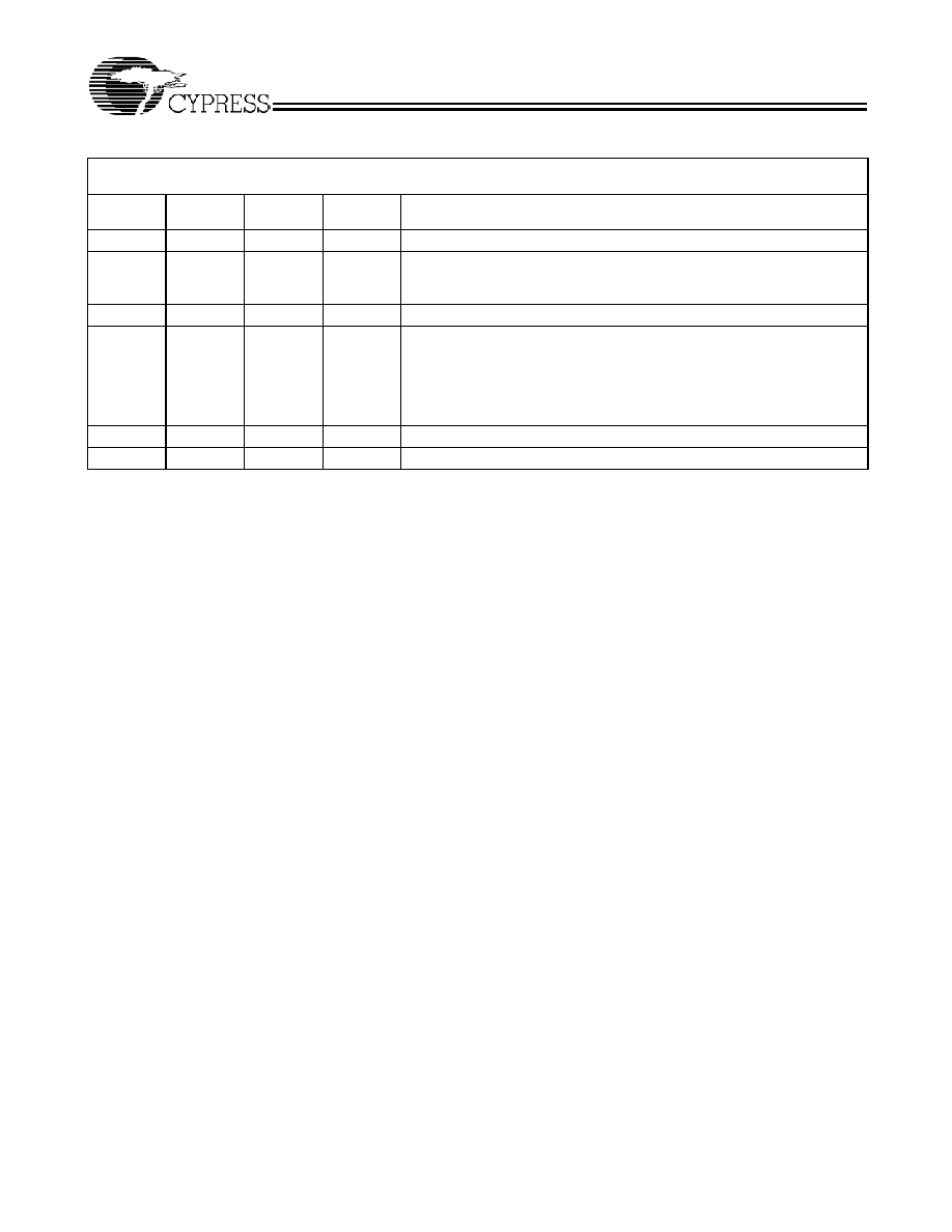
Package Drawing and Dimensions
FastEdge is a trademark of Cypress Semiconductor. All product and company names mentioned in this document are the
trademarks of their respective holders.
Ordering Information
Part Number
Package Type
Product Flow
CY2PP318JI
28-pin PLCC
Industrial, 40
° to 85°C
CY2PP318JIT
28-pin PLCC Tape and Reel
Industrial, 40
° to 85°C
3 . 3 V
Z o = 5 0 o h m
3 . 3 V
5 "
5 "
C Y 2 P P 3 1 8
1 2 0 o h m
1 2 0 o h m
V C C = 3 . 3 V
V E E = 0 V
L V D S
5 1 o h m
( 2 p la c e s )
3 3 o h m
( 2 p la c e s )
L V P E C L t o
L V D S
Figure 7. Low-voltage Positive Emitter-coupled Logic (LVPECL) to a Low-voltage Differential Signaling
(LVDS) Interface
28-lead Plastic Leaded Chip Carrier J64
51-85001-*A
FastEdgeTM Series
CY2PP318
Document #: 38-07501 Rev.*E
Page 8 of 8
Document History Page
Document Title: CY2PP318 FastEdgeTM Series 1 of 2:8 Differential Clock/Data Fanout Buffer
Document Number: 38-07501
REV.
ECN NO. Issue Date
Orig. of
Change
Description of Change
**
122041
02/13/03
RGL
New Data Sheet
*A
125923
06/11/03
RGL
Shifted the pin location
Changed the title (ComLink to FastEdge)
Corrected Specs that does not match EROS/IROS
*B
204240
See ECN
RGL
Change pin 1 from VCC to VCCO
*C
222602
See ECN
RGL
Changed the ECL and PECL mode ranges in the features section
Specified tsk max value to 150ps
Replaced I
CC
calculation with power calculation in the footnote.
Reformatted datasheet
Revised jitter spec as period jitter (rms)
Max operating frequency 1.5 GHz
*D
229352
See ECN
RGL
Added JEDEC Spec for MSL
*E
247624
See ECN
RGL/GGK Changed V
OH
and V
OL
to match with the Char Data