
High-performance SiS645/650 Pentium
4 Clock Synthesizer
CY28342
Cypress Semiconductor Corporation
·
3901 North First Street
·
San Jose
·
CA 95134
·
408-943-2600
Document #: 38-07349 Rev. *A
Revised July 29, 2002
42
Features
· Supports Pentium
4-type CPUs
· 3.3V power supply
· Eight copies of PCI clocks
· One 4-MHz USB clock
· Two copies of ZCLK clocks
· One 48-MHz/24-MHz programmable SIO clock
· Two differential CPU clock pairs
· SMBus support with read-back capabilities
· Spread Spectrum EMI reduction
· Dial-a-Frequency
®
features
· Dial-a-RatioTM features
· Dial-a-dB
®
features
· 48-pin SSOP and TSSOP packages
· Watchdog Function
Note:
1.
Pins marked with [*] have internal pull-up resistors. Pins marked with [**] have internal pull-down resistors.
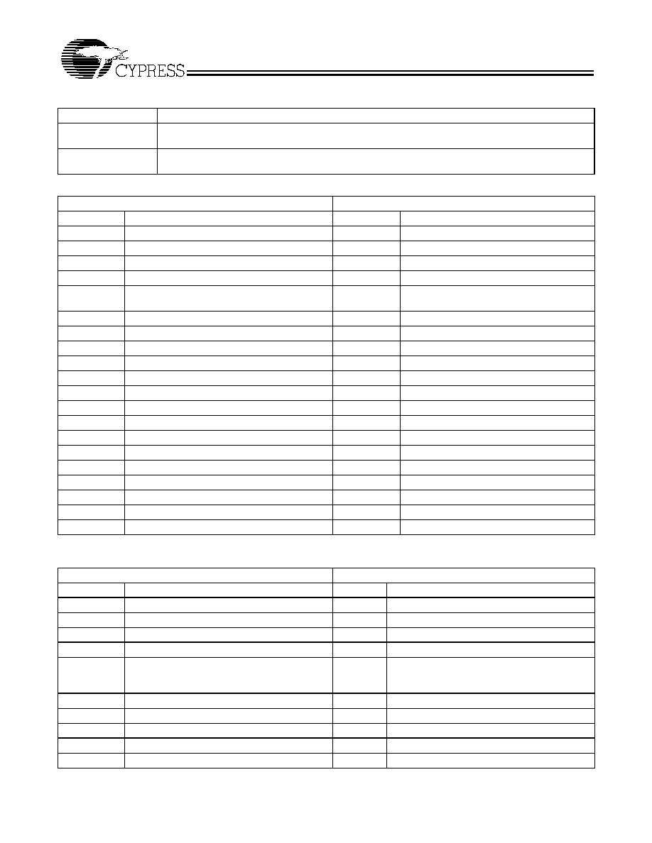
Block Diagram
Pin Configuration
[1]
PLL1
PLL2
/2
WD
Logic
XIN
XOUT
CPU_STP#
IREF
FS(0:4)
MULT0
VTTPWRGD
PCI_STP#
PD#
SDATA
SCLK
48M_24M#
48M
PCI_F(0:1)
PCI(0:5)
ZCLK(0:1)
AGP(0:1)
CPU(0:1)C
CPU(0:1)T
REF(0:2)
I2C
Logic
SRESET#
Power
on
Latch
SDCLK
1
2
3
4
5
6
7
8
9
10
11
12
13
14
15
16
17
18
19
20
21
22
23
24
48
47
46
45
44
43
42
41
40
39
38
37
36
35
34
33
32
31
30
29
28
27
26
25
VDDSD
SDCLK
VSSSD
CPU_STP#*
CPU1T
CPU1C
VDDC
VSSC
CPU0T
CPU0C
IREF
VSSA
VDDA
SCLK
SDATA
PD#/VTTPWRGD*
VSSAGP
AGP0
AGP1
VDDAGP
VDD48M
48M
24_48M/MULT0*
VSS48M
VDDR
**FS0/REF0
**FS1/REF1
**FS2/REF2
VSSR
XIN
XOUT
VSSZ
ZCLK0
ZCLK1
VDDZ
*SRESET#/PCI_STP#
VDDP
**FS3/PCI_F0
PCI0
**FS4/PCI_F1
PCI1
VSSP
VDDP
PCI2
PCI3
PCI4
PCI5
VSSP
&
<
48 Pin SSOP andf TSSOP

CY28342
Document #: 38-07349 Rev. *A
Page 2 of 22
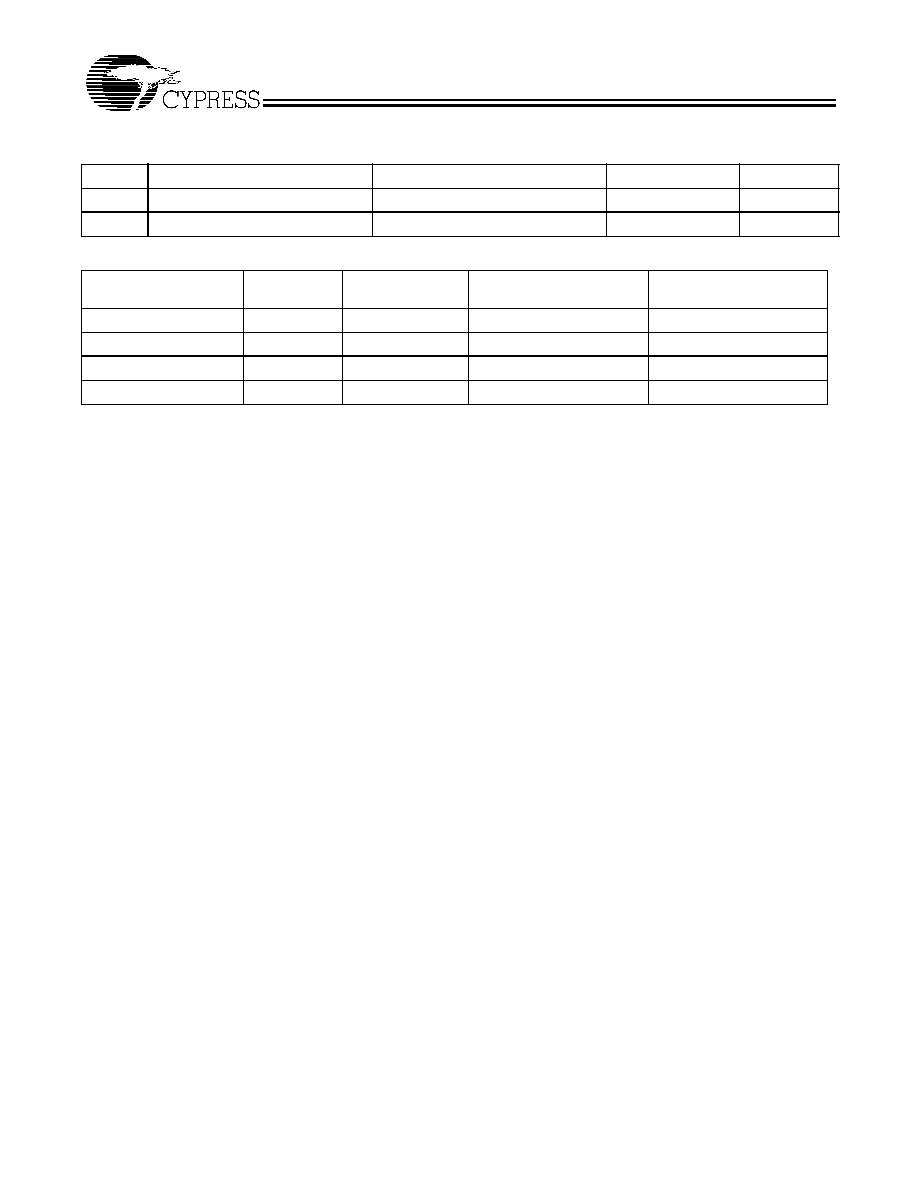
Table 1. Frequency Table
FS(4:0)
CPU (MHz)
SDRAM (MHz)
ZCLK (MHz)
AGP (MHz)
PCI (MHz)
VCO (MHz)
00000
100.20
100.20
66.80
66.80
33.40
400.8
00001
133.45
133.45
66.73
66.73
33.365
533.8
00010
100.20
133.60
66.80
66.80
33.40
400.8
00011
133.45
100.09
66.73
66.73
33.365
400.4
00100
100.20
167.00
62.63
62.63
31.315
501.0
00101
133.33
166.66
66.67
66.67
33.335
666.7
00110
100.20
150.30
66.80
66.80
33.40
601.2
00111
133.33
66.67
66.67
66.67
33.335
533.3
01000
100.20
120.24
66.80
66.80
33.40
601.2
01001
145.00
145.00
64.44
64.44
32.22
580.0
01010
111.11
133.33
66.67
66.67
33.335
666.7
01011
166.60
133.28
66.64
66.64
32.22
666.4
01100
66.80
66.80
66.80
66.80
33.40
400.8
01101
66.80
66.80
50.10
50.10
25.05
400.8
01110
100.20
133.60
100.20
66.80
33.40
400.8
01111
100.20
133.60
80.16
66.80
33.40
400.8
10000
100.20
167.00
83.50
62.63
31.315
501.0
10001
100.20
167.00
100.20
62.63
31.315
501.0
10010
102.20
136.27
68.13
68.13
34.065
408.8
10011
133.40
200.10
66.70
66.70
33.35
400.2
10100
105.00
140.00
70.00
70.00
35.00
420.0
10101
83.33
138.89
69.44
69.44
34.72
416.6
10110
108.00
144.00
72.00
72.00
36.00
432.0
10111
83.33
104.16
69.44
69.44
34.72
416.6
11000
116.00
145.00
64.44
64.44
32.22
580.0
11001
83.33
166.67
62.50
62.50
31.25
500.0
11010
120.00
150.00
66.67
66.67
33.335
600.0
11011
95.00
142.50
63.33
63.33
31.665
570.0
11100
112.00
140.00
62.22
62.22
31.11
560.0
11101
75.00
125.00
62.50
62.50
31.25
375.0
11110
108.00
180.00
67.50
67.50
33.75
540.0
11111
95.00
158.33
79.17
79.17
39.585
475.0

CY28342
Document #: 38-07349 Rev. *A
Page 3 of 22
Pin Description
[2]
Pin
Name
PWR
I/O
Description
6
XIN
I
Oscillator buffer input. Connect to a crystal or to an external clock.
7
XOUT
VDDR
O
Oscillator buffer output. Connect to a crystal. Do not connect when
an external clock is applied at XIN.
39,40,43,44
CPU (0:1)T,
CPU (0:1)C
VDDC
O
Differential host output clock pairs. See Table 1 for frequencies and
functionality.
16,17,20,23
PCI (0:5)
VDDP
O
PCI clock outputs. See Table 1.
14
FS3/PCI_F0
VDDP
I/O
PD
Power-on bidirectional Input/Output (I/O). At power-up, FS3 is the
input. When VTTPWRGD transitions to a logic HIGH, FS3 state is
latched and this pin becomes PCI_F0 clock output. See Table 1.
15
FS4/PCI_F1
VDDP
I/O
PD
Power-on bidirectional I/O. At power-up, FS4 is the input. When
VTTPWRGD transitions to a logic HIGH, FS4 state is latched and this
pin becomes PCI_F1 Clock Output. See Table 1.
2
FS0/REF0
VDDR
I/O
PD
Power-on bidirectional I/O. At power-up, FS0 is the input. When
VTTPWRGD transitions to a logic HIGH, FS0 state is latched and this
pin becomes REF0, buffered Output copy of the device's XIN clock.
3
FS1/REF1
VDDR
I/O
PD
Power-on bidirectional I/O. At power-up, FS1 is the input. When
VTTPWRGD is transited to logic LOW, FS1 state is latched and this pin
becomes REF1, buffered Output copy of the device's XIN clock.
4
FS2/REF2
VDDR
I/O
PD
Power-on bidirectional I/O. At power-up, FS2 is the input. When
VTTPWRGD is transited to logic LOW, FS2 state is latched and this pin
becomes REF2, buffered Output copy of the device's XIN clock.
38
IREF
I
Current reference programming input for CPU buffers. A resistor is
connected between this pin and V
SS
. See Figure 8.
33
PD#/VTTPR
GD
I
PU
Power-down input/VTT power good input. At power-up, VTTPWRGD
is the input. When this input is transitions initially from LOW to HIGH,
the FS (0:4) and MULT0 are latched. After the first LOW-to-HIGH
transition, this pin becomes a PD# input with an internal pull-up. When
PD# is asserted LOW, the device enters power-down mode. See power
management function.
27
48M
VDD48M
O
Fixed 48-MHz USB clock output.
26
24_48M/MUL
T0
VDD48M
I/O
PU
Power-on bidirectional I/O. At power-up, MULT0 is the input. When
VTTPWRGD is transitions to logic HIGH MULT0 state is latched and this
pin becomes 24_48M, SIO programmable clock output.
9,10
ZCLK (0:1)
VDDZ
O
HyperZip Clock Outputs. See Table 1.
34
SDATA
I/O
Serial Data Input. Conforms to the SMBus specification of a Slave
Receive/Transmit device. It is an input when receiving data, and an open
drain output when acknowledging or transmitting data.
35
SCLK
I
Serial Clock Input. Conforms to the SMBus specification.
12
SRESET#
O
PCI Clock Disable Input. If Byte12 Bit7 = 0, this pin becomes an
SRESET# open drain output, and the internal pull-up is not active. See
system reset description.
PCI_STP#
I
PU
System Reset Control Output. If Byte12 Bit7 = 1 (Default), this pin
becomes PCI Clock Disable Input. When PCI_STP# is asserted LOW,
PCI (0:5) clocks are synchronously disabled in a LOW state. This pin
does not affect PCI_F (0:1) if they are programmed to be free-running
clocks via the device's SMBus interface.
45
CPU_STP#
I
PU
CPU Clock Disable Input. When asserted LOW, CPU (0:1)T clocks are
synchronously disabled in a HIGH state and CPU (0:1)C clocks are
synchronously disabled in a LOW state.

CY28342
Document #: 38-07349 Rev. *A
Page 4 of 22
Serial Data Interface
To enhance the flexibility and function of the clock synthesizer,
a two-signal serial interface is provided. Through the Serial
Data Interface (SDI), various device functions such as
individual clock output buffers, etc., can be individually
enabled or disabled.
The registers associated with the SDI initializes to their default
setting upon power-up, and therefore the use of this interface
is optional. Clock device register changes are normally made
upon system initialization, if any are required. The interface
can also be used during system operation for power
management functions.
Data Protocol
The clock driver serial protocol accepts byte Write, byte Read,
block Write, and block Read operations from the controller. For
a block Write/Read operation, the bytes must be accessed in
sequential order from lowest to highest byte (most significant
bit first) with the ability to stop after any complete byte has
been transferred. For byte Write and byte Read operations,
the system controller can access individual indexed bytes. The
offset of the indexed byte is encoded in the command code,
as described in Table 2.
The block Write and block Read protocol is outlined in Table 3
while Table 4 outlines the corresponding byte Write and byte
Read protocol.
The slave receiver address is 11010010 (D2h).
Note:
2.
PU = Internal pull-up. PD = internal pull-down. T = Tri-level logic input with valid logic voltages of LOW = < 0.8V, T = 1.0 1.8V, and HIGH = > 2.0V.
47
SDCLK
VDDSD
O
SDRAM Clock Output.
30,31
AGP (0:1)
VDDAGP
O
AGP Clock Outputs. See Table 1 for frequencies and functionality.
48
VDDSD
PWR
3.3V power supply for SDRAM clock output.
29
VDDAGP
PWR
3.3V power supply for AGP clock output.
11
VDDZ
PWR
3.3V power supply for HyperZip clock output.
1
VDDR
PWR
3.3V power supply for REF clock output.
13,19
VDDP
PWR
3.3V power supply for PCI clock output.
42
VDDC
PWR
3.3V power supply for CPU clock output.
28
VDD48M
PWR
3.3V power supply for 48-MHz/24-MHz clock output.
36
VDDA
PWR
3.3V analog power supply.
18,24
VSSP
PWR
GND for PCI clocks outputs.
41
VSSC
PWR
GND for CPU clocks outputs.
8
VSSZ
PWR
GND for HyperZip clocks outputs.
25
VSS48M
PWR
GND for 48-MHz/24-MHz clocks outputs.
5
VSSR
PWR
GND for REF clocks outputs.
46
VSSSD
PWR
GND for SDRAM clocks outputs.
32
VSSAGP
PWR
GND for AGP clocks outputs.
37
VSSA
PWR
GND for analog.
Pin Description
(continued)
[2]
Pin
Name
PWR
I/O
Description
CY28342
Document #: 38-07349 Rev. *A
Page 5 of 22
Table 2. Command Code Definition
Bit
Description
7
0 = Block Read or block Write operation
1 = Byte Read or byte Write operation
(6:0)
Byte offset for byte Read or byte Write operations. For block Read or block Write operations, these bits
should be "0000000"
Table 3. Block Read and Block Write Protocol
Block Write Protocol
Block Read Protocol
Bit
Description
Bit
Description
1
Start
1
Start
2:8
Slave address 7 bits
2:8
Slave address 7 bits
9
Write
9
Write
10
Acknowledge from slave
10
Acknowledge from slave
11:18
Command code 8-bit "00000000" stands for
block operation
11:18
Command code 8-bit "00000000" stands for
block operation
19
Acknowledge from slave
19
Acknowledge from slave
20:27
Byte count 8 bits
20
Repeat start
28
Acknowledge from slave
21:27
Slave address 7 bits
29:36
Data byte 0 8 bits
28
Read
37
Acknowledge from slave
29
Acknowledge from slave
38:45
Data byte 1 8 bits
30:37
Byte count from slave 8 bits
46
Acknowledge from slave
38
Acknowledge
....
Data byte N/slave acknowledge...
39:46
Data byte from slave 8 bits
....
Data byte N 8 bits
47
Acknowledge
....
Acknowledge from slave
48:55
Data byte from slave 8 bits
....
Stop
56
Acknowledge
....
Data bytes from slave/acknowledge
....
Data byte N from slave 8 bits
....
Not acknowledge
....
Stop
Table 4. Byte Read and Byte Write Protocol
Byte Write Protocol
Byte Read Protocol
Bit
Description
Bit
Description
1
Start
1
Start
2:8
Slave address 7 bits
2:8
Slave address 7 bits
9
Write
9
Write
10
Acknowledge from slave
10
Acknowledge from slave
11:18
Command Code 8 bit "1xxxxxxx" stands for
byte operation bit[6:0] of the command code
represents the offset of the byte to be accessed
11:18
Command Code 8-bit "1xxxxxxx" stands for
byte operation bit[6:0] of the command code
represents the offset of the byte to be accessed
19
Acknowledge from slave
19
Acknowledge from slave
20:27
Byte count 8 bits
20
Repeat start
28
Acknowledge from slave
21:27
Slave address 7 bits
29
Stop
28
Read
29
Acknowledge from slave

CY28342
Document #: 38-07349 Rev. *A
Page 6 of 22
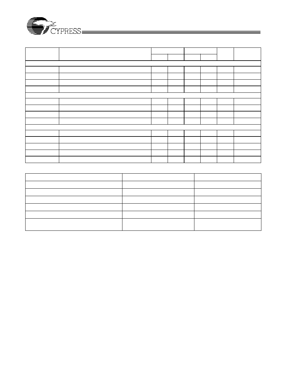
Since SDR and DDR Zero Delay Buffers will share this same address, the device starts from Byte 4.
30:37
Data byte from slave 8 bits
38
Not acknowledge
39
Stop
Byte 4: CPU Clock Register (All bits are Read and Write functional)
Bit
@Pup
Pin#
Name
Description
7
H/W Setting
14
FS3
For selecting frequencies in Table 1.
6
H/W Setting
4
FS2
For selecting frequencies in Table 1.
5
H/W Setting
3
FS1
For selecting frequencies in Table 1.
4
H/W Setting
2
FS0
For selecting frequencies in Table 1.
3
0
0 = HW, 1 = SW frequency selection.
2
H/W Setting
15
FS4
For selecting frequencies in Table 1.
1
1
SSCG
Spread Spectrum Enable. 0 = spread off, 1 = spread on.
This is a Read and Write control bit.
0
0
Master output control 0 = running, 1 = three-state all outputs.
Table 4. Byte Read and Byte Write Protocol (continued)
Byte Write Protocol
Byte Read Protocol
Bit
Description
Bit
Description
Byte 5: CPU Clock Register (all bits are Read-only)
Bit
@Pup
Pin#
Name
Description
7
0
Reserved.
6
0
Reserved.
5
X
26
MULT0
MULT0 (pin 26) value. This bit is Read-only.
4
X
15
FS4
FS4 Read-back. This bit is Read-only.
3
X
14
FS3
FS3 Read-back. This bit is Read-only.
2
X
4
FS2
FS2 Read-back. This bit is Read-only.
1
X
3
FS1
FS1 Read-back. This bit is Read-only.
0
X
2
FS0
FS0 Read-back. This bit is Read-only.
Byte 6: CPU Clock Register (All bits are Read and Write functional)
Bit
@Pup
Pin#
Name
Description
7
0
Function Test Bit. Always program to 0.
6
0
Reserved.
5
0
14
PCI_F0
PCI_STP# control of PCI_F0. 0 = free running, 1 = stopped when PCI_STP# is LOW.
4
0
15
PCI_F1
PCI_STP# control of PCI_F1. 0 = free running, 1 = stopped when PCI_STP# is LOW.
3
1
40,39
CPU0T/C
Controls CPU0T and CPU0C functionality when CPU_STP# is asserted LOW.
0 = free running, 1 = stopped with CPU_STP# asserted LOW.
This is a Read and Write control bit.
2
0
44,43
CPU1T/C
Controls CPU1T and CPU1C functionality when CPU_STP# is asserted LOW
0= Free Running, 1 Stopped with CPU_STP# asserted to LOW.
This and Read and Write control bit.
1
1
40,39
CPU0T/C
CPU0T, CPU0C output control, 1= enabled, 0 = disabled.
This is a Read and Write control bit.
0
1
44,43
CPU1T/C
CPU1T, CPU1C output control, 1= enabled, 0 = disabled.
This is a Read and Write control bit.

CY28342
Document #: 38-07349 Rev. *A
Page 7 of 22
Byte 7: PCI Clock Register (All bits are Read and Write functional)
Bit
@Pup
Pin#
Name
Description
7
1
15
PCI_F0
PCI_F0 output control 1 = enabled, 0 = forced LOW.
6
1
14
PCI_F1
PCI_F1 output control 1 = enabled, 0 = forced LOW.
5
1
23
PCI5
PCI5 output control 1 = enabled, 0 = forced LOW.
4
1
22
PCI4
PCI4 output control 1 = enabled, 0 = forced LOW.
3
1
21
PCI3
PCI3 output control 1 = enabled, 0 = forced LOW.
2
1
20
PCI2
PCI2 output control 1 = enabled, 0 = forced LOW.
1
1
17
PCI1
PCI1 output control 1 = enabled, 0 = forced LOW.
0
1
16
PCI0
PCI0 output control 1 = enabled, 0 = forced LOW.
Byte 8: Silicon Signature Register (all bits are Read-only)
Bit
@Pup
Description
7
1
Vendor ID
1000 = Cypress
6
0
5
0
4
0
3
0
Revision ID
2
0
1
0
0
0
Byte 9: Peripheral Control Register (All bits are Read and Write)
Bit
@Pup
Pin#
Name
Description
7
1
33
PD#
PD# Enable. 0 = enable, 1 = disable.
6
0
0 = when PD# asserted LOW, CPU(0:1)T stop in a high state, CPU(0:1)C stop in
a LOW state. 1 = when PD# asserted LOW, CPU(0:1)T and CPU(0:1)C stop in H-Z.
5
1
27
48M
48M output control 1 = enabled, 0 = forced LOW.
4
1
26
48M_24M
48M_24M output control 1 = enabled, 0 = forced LOW.
3
0
26
48M_24M
48M_24M, 0 = pin 26 output is 24MHz, 1= pin 28 output is 48 MHz.
2
0
SS2 Spread Spectrum control bit (0= down spread, 1= center spread).
1
0
SS1 Spread Spectrum control bit. See Table 9.
0
0
SS0 Spread Spectrum control bit. See Table 9.
Byte 10: Peripheral Control Register (All bits are Read and Write functional)
Bit
@Pup
Pin#
Name
Description
7
1
47
SDCLK
SDCLK output enable 1 = enabled, 0 = disabled.
6
1
4
REF2
REF2 output control 1 = enabled, 0 = forced LOW.
5
1
3
REF1
REF1 output control 1 = enabled, 0 = forced LOW.
4
1
2
REF0
REF0 output control 1 = enabled, 0 = forced LOW.
3
1
10
ZCLK1
ZCLK1 output enable 1 = enabled, 0 = disabled.
2
1
9
ZCLK0
ZCLK0 output enabled 1 = enabled, 0 = disabled.
1
1
30
AGP1
AGP1 output enabled 1 = enabled, 0 = disabled.
0
1
31
AGP0
AGP0 output enabled 1 = enabled, 0 = disabled.
CY28342
Document #: 38-07349 Rev. *A
Page 8 of 22
Byte 11: Dial-a-SkewTM and Dial-a-RatioTM Control Register (All bits are Read and Write functional)
Bit
@Pup
Name
Description
7
0
DARSD2 Programming these bits allows modifying the frequency ratio of the SDCLK clock relative to the VCO.
See Table 5.
6
0
DARSD1
5
0
DARSD0
4
0
DARAG2 Programming these bits allows modifying the frequency ratio of the AGP(1:0), PCI(5:0) and PCIF(0:1)
clocks relative to the VCO. See Table 6.
3
0
DARAG1
2
0
DARAG0
1
0
DASSD1 Programming these bits allows shifting skew between CPU and SDCLK signals. See Table 7.
0
0
DASSD0
Table 5. Dial-a-Ratio SDCLK
DARSD (2:0)
VC0/SDCLK ratio
000
Frequency selection default
001
2
010
3
011
4
100
5
101
6
110
8
111
9
Table 6. Dial-a-Ratio AGP(0:1)
[3]
DARAG (2:0)
VC0/AGP Ratio
000
Frequency selection default
001
6
010
7
011
8
100
9
101
10
110
10
111
10
Table 7. Dial-a-Skew SDCLK CPU
DASSD (1:0)
SDCLK-CPU Skew
00
0 ps (default)
[4]
01
+150 ps (CPU lag)*
10
+300 ps (CPU lag)*
11
+450 ps (CPU lag)*
Notes:
3.
The ratio of AGP to PCI is retained at 2:1.
4.
See Figure 8 for CPU measurement point. See
Figure 9 for SDCLK measurement point.

CY28342
Document #: 38-07349 Rev. *A
Page 9 of 22
Byte 12: Watchdog Time Stamp Register (All bits are Read and Write functional)
Bit
@Pup
Name
Description
7
1
SRESET#/PCI_STP#. 1 = pin 12 is the input pin as PCI_STP# signal. 0 = pin 12 is the output pin
as SRESET# signal.
6
0
Frequency Revert. This bit allows setting the Revert Frequency once the system is rebooted due
to Watchdog time-out only. 0 = selects frequency of existing H/W setting. 1 = selects frequency of
the second to last S/W setting (the software setting prior to the one that caused a system reboot).
5
0
WDTEST. For WD-Test, ALWAYS program to "0."
4
0
WD Alarm. This bit is set to "1" when the Watchdog times out. It is reset to "0" when the system
clears the WD time stamps (WD3:0).
3
0
WD3 These bits select the Watchdog Time Stamp Value. See Table 8.
2
0
WD2
1
0
WD1
0
0
WD0
Table 8. Watchdog Time Stamp Table
WD(3:0)
FUNCTION
0000
Off
0001
1 second
0010
2 seconds
0011
3 seconds
0100
4 seconds
0101
5 seconds
0110
6 seconds
0111
7 seconds
1000
8 seconds
1001
9 seconds
1010
10 seconds
1011
11 seconds
1100
12 seconds
1101
13 seconds
1110
14 seconds
1111
15 seconds
Byte 13: Dial-a-Frequency Control Register N (All bits are Read and Write functional)
[5]
Bit
@Pup
Description
7
0
Reserved.
6
0
N6, MSB
5
0
N5
4
0
N4
3
0
N3
2
0
N2
1
0
N3
0
0
N0, LSB
Note:
5.
Byte 13 and Byte 14 should be Write together in every case.
CY28342
Document #: 38-07349 Rev. *A
Page 10 of 22
Dial-a-Frequency Feature
SMBus Dial-a-Frequency feature is available in this device via
byte 13 and byte 14. P is a large-value, phase-locked loop
(PLL) constant that depends on the frequency selection
achieved through the hardware selectors FS(4:0). P value
may be determined from the following table.
Spread Spectrum Clock Generation (SSCG)
Spread Spectrum is a modulation technique used to minimize
electromagnetic interference (EMI) radiation generated by
repetitive digital signals. A clock presents the greatest EMI
energy at the center of the frequency it is generating. Spread
Spectrum distributes this energy over a specific and controlled
frequency bandwidth, thereby causing the average energy at
any one point in this band to decrease in value. This technique
is achieved by modulating the clock away from its resting
frequency by a certain percentage (which also determines the
amount of EMI reduction). In this device, Spread Spectrum is
enabled by setting specific register bits in the SMBus control
bytes. See the SMBus register section of this data sheet for
the exact bit and byte functionally. The following table is a
listing of the modes and percentages of Spread Spectrum
modulation that this device incorporates.
Byte 14: Dial-a-Frequency Control Register (All bits are Read and Write functional)
[5]
Bit
@Pup
Description
7
0
Reserved.
6
0
R5 MSB
5
0
R4
4
0
R3
3
0
R2
2
0
R1
1
0
R0, LSB
0
0
R and N Register Load Gate. 0 = gate closed (data is latched), 1= gate open (data is loading
from SMBus registers into R and N)#.
FS(4:0)
P
00000, 00001, 00010, 00111, 01001, 01011,
01110, 01111, 10010, 10100, 10110
95996900
00100, 00101, 10000, 10001, 10101, 10111,
11000, 11010, 11100, 11101, 11110, 11111
76797520
00110, 01000, 01010, 01100, 01101, 11001,
11011
63997933
00011, 10011
127995867
Table 9. Spread Spectrum
SS2
SS1
SS0
Spread Mode
Spread%
0
0
0
Down
0, 0.50
0
0
1
Down
+0.12, 0.62
0
1
0
Down
+0.25, 0.75
0
1
1
Down
+0.50, 1.00
1
0
0
Center
+0.25, 0.25
1
0
1
Center
+0.37, 0.37
1
1
0
Center
+0.50, 0.50
1
1
1
Center
+0.75, 0.75
CY28342
Document #: 38-07349 Rev. *A
Page 11 of 22
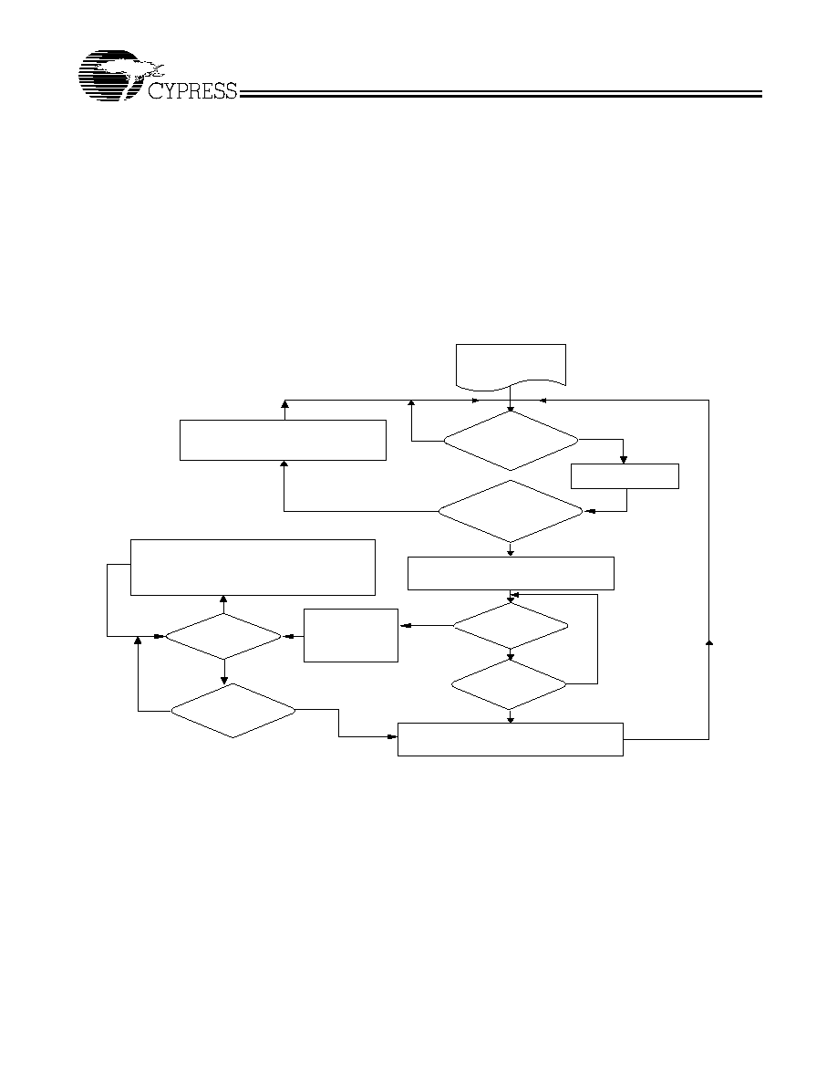
System Self-recovery Clock Management
This feature is designed to allow the system designer to
change frequency while the system is running and reboot the
operation of the system in case of a hang up due to the
frequency change.
When the system sends an SMBus command requesting
a frequency change through byte 4 or through bytes 13 and
14, it must have previously sent a command selecting which
time-out stamp the Watchdog must perform to byte 12, or the
system self-recovery feature will not be applicable. Conse-
quently this device will change frequency, and then the
Watchdog timer starts timing. Meanwhile, the system BIOS is
running its operation with the new frequency. If this device
receives a new SMBus command to clear the bits originally
programmed in byte 12, bits(3:0) (reprogram to 0000) before
Watchdog times out, this device will keep operating in its
normal condition with the new selected frequency. If the
Watchdog times out the first time before the new SMBus repro-
grams byte 12, bits(3:0) to (0000), then this device will send
a low system reset pulse, on SRESET# (see byte 12, bit 7),
and changes the Watchdog alarm (byte 12, bit 4) status to "1"
then restarts the Watchdog timer. If the Watchdog times out
a second time, this device will send another low pulse on
SRESET#, will relatch original hardware strapping frequency
(or second-to-last software-selected frequency, see byte 12,
bit6) selection, set Watchdog alarm bit (byte 12, bit4) to "1,"
then start the Watchdog timer again. The above-described
sequence will keep repeating until the BIOS clears the SMBus
byte 12 bits(3:0). Once the BIOS sets byte 12 bits(3:0) = 0000,
the Watchdog timer is turned off and the Watchdog alarm bit
(byte 12, bit 4) is reset to "0."
S y s t e m r u n n i n g w i t h
o r i g i n a l l y s e l e c t e d
f r e q u e n c y v i a
h a r d w a r e s t r a p p i n g .
R e c e i v e F r e q u e n c y
C h a n g e R e q u e s t v i a
S M B u s B y t e 4 o r V i a D i a l -
a - f r e q u e n c y ?
S t a r t i n t e r n a l w a t c h d o g t i m e r .
W a t c h D o g t i m e o u t ?
T u r n o f f w a t c h d o g t i m e r .
K e e p n e w f r e q u e n c y s e t t i n g . S e t W D a l a r m
b i t ( b y t e 1 2 , b i t 4 ) t o ''0 '
1 ) S e n d a n o t h e r 3 m S l o w p u l s e o n S R E S E T
2 ) R e l a t c h o r i g i n a l h a r d w a r e s t r a p p i n g s e l e c t i o n
f o r r e t u r n t o o r i g i n a l f r e q u e n c y s e t t i n g s .
3 ) S e t W D A l a r m b i t ( b y t e 1 2 , B i t 4 ) t o " 1 "
4 ) S t a r t W D t i m e r
F r e q u e n c y w i l l c h a n g e b u t S y s t e m S e l f
R e c o v e r y n o t a p p l i c a b l e ( n o t i m e s t a m p
s e l e c t e d a n d b y t e 1 2 , b i t ( 3 : 0 ) i s s t i l l =
" 0 0 0 0 "
N o
N o
Y e s
N o
N o
Y e s
S M B u s b y t e 1 2 t i m e
o u t s t a m p d i s a b l e d ?
I s S M B u s B y t e 9 , t i m e o u t
s t a m p e n a b l e d - ( b y t e 1 2 , b i t
( 3 : 0 ) 0 0 0 0 ) ?
C h a n g e t o a n e w
f r e q u e n c y
Y e s
1 ) S e n d S R E S E T
p u l s e
2 ) S e t W D b i t
( b y t e 1 2 , b i t 4 ) t o '1 '
3 ) S t a r t W D t i m e r
Y e s
W a t c h D o g t i m e o u t ?
N o
Y e s
S M B u s b y t e 9 t i m e o u t
s t a m p d i s a b l e d , B y t e
1 2 , b i t ( 3 : 0 ) = ( 0 0 0 0 ) ?
Y e s
N o
CY28342
Document #: 38-07349 Rev. *A
Page 12 of 22
Table 10. CPU Clock Current Select Function
Mult0
Board Target Trace/Term Z
Reference R, Iref V
DD
(3*Rr)
Output Current
Voh @ Z
0
50 Ohms (not used)
Rr = 221 1%, Iref = 5.00mA
I
OH
= 4*Iref
1.0V @ 50
1
50 Ohms
Rr = 475 1%, Iref = 2.32mA
I
OH
= 6*Iref
0.7V @ 50
Table 11. Group Timing Relationship and Tolerances
Offset
Tolerance
(or Range)
Conditions
Notes
CPU to SDCLK
Typical 0 ns
±2 ns
CPU leads
Note 6
CPU to AGP
Typical 2 ns
1-4ns
CPU leads
Note 6
CPU to ZCLK
Typical 2 ns
1-4ns
CPU leads
Note 6
CPU to PCI
Typical 2 ns
1-4ns
CPU leads
Note 6
Note:
6.
See Figure 8 for CPU clock-measurement point. See Figure 9 for SDCLK, AGP, ZCLK and PCI output-measurement points.
CY28342
Document #: 38-07349 Rev. *A
Page 13 of 22
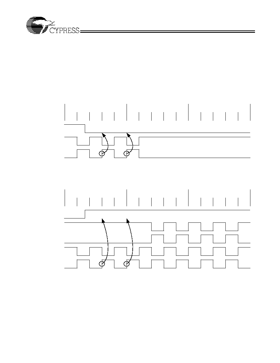
CPU_STP# Clarification
The CPU_STP# signal is an active LOW input used for
synchronous stopping and starting of the CPU output clocks
while the rest of the clock generator continues to function.
CPU_STP# Assertion
When CPU_STP# pin is asserted, all CPU outputs that are set
with the SMBus configuration to be stoppable via assertion of
CPU_STP# will be stopped after being sampled by two falling
CPU clock edges. The final state of the stopped CPU signals
is CPU = HIGH and CPU0# = LOW. There is no change to the
output drive current values during the stopped state. The CPU
is driven HIGH with a current value equal to (Mult0
"select") × (Iref), and the CPU# signal will not be driven. Due
to external pull-down circuitry, CPU# will be LOW during this
stopped state.
CPU_STP# Deassertion
The deassertion of the CPU_STP# signal will cause all CPU
outputs that were stopped to resume normal operation in a
synchronous manner. Synchronous manner meaning that no
short or stretched clock pulses will be produce when the clock
resumes. The maximum latency from the deassertion to active
outputs is no more than two CPU clock cycles.
CPU_STP#
CPUT
CPUC
Figure 1. Assertion CPU_STP# Waveform
CPU_STP#
CPUT
CPUC
CPUT
CPUC
Figure 2. Deassertion CPU_STP# Waveform

CY28342
Document #: 38-07349 Rev. *A
Page 14 of 22
PCI_STP# Assertion
The PCI_STP# signal is an active LOW input used for
synchronous stopping and starting the PCI outputs while the
rest of the clock generator continues to function. The set-up
time for capturing PCI_STP# going LOW is 10 ns (t
setup
). (See
Figure 3.) The PCI_F (0:2) clocks will not be affected by this
pin if their control bits in the SMBus register are set to allow
them to be free running.
PCI_STP# Deassertion
The deassertion of the PCI_STP# signal will cause all PCI(0:6)
and stoppable PCI_F(0:2) clocks to resume running in
a synchronous manner within two PCI clock periods after
PCI_STP# transitions to a high level.
Note:
7.
The PCI STOP function is controlled by 2 inputs. One is the device PCI_STP# pin number 34 and the other is SMBus byte 0 bit 3. These 2 inputs are logically
ANDed. If either the external pin or the internal SMBus register bit is set low then the stoppable PCI clocks will be stopped in a logic low state. Reading SMBus
Byte 0 Bit 3 will return a 0 value if either of these control bits are set LOW thereby indicating the device's stoppable PCI clocks are not running.
PCI_STP#
PCI_F(0:2) 33M
PCI(0:6) 33M
setup
t
Figure 3. Assertion PCI_STP# Waveform
PCI_STP#
PCI_F(0:2)
PCI(0:6)
setup
t
Figure 4. Deassertion PCI_STP# Waveform
[7]

CY28342
Document #: 38-07349 Rev. *A
Page 15 of 22
PD# (Power-Down) Clarification
The PD# (power-down) pin is used to shut off ALL clocks prior
to shutting off power to the device. PD# is an asynchronous
active LOW input. This signal is synchronized internally to the
device powering down the clock synthesizer. PD# is an
asynchronous function for powering up the system. When PD#
is low, all clocks are driven to a LOW value and held there and
the VCO and PLLs are also powered down. All clocks are shut
down in a synchronous manner so has not to cause glitches
while transitioning to the low "stopped" state.
PD# - Assertion (transition from logic "l" to logic "0")
When PD# is sampled LOW by two consecutive rising edges
of CPUC clock then all clock outputs (except CPUT) clocks
must be held LOW on their next HIGH-to-LOW transition.
CPUT clocks must be hold with CPUT clock pin driven HIGH
with a value of 2x Iref and CPUC undriven.
Due to the state of the internal logic, stopping and holding the
REF clock outputs in the LOW state may require more than
one clock cycle to complete.
PD# Deassertion (transition from logic "0" to logic "1")
The power-up latency between PD# rising to a valid logic "1"
level and the starting of all clocks is less than 3.0 ms.
Note:
8.
Device is not affected; VTTPWRGD is ignored.
P D #
C PU (0:1)T
C PU (0:1)C
C PU Internal
C PU # Internal
Figure 5. Power-down Assertion/Deassertion Timing Waveforms Nonbuffered Mode
VID (0:3),
SEL (0,1)
VTTPWRGD
PWRGD
VDD Clock Gen
Clock State
Clock Outputs
Clock VCO
0.2-0.3mS
Delay
State 0
State 2
State 3
Wait for
VTT_GD#
Sample Sels
Off
Off
On
On
State 1
(Note A)
Figure 6. VTTPWRGD Timing Diagram
[8]

CY28342
Document #: 38-07349 Rev. *A
Page 16 of 22
V
T
T
P
W
R
G
D
=
H
ig
h
D e la y 0 .2 5 m S
S 1
P o w e r O ff
S 0
V D D A = 2 .0 V
S a m p le
In p u ts
F S (3 :0 )
S 2
V D D 3 .3 = O ff
N o rm a l
O p e ra tio n
S 3
W a it fo r
1 .1 4 6 m s
E n a b le
O u tp u te s
Outputs
Figure 7. Clock Generator Power-up/Run State Diagram

CY28342
Document #: 38-07349 Rev. *A
Page 17 of 22
Maximum Ratings
Input Voltage Relative to V
SS
................................V
SS
0.3V
Input Voltage Relative to V
DDQ
or AV
DD
: ............. V
DD
+ 0.3V
Storage Temperature:................................. 65
°
C to +150
°
C
Operating Temperature: ................................... 0
°
C to +70
°
C
Maximum Power Supply:................................................ 3.5V
DC Characteristics
Current Accuracy
[9]
Conditions
Configuration
Load
Min.
Max.
Iout
V
DD
= nominal (3.30V)
M0= 0 or 1 and Rr shown in table
Nominal test
load for given
configuration
7% Inom
+7% Inom
Iout
V
DD
= 3.30 ±5%
All combinations of M0 or 1 and Rr
shown in table
Nominal test
load for given
configuration
12% Inom
+12% Inom
DC Component Parameters (V
DD
=3.3V±5%, TA = 0°C to 70°C)
Parameter
Description
Min.
Typ.
Max.
Units
Conditions
Idd3.3V
Dynamic Supply Current
280
mA
All frequencies at maximum values
[10]
Ipd3.3V
Power-down Supply Current
Note 11
mA
PD# Asserted
Cin
Input Pin Capacitance
5
pF
Cout
Output Pin Capacitance
6
pF
Lpin
Pin Inductance
7
nH
Cxtal
Crystal Pin Capacitance
30
36
42
pF
Measured from the X
IN
or X
OUT
Pin to
Ground
AC Parameters
Parameter
Description
100 MHz
133 MHz
Unit
Notes
Min.
Max.
Min.
Max.
Crystal
TDC
X
IN
Duty Cycle
47.5
52.5
47.5
52.5
%
12,13
TPeriod
X
IN
period
69.841
71.0
69.841
71.0
ns
12,13,14,15
VHIGH
X
IN
HIGH Voltage
0.7V
DD
V
DD
0.7V
DD
V
DD
V
VLOW
X
IN
LOW Voltage
0
0.3V
DD
0
0.3V
DD
V
Tr/Tf
X
IN
Rise and Fall Times
10.0
10.0
ns
TCCJ
X
IN
Cycle to Cycle Jitter
500
500
ps
13,14,16
CPU at 0.7V Timing
TSKEW
Any CPU to CPU Clock Skew
150
150
ps
16, 17, 18
TCCJ
CPU Cycle to Cycle Jitter
150
150
ps
16, 17, 18
TDC
CPU and CPUC Duty Cycle
45
55
45
55
%
16, 17, 18
TPeriod
CPU and CPUC Period
9.8
10.2
7.35
7.65
ns
16, 17, 18
Notes:
9.
Inom refers to the expected current based on the configuration of the device.
10. All outputs loaded as per maximum capacitive load table.
11.
Absolute value = (programmed CPU Iref 97) +10 mA.
12. This parameter is measured as an average over 1
-µ
s duration with a crystal center frequency of 14.318 MHz.
13. When X
IN
is driven from an external clock source.
14. All outputs loaded per Table 12 below.
15. Probes are placed on pins and measurements are acquired at 1.5V for 3.3V signals (see test and measurement set-up section).
16. This measurement is applicable with Spread ON or Spread OFF.
17. Measured at crossing point (Vx), or where subtraction of CLKCLK# crosses 0V.
18. For CPU load. See Figure 8.
CY28342
Document #: 38-07349 Rev. *A
Page 18 of 22
Tr/Tf
CPU and CPUC Rise and Fall Times
175
700
175
700
ps
16,19
Rise/Fall Matching
20%
20%
18,19,20
DeltaTr
Rise Time Variation
125
125
ps
18,19
DeltaTf
Fall Time Variation
125
125
ps
18,19
Vcross
Crossing Point Voltage at 0.7V Swing
280
430
280
430
mV
17,18,19
AGP
TDC
AGP Duty Cycle
45
55
45
55
%
14, 15
TPeriod
AGP Period
15.0
15.3
15.0
15.3
ns
14, 15
THIGH
AGP HIGH Time
5.25
5.25
ns
21
TLOW
AGP LOW Time
5.05
5.05
ns
22
Tr/Tf
AGP Rise and Fall Times
0.5
1.6
0.5
1.6
ns
14, 23
Tskew
Unbuffered
Any AGP to Any AGP Clock Skew
175
175
ps
14, 15
TCCJ
AGP Cycle-to-Cycle Jitter
250
250
ps
14, 15
ZCLK
TDC
ZCLK(0:1) Duty Cycle
45
55
45
55
%
14, 15
Tr/Tf
ZCLK(0:1) Rise and Fall Times
0.5
1.6
0.5
1.6
ns
14, 23
TSKEW
Any ZCLK(0:1) to Any ZCLK(0:1) Skew
175
175
ps
14, 15
TCCJ
ZCLK(0:1) Cycle-to-Cycle Jitter
250
250
ps
14,15
PCI
TDC
PCI_F(0:1) PCI (0:5) Duty Cycle
45
55
45
55
%
14, 15
TPeriod
PCI_F(0:1) PCI (0:5) Period
30.0
30.0
nS
12,14,15
THIGH
PCI_F(0:1) PCI (0:5) HIGH Time
12.0
12.0
nS
21
TLOW
PCI_F(0:1) PCI (0:5) LOW Time
12.0
12.0
nS
22
Tr/Tf
PCI_F(0:1) PCI (0:5) Rise and Fall times
0.5
2.0
0.5
2.0
nS
14, 23
TSKEW
Any PCI Clock to Any PCI Clock Skew
500
500
ps
14, 15
TCCJ
PCI_F(0:1) PCI (0:5) Cycle-to-Cycle Jitter
250
250
ps
14, 15
SDCLK
TDC
SDCLK Duty Cycle
45
55
45
55
%
14, 15
TPeriod
SDCLK Period
9.8
10.2
7.35
7.65
ns
14, 15
THIGH
SDCLK HIGH Time
3.0
1.87
ns
21
TLOW
SDCLK LOW Time
2.8
1.67
ns
22
Tr/Tf
SDCLK Rise and Fall Times
0.4
1.6
0.4
1.6
ns
14, 23
TCCJ
SDCLK Cycle-to-Cycle Jitter
250
250
ps
14, 23
48M
TDC
48M Duty Cycle
45
55
45
55
%
14, 15
TPeriod
48M Period
20.829 20.834 20.829 20.834
ns
14, 15
Tr/Tf
48M Rise and Fall Times
1.0
2.0
1.0
2.0
ns
14, 23
TCCJ
48M Cycle-to-Cycle Jitter
350
350
ps
14, 15
Notes:
19. Measured from V
OL
= 0.175 to V
OH
= 0.525V.
20. Determined as a fraction of 2*(TriseTfall)/(Trise+Tfall).
21. THIGH is measured at 2.4V for all non-host outputs.
22. TLOW is measured at 0.4V for all non-host outputs.
23. Probes are placed on pins and measurements are acquired between 0.4V and 2.4V for 3.3V signals (see test and measurement set-up section).
AC Parameters
(continued)
Parameter
Description
100 MHz
133 MHz
Unit
Notes
Min.
Max.
Min.
Max.
CY28342
Document #: 38-07349 Rev. *A
Page 19 of 22
24M
TDC
24-MHz Duty Cycle
45
55
45
55
%
14, 15
TPeriod
24-MHz Period
41.66
41.67
41.66
41.67
ns
14, 15
Tr/Tf
24-MHz Rise and Fall Times
1.0
4.0
1.0
4.0
ns
14, 23
TCCJ
24-MHz Cycle-to-Cycle Jitter
500
500
ps
14, 15
REF
TDC
REF Duty Cycle
45
55
45
55
%
14, 15
TPeriod
REF Period
69.8413
71.0
69.8413
71.0
ns
14, 15
Tr/Tf
REF Rise and Fall Times
1.0
4.0
1.0
4.0
ns
14, 23
TCCJ
REF Cycle-to-Cycle Jitter
1000
1000
ps
14, 15
ENABLE/DISABLE and SET UP
tpZL, tpZH
Output Enable Delay (All Outputs)
1.0
10.0
1.0
10.0
ns
tpLZ, tpZH
Output Disable Delay (All Outputs)
1.0
10.0
1.0
10.0
ns
tstable
All Clock Stabilization from Power-up
1.5
1.5
ms
tss
Stopclock Set-up Time
10.0
10.0
ns
tsh
Stopclock Hold Time
0
0
ns
24
AC Parameters
(continued)
Parameter
Description
100 MHz
133 MHz
Unit
Notes
Min.
Max.
Min.
Max.
Table 12. Maximum Lumped Capacitive Output Loads
Clock
Max. Load
Units
PCI(0:5), PCI_F(0:1)
30
pF
AGP (0:1), SDCLK
30
pF
ZCLK (0:1)
30
pF
48M_24, 48M Clock
20
pF
REF (0:2)
30
pF
CPU(0:1)T
CPU(0:1) C
2
pF
Notes:
24. CPU_STP# and PCI_STP# set-up time with respect to any PCI_F clock to guarantee that the affected clock will stop or start at the next PCI_F clock's rising
edge.
25. When crystal meets minimum 40 ohm device series resistance specification.
26. This is required for the duty cycle on the REF clock out to be as specified. The device will operate reliably with input duty cycles up to 30/70, but the REF
clock duty cycle will not be within data sheet specifications.
CY28342
Document #: 38-07349 Rev. *A
Page 20 of 22
Test and Measurement Set-up
For Differential CPU Output Signals
The following diagram shows lumped test load configurations
for the differential Host Clock Outputs.
CPUT
M ULTSEL
T
PCB
T
PCB
CPUC
33
33
49.9
49.9
M easurem ent Point
2 pF
475
IREF
M easurem ent Point
2 pF
Figure 8. 0.7V Configuration
2 .4 V
0 .4 V
3 .3 V
0 V
T r
T f
1 .5 V
3 .3 V s ig n a l s
tD C
P r o b e
O u tp u t u n d e r T e s t
L o a d C a p
-
-
Figure 9. Lumped Load For Single-Ended Output Signals (for AC Parameters Measurement)
Ordering Information
Part Number
Package Type
Product Flow
CY28342OC
48-pin Shrunk Small Outline Package (SSOP)
Commercial 0
°
to 70
°
C
CY28342OCT
48-pin Shrunk Small Outline Package (SSOP) Tape and Reel
Commercial 0
°
to 70
°
C
CY28342ZC
48-pin Thin Shrunk Small Outline Package (TSSOP)
Commercial 0
°
to 70
°
C
CY28342ZCT
48-pin Thin Shrunk Small Outline Package (TSSOP) Tape and Reel Commercial 0
°
to 70
°
C

CY28342
Document #: 38-07349 Rev. *A
Page 21 of 22
© Cypress Semiconductor Corporation, 2002. The information contained herein is subject to change without notice. Cypress Semiconductor Corporation assumes no responsibility for the use
of any circuitry other than circuitry embodied in a Cypress Semiconductor product. Nor does it convey or imply any license under patent or other rights. Cypress Semiconductor does not authorize
its products for use as critical components in life-support systems where a malfunction or failure may reasonably be expected to result in significant injury to the user. The inclusion of Cypress
Semiconductor products in life-support systems application implies that the manufacturer assumes all risk of such use and in doing so indemnifies Cypress Semiconductor against all charges.
Package Drawing and Dimensions
Pentium is a registered trademark of Intel Corporation. Dial-a-Frequency and Dial-a-dB are registered trademarks and Dial-a-Ratio
and Dial-a-Skew are trademarks of Cypress Semiconductor Corporation. All product and company names mentioned in this
document may be the trademarks of their respective holders.
48-lead Shrunk Small Outline Package O48
51-85061-*C
48-lead Thin Shrunk Small Outline Package, Type II (6 mm x 12 mm) Z48
51-85059-*B
CY28342
Document #: 38-07349 Rev. *A
Page 22 of 22
Document History Page
Document Title: CY28342 High-performance SiS645/650 Pentium
4 Clock Synthesizer
Document Number: 38-07349
REV.
ECN NO.
Issue Date
Orig. of
Change
Description of Change
**
111854
03/04/02
DMG
New Data Sheet
*A
117644
09/11/02
DMG
Changed the VTTPWRGD transition logic from LOW to HIGH in page 3.
Changed the Power Up default in Byte 9 Bit 3 from 1 to 0 in page 7.