18 Output, 3.3V SDRAM Buffer for
Desktop PCs with 4 DIMMs
CY2318ANZ
Cypress Semiconductor Corporation
·
3901 North First Street
·
San Jose
,
CA 95134
·
408-943-2600
Document #: 38-07181 Rev. *B
Revised January 19, 2005
Features
· One input to 18 output buffer/driver
· Supports up to four SDRAM DIMMs
· Two additional outputs for feedback
· Serial interface for individual output control
· 150ps typical output-output skew
· Up to 100 MHz operation
· Dedicated OE pin for testing
· Space-saving 48-pin SSOP package
· 3.3V operation
Functional Description
The CY2318ANZ is a 3.3V buffer designed to distribute
high-speed clocks in PC applications. The part has 18 outputs,
16 of which can be used to drive up to four SDRAM DIMMs,
and the remaining can be used for external feedback to a PLL.
The device operates at 3.3V and outputs can run up to 100
MHz, thus making it compatible with Pentium II
®
processors.
The CY2318ANZ can be used in conjunction with the CY2280,
CY2281, CY2282 or similar clock synthesizer for a complete
Pentium II motherboard solution.
The CY2318ANZ also includes a serial interface which can
enable or disable each output clock. On power-up, all output
clocks are enabled (internal pull up). A separate Output
Enable pin facilitates testing on ATE.
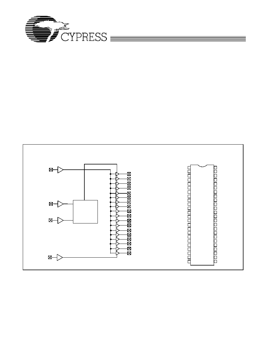
Block Diagram
Serial Interface
BUF_IN
SDATA
SCLOCK
SDRAM0
SDRAM1
SDRAM2
SDRAM3
SDRAM4
SDRAM5
SDRAM6
SDRAM7
1
2
3
4
NC
NC
V
DD
SDRAM15
SDRAM14
V
SS
V
DD
SDRAM13
SSOP
Top View
Pin Configuration
Decoding
8
5
6
7
12
9
10
11
13
14
15
16
20
17
18
19
24
21
22
23
48
47
46
45
41
44
43
42
37
40
39
38
36
35
34
33
29
32
31
30
25
28
27
26
SDRAM12
V
SS
OE
V
DD
SDRAM11
SDRAM10
V
SS
V
DD
SDRAM9
SDRAM8
V
SS
V
DD
SDRAM17
V
SS
V
SSIIC
SCLOCK
NC
NC
V
DD
SDRAM0
SDRAM1
V
SS
V
DD
SDRAM2
V
SS
BUF_IN
V
DD
SDRAM4
SDRAM5
V
SS
V
DD
SDRAM6
SDRAM7
V
SS
V
DD
SDRAM16
V
SS
V
DDIIC
SDATA
SDRAM3
SDRAM8
SDRAM9
SDRAM10
SDRAM11
SDRAM12
SDRAM13
SDRAM14
SDRAM15
SDRAM16
SDRAM17
OE

CY2318ANZ
Document #: 38-07181 Rev. *B
Page 2 of 9
Device Functionality
Pin Summary
Name
Pins
Description
V
DD
3, 7, 12, 16, 20, 29, 33, 37, 42, 46
3.3V Digital voltage supply
V
SS
6, 10, 15, 19, 22, 27, 30, 34, 39, 43 Ground
V
DDIIC
23
Serial interface voltage supply
V
SSIIC
26
Ground for serial interface
BUF_IN
11
Input clock (5V Tolerant)
OE
38
Output Enable (active HIGH), Three-state outputs when low
[1]
SDATA
24
Serial data input
[1]
SCLK
25
Serial clock input
[1]
SDRAM [03]
4, 5, 8, 9
SDRAM byte 0 clock outputs
SDRAM [47]
13, 14, 17, 18
SDRAM byte 1 clock outputs
SDRAM [811]
31, 32, 35, 36
SDRAM byte 2 clock outputs
SDRAM [1215] 40, 41, 44, 45
SDRAM byte 3 clock outputs
SDRAM [1617] 21, 28
SDRAM clock outputs usable for feedback
N/C
1, 2, 47, 48
Reserved for future modifications, do not connect in system
Note:
1. Internal pull-up resistor to V
DD
(value > 100 kohms)
OE
SDRAM [017]
0
Hi-Z
1
1 x BUF_IN

CY2318ANZ
Document #: 38-07181 Rev. *B
Page 3 of 9
Serial Configuration Map
· The Serial bits will be read by the clock driver in the following
order:
Byte 0 - Bits 7, 6, 5, 4, 3, 2, 1, 0
Byte 1 - Bits 7, 6, 5, 4, 3, 2, 1, 0
.
.
Byte N - Bits 7, 6, 5, 4, 3, 2, 1, 0
· Reserved and unused bits should be programmed to "0".
· Serial interface address for the CY2318ANZ is:
·
·
·
·
A6
A5
A4
A3
A2
A1
A0
R/W
1
1
0
1
0
0
1
----
Byte 0:SDRAM Active/Inactive Register
(1 = Active, 0 = Inactive), Default = Active
Bit
Pin #
Description
Bit 7 18
SDRAM7 (Active/Inactive)
Bit 6 17
SDRAM6 (Active/Inactive)
Bit 5 14
SDRAM5 (Active/Inactive)
Bit 4 13
SDRAM4 (Active/Inactive)
Bit 3 9
SDRAM3 (Active/Inactive)
Bit 2 8
SDRAM2 (Active/Inactive)
Bit 1 5
SDRAM1 (Active/Inactive)
Bit 0 4
SDRAM0 (Active/Inactive)
Byte 1: SDRAM Active/Inactive Register
(1 = Active, 0 = Inactive), Default = Active
Bit
Pin #
Description
Bit 7
45
SDRAM15 (Active/Inactive)
Bit 6
44
SDRAM14 (Active/Inactive)
Bit 5
41
SDRAM13 (Active/Inactive)
Bit 4
40
SDRAM12 (Active/Inactive)
Bit 3
36
SDRAM11 (Active/Inactive)
Bit 2
35
SDRAM10 (Active/Inactive)
Bit 1
32
SDRAM9 (Active/Inactive)
Bit 0
31
SDRAM8 (Active/Inactive)
Byte 2: SDRAM Active/Inactive Register
(1 = Active, 0 = Inactive), Default = Active
Bit
Pin #
Description
Bit 7
28
SDRAM17 (Active/Inactive)
Bit 6
21
SDRAM16 (Active/Inactive)
Bit 5
--
Reserved, drive to 0
Bit 4
--
Reserved, drive to 0
Bit 3
--
Reserved, drive to 0
Bit 2
--
Reserved, drive to 0
Bit 1
--
Reserved, drive to 0
Bit 0
--
Reserved, drive to 0

CY2318ANZ
Document #: 38-07181 Rev. *B
Page 4 of 9
Maximum Ratings
Supply Voltage to Ground Potential ..................0.5 to +7.0V
DC Input Voltage (except BUF_IN) .......... 0.5V to V
DD
+ 0.5
DC Input Voltage (BUF_IN).............................. 0.5V to 7.0V
Storage Temperature.................................. 65°C to +150°C
Junction Temperature ............................................... +150°C
Static Discharge Voltage............................................ >2000V
(per MIL-STD-883, Method 3015)
Operating Conditions
Parameter
Description
Min.
Max.
Unit
V
DD
, V
DDIIC
Supply Voltage
3.135
3.465
V
T
A
Operating Temperature (Ambient Temperature)
0
70
°C
C
L
Load Capacitance
20
30
pF
C
IN
Input Capacitance
7
pF
t
PU
Power-up time for all V
DD
s to reach minimum specified voltage
(power ramps must be monotonic)
0.05
50
ms
Electrical Characteristics
Over the Operating Range
Parameter
Description
Test Conditions
Min.
Max.
Unit
V
IL
Input LOW Voltage
[2]
For all pins except serial
interface pins
0.8
V
V
ILiic
Input LOW Voltage
For serial pins only
0.7
V
V
IH
Input HIGH Voltage
[2]
2.0
V
I
IL
Input LOW Current
(BUF_IN input)
V
IN
= 0V
10
10
µA
I
IL
Input LOW Current
(Except BUF_IN Pin)
V
IN
= 0V
100
µA
I
IH
Input HIGH Current
V
IN
= V
DD
10
10
µA
V
OL
Output LOW Voltage
[3]
I
OL
= 25 mA
0.4
V
V
OH
Output HIGH Voltage
[3]
I
OH
= 36 mA
2.4
V
I
DD
Supply Current
[3]
Unloaded outputs, 100 MHz
200
mA
I
DD
Supply Current
Loaded outputs, 100 MHz
360
mA
I
DD
Supply Current
[3]
Unloaded outputs, 66.67 MHz
150
mA
I
DD
Supply Current
Loaded outputs, 66.67 MHz
230
mA
I
DDS
Supply Current
BUF_IN = V
DD or
V
SS,
all other inputs at V
DD
500
µA
Notes:
2. BUF_IN input has a threshold voltage of V
DD
/2.
3. Parameter is guaranteed by design and characterization. Not 100% tested in production.

CY2318ANZ
Document #: 38-07181 Rev. *B
Page 5 of 9
Switching Characteristics
[4]
Parameter
Name
Test Conditions
Min.
Typ.
Max.
Unit
Maximum Operating Frequency
100
MHz
Duty Cycle
[3, 5]
= t
2
÷ t
1
Measured at 1.5V
45.0
50.0
55.0
%
t
3
Rising Edge Rate
[3]
Measured between 0.4V and 2.4V
0.9
1.5
4.0
V/ns
t
4
Falling Edge Rate
[3]
Measured between 2.4V and 0.4V
0.9
1.5
4.0
V/ns
t
5
Output to Output Skew
[3]
All outputs equally loaded
150
250
ps
t
6
SDRAM Buffer LH Prop. Delay
[3]
Input edge greater than 1 V/ns
1.0
3.5
5.0
ns
t
7
SDRAM Buffer HL Prop. Delay
[3]
Input edge greater than 1 V/ns
1.0
3.5
5.0
ns
t
8
SDRAM Buffer Enable Delay
[3]
Input edge greater than 1 V/ns
1.0
5
12
ns
t
9
SDRAM Buffer Disable Delay
[3]
Input edge greater than 1 V/ns
1.0
20
30
ns
Switching Waveforms
Notes:
4. All parameters specified with loaded outputs.
5. Duty cycle of input clock is 50%. Rising and falling edge rate is greater than 1 V/ns.
Duty Cycle Timing
t
1
t
2
1.5V
1.5V
1.5V
All Outputs Rise/Fall Time
OUTPUT
t
3
3.3V
0V
0.4V
2.4V
2.4V
0.4V
t
4
Output-Output Skew
1.5V
t
5
OUTPUT
OUTPUT
1.5V

CY2318ANZ
Document #: 38-07181 Rev. *B
Page 6 of 9
Switching Waveforms
(continued)
SDRAM Buffer LH and HL Propagation Delay
t
6
INPUT
OUTPUT
t
7
t
8
OE
OUTPUTS
SDRAM Buffer Enable and Disable Times
t
9
Three-State
Active
0.1
µF
V
DD
CLK out
C
LOAD
OUTPUTS
GND
Test Circuit

CY2318ANZ
Document #: 38-07181 Rev. *B
Page 7 of 9
Application Circuit
0.1
µF
0.1
µF
VDD
Vss
VDDIIC
VssIIC
BUF_IN
SDATA
SCLK
+3.3V
Ct
Rs
SDRAM[0:17]
SDRAM[0:17]
CY2318ANZ: 48-pin SSOP
Rs
CPUCLK
CY2280: 48-pin SSOP
Rs = Series termination resistor
Ct = Optional cap to reduce EMI
Ordering Information
Ordering Code
Package Type
Operating
Range
CY2318ANZPVC11
48-pin SSOP
Commercial
CY2318ANZPVC11T
48-pin SSOP - Tape and Reel
Commercial
Lead-free
CY2318ANZOXC11
48-pin SSOP
Commercial
CY2318ANZOXC11T
48-pin SSOP- Tape and Reel
Commercial

CY2318ANZ
Document #: 38-07181 Rev. *B
Page 8 of 9
© Cypress Semiconductor Corporation, 2005. The information contained herein is subject to change without notice. Cypress Semiconductor Corporation assumes no responsibility for the use
of any circuitry other than circuitry embodied in a Cypress product. Nor does it convey or imply any license under patent or other rights. Cypress products are not warranted nor intended to be
used for medical, life support, life saving, critical control or safety applications, unless pursuant to an express written agreement with Cypress. Furthermore, Cypress does not authorize its
products for use as critical components in life-support systems where a malfunction or failure may reasonably be expected to result in significant injury to the user. The inclusion of Cypress
products in life-support systems application implies that the manufacturer assumes all risk of such use and in doing so indemnifies Cypress against all charges.
Pentium II is a registered trademark of Intel Corporation. All products and company names mentioned in this document may be
the trademarks of their respective holders.
Package Diagram
48-Lead Shrunk Small Outline Package O48
51-85061-*C

CY2318ANZ
Document #: 38-07181 Rev. *B
Page 9 of 9
Document History Page
Document Title: CY2318ANZ 18 Output, 3.3V SDRAM Buffer for Desktop PCs with 4 DIMMs
Document Number: 38-07181
REV.
ECN NO.
Issue
Date
Orig. of
Change
Description of Change
**
111857
12/09/01
DSG
Change from Spec number: 38-00771 to 38-07181
*A
121833
12/14/02
RBI
Power up requirements added to Operating Conditions Information
*B
310577
See ECN
RGL
Added Tape and Reel option
Added Lead-free Devices