
10-output, 400-MHz LVPECL Zero Delay Buffer
CY23020-3
Cypress Semiconductor Corporation
·
3901 North First Street
·
San Jose
,
CA 95134
·
408-943-2600
Document #: 38-07473 Rev. *A
Revised June 5, 2003
Features
· 400-ps max Total Timing Budget
(TTB
) window
· 10 LVPECL outputs
· 1 LVPECL differential input
· Selectable output frequency range from 100 to 400 MHz
· Multiply by 2 option
· 15-ps RMS Cycle-Cycle Jitter
· Power-down mode
· Lock indicator
· 3.3V power supply
· Available in 48-pin QFN package
Overview
TheCY23020-3 is a high-performance 400-MHz LVPECL
Output phase-locked loop (PLL)-based zero delay buffer
(ZDB) designed for high- speed clock distribution applications.
The device features a guaranteed TTB window specifying all
occurrences of output clocks with respect to the input
reference clock across variations in voltage, temperature,
process, frequency, and ramp rate.
Additionally, the CY23020-3 can be used as a fan-out buffer
via the S[1:2] control pins. In this mode, the PLL is bypassed
and the reference clock is routed to the output buffers.
Block Diagram
Pin Configurations
CY23020-3
48
47
46
45
44
43
42
41
40
39
38
37
13
14
15
16
17
18
19
20
21
22
23
24
1
2
3
4
5
6
7
8
9
10
11
12
36
35
34
33
32
31
30
29
28
27
26
25
F
B
O
U
T
+
V
D
D
F
B
I
N
+
F
B
I
N
-
N
C
L
O
C
K
V
D
D
C
G
N
D
C
R
E
F
-
R
E
F
+
V
D
D
Q
9
+
Q
4
-
G
N
D
S
2
S
1
M
U
L
R
A
N
G
E
G
N
D
C
V
D
D
C
V
D
D
C
G
N
D
C
G
N
D
Q
5
-
FBOUT-
GND
Q1-
Q1+
VDD
Q2+
Q2-
GND
Q3-
Q3+
VDD
Q4+
Q9-
GND
Q8-
Q8+
VDD
Q7+
Q7-
GND
Q6-
Q6+
VDD
Q5+
Q1+
Q1-
Q3+
Q3-
Q2+
Q2-
Q4+
Q4-
Q5+
Q4-
Q6+
Q6-
Q7+
Q7-
Q8+
Q8-
Q9+
Q9-
FBOUT+
FBOUT-
PLL
Control
Logic
FBIN-
FBIN+
S1:2
RANGE
MUL
REF-
REF+
÷
1/
÷
2
÷
1
÷
2
LOCK

CY23020-3
Document #: 38-07473 Rev. *A
Page 2 of 9
Pin Definitions
[1]
Pin Name
Pin No.
Pin
Type
Pin Description
REF+
REF-
39
40
I
Reference Inputs. Output signals are synchronized to the crossing point of REF+ and REF
signals. In DC mode, the REF+/REF- inputs must be held at opposite logical states. For
optimal performance, the impedances seen by these two inputs must be equal.
FBIN+
FBIN-
46
45
I
Feedback Inputs. Input FBIN+/FBIN- must be fed by one of the outputs to ensure proper
functionality. If the trace between FBIN+/FBIN- and FBOUT+/FBOUT- is equal in length to
the traces between the outputs and the signal destinations, then the signals received at the
destinations will be synchronized to the clock signal at REF+/REF- inputs. In DC mode,
FBIN+/FBIN- inputs must be held at opposite logical states. For best performance, the
impedances seen by these two inputs must be equal.
FBOUT+
FBOUT-
48
1
O
Feedback Output. In order to complete the phase locked loop, similar polarity outputs must
be connected back to the FBIN+ and FBIN- pins. Any of the outputs may actually be used
as the feedback source.
Q1+, Q1-
4, 3
O
Differential Q1 Outputs. Refer to Tables 1,2, and 3 for configuration.
Q2+, Q2-
6, 7
O
Differential Q2 Outputs. Refer to Tables 1,2, and 3 for configuration.
Q3+, Q3-
10, 9
O
Differential Q3 Outputs. Refer to Tables 1,2, and 3 for configuration.
Q4 +, Q4-
12, 13
O
Differential Q4 Outputs. Refer to Tables 1,2, and 3 for configuration.
Q5+, Q5-
25, 24
O
Differential Q5 Outputs. Refer to Tables 1,2, and 3 for configuration.
Q6+, Q6-
27, 28
O
Differential Q6 Outputs. Refer to Tables 1,2, and 3 for configuration.
Q7+, Q7-
31, 30
O
Differential Q7 Outputs. Refer to Tables 1,2, and 3 for configuration.
Q8+, Q8-
33, 34
O
Differential Q8 Outputs. Refer to Tables 1,2, and 3 for configuration.
Q9+, Q9-
37, 36
O
Differential Q9 Outputs. Refer to Tables 1,2, and 3 for configuration.
RANGE
1
18
I
Frequency Range Selection Input. To determine the correct connection for this pin, refer
to Table 2. This should be a static input
LOCK
43
O
PLL Locked Output. When this output is HIGH, the PLL in the CY23020-3 is in steady state
operation mode (Locked). When this signal is LOW, the PLL is in the process of locking onto
the reference signal.
S1:2
16, 15
I
Output/PLL Enable Selection Bits. Refer to Table 1.
VDDC
20, 21, 42
P
Analog Power Connection. Connect to 3.3V.
GNDC
19, 22, 41
G
Analog Ground Connection. Connect to common system ground plane.
VDD
5, 11, 26, 32,
38, 47
P
Output Buffer Power Connections. Connect 3.3V
GND
2, 8, 14, 23,
29, 35
G
Ground Connections. Connect to common system ground plane.
MUL
[2]
17
I
Multiplication Factor Select. When set HIGH, the outputs will run at twice the speed of the
reference signal. This should be a static input.
NC
44
NC
Do Not Connect. This pin must be left floating. This pin is used by the factory for testing
purposes.
Table 1. Output Configuration
S1
S2
Outputs
PLL
0
0
Three-state
Shutdown
0
1
Reserved
1
0
Reference Input
Shutdown
1
1
PLL Output
Enabled
Notes:
1.
There are no power-up sequence requirements on the power supply pins of the CY23020-3.
2.
RANGE and MUL have a ~100k pull-down.

CY23020-3
Document #: 38-07473 Rev. *A
Page 3 of 9
How to Implement Zero Delay
Typically, ZDBs multiply (fan-out) single-clock signals quantity
while simultaneously reducing or mitigating the time delay
associated with passing the clock through a buffering device.
In many cases the output clock is adjusted, in phase, to occur
later or more often before the device's input clock to
compensate for a design's physical delay inadequacies. Most
commonly this is done using a simple PCB trace as a time
delay element. The longer the trace the earlier the output clock
edges occur with respect to the reference input clock edges.
In this way such effects as undesired transit time of a clock
signal across a PCB can be compensated for.
Inserting Other Devices in Feedback Path
Due to the fact that the device has an external feedback path
the user has a wide range of control over its output to input
skewing effect. One of these is to be able to synchronize the
outputs of an external clock that is resultant from any of the
output clocks. This implementation can be applied to any
device (ASIC, multiple output clock buffer/driver, etc.) which is
put into the feedback path.
Referring to Figure 1, if the traces between the ASIC/buffer
and the destination of the clock signal(s) (A) are equal in length
to the trace between the buffer and the FBIN pin (B), the
signals at the destination(s) device (C) will be driven high at
the same time the Reference clock provided to the ZDB goes
high. Synchronizing the other outputs of the ZDB to the outputs
from the ASIC/Buffer is more complex however, as any propa-
gation delay in the ASIC/Buffer must be accounted for.
There are constraints when inserting other devices. If the
devices contain PLLs or excessively long delay times they can
easily cause the overall clocking system to become unstable
as the components interact. For these designs it is advisable
to contact Cypress for applications support.
Table 2. Frequency Range Setting
RANGE
Output Frequency Range
0
100200 MHz
1
200400 MHz
Table 3. Frequency Multiplication Table
MUL
Output Frequency
0
= REF
1
= 2 * REF
Reference
Signal
Feedback
Input
ASIC/
Buffer
Zero
Delay
Buffer
A
B
C
Figure 1. Output Buffer in Feedback Path
Table 4. Absolute Maximum Ratings
[3]
Parameter
Description
Rating
Unit
V
DD
Voltage on any V
DD
pin with respect to GND
0.5 to +5.0
V
V
IN
Voltage on any input pin with respect to GND
0.5 to V
DD
+ 0.5
V
T
STG
Storage Temperature
65 to +150
°C
T
A
Operation Temperature (QFN)
40 to 85
°C
T
J
Junction Temperature
135
°C
Table 5. PECL DC Output Specification
[4]
Parameter
Description
Conditions
V
CC
= 3.135
V
CC
= 3.3
V
CC
= 3.465
Min.
Max.
Min.
Max.
Min.
Max.
V
OH
1.835
2.435
2
2.6
2.165
2.765
V
OL
1.135
1.735
1.3
1.9
1.465
2.065
V
OH
(rel to V
CC
)
1.3
0.7
1.3
0.7
1.3
0.7
V
OL
(rel to V
CC
)
2
1.4
2
1.4
2
1.4
These result in the following mid point values:
[4]
V
MID
((V
OH +
V
OL
)/2)
1.485
2.085
1.65
2.25
1.815
2.415
V
MID
Relative to V
CC
1.65
1.05
1.65
1.05
1.65
1.05
Notes:
3.
Stresses greater than those listed in this table may cause permanent damage to the device. These represent a stress rating only. Operation of the device at
these or any other conditions above those specified in the operating sections of this specification is not implied. Maximum conditions for extended periods may
affect reliability.
4.
The midpoint voltage is average value of a waveform. For differential signals the midpoint is assumed to be the same for both the true and complement since
the V
OH
and V
OL
of both the true and complement signals in general should be the same. V
MID
is not necessarily equal to the differential crossover voltage,
which may be skewed if there is differential time delays between the signals.

CY23020-3
Document #: 38-07473 Rev. *A
Page 4 of 9
Min.
Max.
Unit
I
PD
Power-down Current
70°C, V
DD
max
100
µ
A
I
IL
V
IN
= 0
10
µ
A
I
IH
V
IN
= V
DD
100
µ
A
Table 5. PECL DC Output Specification (continued)
[4]
Parameter
Description
Conditions
V
CC
= 3.135
V
CC
= 3.3
V
CC
= 3.465
Min.
Max.
Min.
Max.
Min.
Max.
Table 6. V
DDC
= 3.3V ±5%, V
DD
= 3.3V ±5% (See Test Set-ups, C
L
= 5 pF)
Parameter
Description
Condition
Min.
Typ. Max.
Unit
I
DD
Loaded, V
DD
max, Cold, 400 MHz,
all outputs switching
300
mA
C
IN
REF or FBIN ± Pin Capacitance
4
5
6
pF
C
L
[5]
Load Cap
5
pF
V
ISW
Single Ended Input Swing
0.5
1.25
V
V
IX
[6]
Input Crossover Voltage
(expressed relative to V
DD
)
V
DD
1.79
V
DD
0.96
S
I
Input Slew Rate
Measured from V
IX MEAS
+ 0.15 to
V
IX MEAS
0.15. (20 80% of a min
input swing sig.)
0.9
4
V/ns
V
OSW
Single Ended Output Swing
0.6
1.1
V
V
OX
[7]
Output Crossing Point
VO
MID
= (VH_
MEAS
VL_
MEAS
)/2
VO
MID
0.20
VO
MID
0.20
V
OX
[8]
Output Crossing Point (relative
to V
DD
)
VO
MID
= (VH_
MEAS
VL_
MEAS
)/2
V
DD
1.79
V
DD
0.96
Table 7. V
DDC
= 3.3V ±5%, V
DD
= 3.3V ±5% (See Test Set-ups, C
L
= 5 pF)
Parameter
Description
Condition
Min.
Typ. Max.
Unit
S
O
Output Rise/Fall Slew
Rate
Measured from V
IX MEAS
+ 0.15 to V
IX MEAS
0.15.
(2080% of a min input swing sig.)
0.9
2
V/ns
D
I
Input Duty Cycle
Input duty cycle
40
60
%
D
O
Output Duty Cycle
Differential crossing point
45
55
%
T
PDIO
REFin-FBin prop delay
External feedback REF, FB same frequency
50
200
ps
T
PDIOD
REFin-FBin prop delay
External feedback REF, FB same frequency x2
50
150
ps
T
PDO
FBout to any output prop
delay
325
100
ps
T
PDOB
Output-Output skew within a bank
150
ps
T
PDOB133
Output-Output skew @133 MHz
75
ps
T
TB
Total Timing Budget
400
ps
T
JCCPP
Cycle-Cycle Jitter (1000
cycles) p-p
REF and outputs, same frequency
100
ps
T
JCCRMS
RMS Cycle-Cycle Jitter
REF and outputs, same frequency
15
ps
Tjccop
Ref = x2
125
ps
Tjrms
Ref = x2
30
ps
Notes:
5.
Same as input. PECL is assumed to drive single point loads.
6.
This is the output DC mid-voltage range ± the crossover voltage tolerance. Refer Input Voltage is assumed to be derived from same supply as part. This is why
it is spec'd relative to V
DD
.
7.
Crossover is within ± 20% of the center of the minimum swing.
8.
Crossover is within ± 20% of the center of the minimum swing.
CY23020-3
Document #: 38-07473 Rev. *A
Page 5 of 9
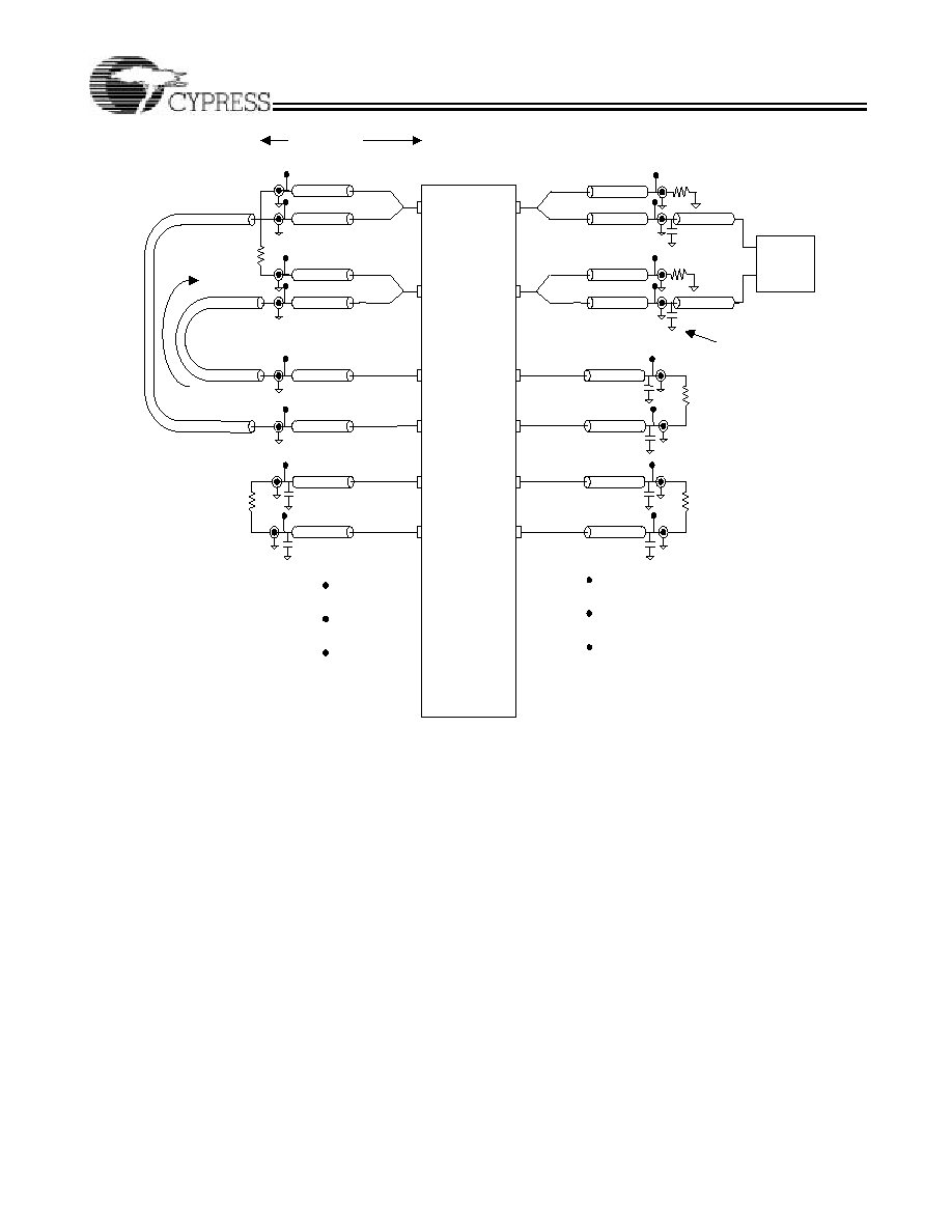
All board transmission lines 50
and 0.57 ns propagation delay
FBOUT+
2.3ns
FBOUT
-
Q1
+
Q5
+
Q5
-
C Selected to produce
1
-
2.5V/ns at pin
0.57 ns
Q1
-
C
L
Q
4+
Q
4
-
C
L
100
100
100
PULSE
GEN
FBIN
-
+
REF
-
=
REF+
FBIN+
100
FBIN+ OUT
50
REFIN+ OUT
50
REFIN
-
OUT
FBIN+ OUT
Figure 2. Test Set-up 1 Example