
DS-CPC5601-R3.0
www.clare.com
1
Features
·
Meets PC Card (PCMCIA) height requirements
·
Zero standby current
·
PCB real estate and cost savings
·
Can be used with LITELINK II and LITELINK III parts
Compliance
The supplied application circuits comply with the
requirements of TIA/EIA/IS-968 (FCC part 68),
UL1950, UL60950, EN60950, IEC60950, EN55022B,
CISPR22B, EN55024, and TBR-21.
Ordering Information
Figure 1. CPC5601 Block Diagram
Description
The CPC5601 is a serially-programmed driver IC for
use with Clare, Inc.
LITELINK Silicon Data Access
Arrangement (DAA) ICs
. The CPC5601 allows host-
equipment control of DAA characteristics for world-
wide DAA implementations, avoiding multiple imple-
mentations with discrete component changes or "stuff"
options. The small, low-profile package makes the
CPC5601 ideal for 56K PC Card (PCMCIA) modems,
PC motherboards, and soft-modems.
The CPC5601 uses opto-electronics to maintain the
isolation barrier required in the data access arrange-
ment for connection of host devices to the public
switched telephone network (PSTN).
The one-bit serial input of the CPC5601 recovers
clocking information from the input signal to set bits in
the shift register. The shift register outputs connect to
open-drain FET latches that are used to switch in dif-
ferent external components to set V/I slope, DC termi-
nation current limit, gain, and AC termination value in
LITELINK DAA implementations.The CPC5601 does
not need a clock signal for shift register operation, but
relies on internal timing instead.
The CPC5601 also includes an opto-coupler for ring
detection applications where the AC coupled ring
detector of the LITELINK DAA is not used.
Part Number
Description
CPC5601D
16-pin SOIC, .300 inch wide package
RING
GND
INPUT
NC
7
8
11
14
9
12
15
10
13
16
1
2
3
6
-BR
B6
B3
V
DDLINE
B5
B2
LED+
B4
B1
LED-
Shift
Register
Drivers
CPC5601 LITELINKTM Family
Auxiliary Programmable Driver IC

CPC5601
2
www.clare.com
R3.0
1 Specifications . . . . . . . . . . . . . . . . . . . . . . . . . . . . . . . . . . . . . . . . . . . . . . . . . . . . . . . . . . . . . . . . . . . . . . . . . . . . . . . . . . . . . . . . . . . . . . . 3
1. 1 Absolute Minimum and Maximum Ratings . . . . . . . . . . . . . . . . . . . . . . . . . . . . . . . . . . . . . . . . . . . . . . . . . . . . . . . . . . . . . . . . . . . . 3
1. 2 Electrical Characteristics. . . . . . . . . . . . . . . . . . . . . . . . . . . . . . . . . . . . . . . . . . . . . . . . . . . . . . . . . . . . . . . . . . . . . . . . . . . . . . . . . . 3
1. 3 Timing Characteristics . . . . . . . . . . . . . . . . . . . . . . . . . . . . . . . . . . . . . . . . . . . . . . . . . . . . . . . . . . . . . . . . . . . . . . . . . . . . . . . . . . . 4
1. 4 Pinout . . . . . . . . . . . . . . . . . . . . . . . . . . . . . . . . . . . . . . . . . . . . . . . . . . . . . . . . . . . . . . . . . . . . . . . . . . . . . . . . . . . . . . . . . . . . . . . . 4
1. 5 Mechanical Specifications. . . . . . . . . . . . . . . . . . . . . . . . . . . . . . . . . . . . . . . . . . . . . . . . . . . . . . . . . . . . . . . . . . . . . . . . . . . . . . . . . 5
2 Application . . . . . . . . . . . . . . . . . . . . . . . . . . . . . . . . . . . . . . . . . . . . . . . . . . . . . . . . . . . . . . . . . . . . . . . . . . . . . . . . . . . . . . . . . . . . . . . . . 6
2. 1 Application Circuit Configurations . . . . . . . . . . . . . . . . . . . . . . . . . . . . . . . . . . . . . . . . . . . . . . . . . . . . . . . . . . . . . . . . . . . . . . . . . . . 8
2. 2 AC Termination . . . . . . . . . . . . . . . . . . . . . . . . . . . . . . . . . . . . . . . . . . . . . . . . . . . . . . . . . . . . . . . . . . . . . . . . . . . . . . . . . . . . . . . . . 8
2. 3 LITELINK III Gain . . . . . . . . . . . . . . . . . . . . . . . . . . . . . . . . . . . . . . . . . . . . . . . . . . . . . . . . . . . . . . . . . . . . . . . . . . . . . . . . . . . . . . . 8
2. 4 Current Limiting. . . . . . . . . . . . . . . . . . . . . . . . . . . . . . . . . . . . . . . . . . . . . . . . . . . . . . . . . . . . . . . . . . . . . . . . . . . . . . . . . . . . . . . . . 8
2. 5 Figure 4 Part List. . . . . . . . . . . . . . . . . . . . . . . . . . . . . . . . . . . . . . . . . . . . . . . . . . . . . . . . . . . . . . . . . . . . . . . . . . . . . . . . . . . . . . . . 8
2. 6 Figure 5 Part List. . . . . . . . . . . . . . . . . . . . . . . . . . . . . . . . . . . . . . . . . . . . . . . . . . . . . . . . . . . . . . . . . . . . . . . . . . . . . . . . . . . . . . . 10
2. 7 Operational Sequence . . . . . . . . . . . . . . . . . . . . . . . . . . . . . . . . . . . . . . . . . . . . . . . . . . . . . . . . . . . . . . . . . . . . . . . . . . . . . . . . . . 11
2. 8 Output Current Ratings . . . . . . . . . . . . . . . . . . . . . . . . . . . . . . . . . . . . . . . . . . . . . . . . . . . . . . . . . . . . . . . . . . . . . . . . . . . . . . . . . . 11
3 Programming . . . . . . . . . . . . . . . . . . . . . . . . . . . . . . . . . . . . . . . . . . . . . . . . . . . . . . . . . . . . . . . . . . . . . . . . . . . . . . . . . . . . . . . . . . . . . . 12
3. 1 Latch Circuit Description . . . . . . . . . . . . . . . . . . . . . . . . . . . . . . . . . . . . . . . . . . . . . . . . . . . . . . . . . . . . . . . . . . . . . . . . . . . . . . . . . 12
3. 2 Programming Protocol . . . . . . . . . . . . . . . . . . . . . . . . . . . . . . . . . . . . . . . . . . . . . . . . . . . . . . . . . . . . . . . . . . . . . . . . . . . . . . . . . . 12
3. 3 Programming Example . . . . . . . . . . . . . . . . . . . . . . . . . . . . . . . . . . . . . . . . . . . . . . . . . . . . . . . . . . . . . . . . . . . . . . . . . . . . . . . . . . 13
4 Regulatory Information . . . . . . . . . . . . . . . . . . . . . . . . . . . . . . . . . . . . . . . . . . . . . . . . . . . . . . . . . . . . . . . . . . . . . . . . . . . . . . . . . . . . . . 13
5 LITELINK Design Resources . . . . . . . . . . . . . . . . . . . . . . . . . . . . . . . . . . . . . . . . . . . . . . . . . . . . . . . . . . . . . . . . . . . . . . . . . . . . . . . . . . 14
5. 1 Clare Design Resources . . . . . . . . . . . . . . . . . . . . . . . . . . . . . . . . . . . . . . . . . . . . . . . . . . . . . . . . . . . . . . . . . . . . . . . . . . . . . . . . . 14
5. 2 Third Party Design Resources . . . . . . . . . . . . . . . . . . . . . . . . . . . . . . . . . . . . . . . . . . . . . . . . . . . . . . . . . . . . . . . . . . . . . . . . . . . . 14

CPC5601
R3.0
www.clare.com
3
1. Specifications
1.1 Absolute Minimum and Maximum Ratings
1.2 Electrical Characteristics
Parameter
Minimum
Maximum
Unit
Conditions
Isolation Voltage
1500
-
V
RMS
From pins 1, 2, and 3 to
pins 7 through 16
Operating temperature
0
+85
°C
Storage temperature
-40
+125
°C
Soldering temperature
-
+220
°C
Parameter
Minimum
Typical
Maximum
Unit
Conditions
Data Input
Input high threshold current
-
1
5
mA
Input low threshold current
0.10
0.20
-
mA
Input voltage drop
0.9
1.2
1.4
V
I
F
= 5 mA
b1 Through b5 Output Driver
Output Current
-
-
10
mA
Output Breakdown Voltage
-
-
6
V
On Resistance
-
10
11
Supply voltage >= 2.8 V
b6 Output Driver
Output Current
-
-
120
mA
Output Breakdown Voltage
-
-
6
V
On Resistance
-
0.5
1.4
Supply voltage >= 2.8 V
Ring Detect Input
Input Control Current
6
20
100
mA
I
C
= 2 mA, V
CE
= 0.5 V
Input Voltage drop
0.9
1.2
1.4
V
I
F
= 5 mA
Ring Detect Output
Blocking Voltage
20
50
-
V
I
C
= 10 mA
Dark Current
-
50
500
nA
I
F
= 0 mA
Saturation Voltage
-
0.3
0.5
V
I
C
= 2 mA, I
F
= 16 mA
Current transfer ratio
33
400
-
%
I
F
= 6 mA, V
CE
= 0.5 V
Power Requirements
Supply Voltage
2.5
3.5
5.5
V
Total supply current (input current low)
-
0.01
1
µ
A
Total supply current (input current high)
-
10
20
µ
A
Specifications subject to change without notice. All performance characteristics based on the use of Clare, Inc. application circuits. Functional operation
of the device at conditions beyond those specified here is not implied. Specification conditions: V
DD
= 5V, temperature = 25 °C, unless otherwise indi-
cated.
Absolute maximum ratings are stress rat-
ings. Stresses in excess of these ratings
can cause permanent damage to the
device. Functional operation of the device
at these or any other conditions beyond
those indicated in the operational sections
of this data sheet is not implied. Exposure
of the device to the absolute maximum rat-
ings for an extended period may degrade
the device and affect its reliability.

CPC5601
4
www.clare.com
R3.0
1.3 Timing Characteristics
1.4 Pinout
Figure 2. CPC5601 Pinout
Parameter
Minimum
Typical
Maximum
Unit
Conditions
Setup time
50
-
-
µ
S
logic low before positive timing transi-
tion on input (pin 3)
Data hold time
60
-
-
µ
S
hold time after internal 140
µ
S
clock period
Data latch time
-
-
140
µ
S
from positive transition on input
Input hold time for output on
200
-
-
µ
S
Input hold time for output off
-
-
50
µ
S
Pin
Name
Function
1
RING
Opto-isolated ring output
2
GND
Analog host system ground
3
INPUT
Serial data input used to program outputs b1
through b6.
4
NC
No connection
5
NC
No connection
6
NC
No connection
7
BR-
Phone line side common
8
B6
Output b6
9
B5
Output b5
10 B4
Output b4
11 B3
Output b3
12 B2
Output b2
13 B1
Output b1
14 V
DDLINE
Telephone line side voltage source
15 LED+
Ring LED anode
16 LED-
Ring LED cathode
1
2
3
6
7
8
9
10
11
12
13
14
15
16

CPC5601
R3.0
www.clare.com
5
1.5 Mechanical Specifications
Figure 3. CPC5601 Mechanical Specifications
16-pin SOIC
1.981 ±.025
(.078 ±.001)
2.108 max
(.083)
1.106 typ.
(.040)
.635 x 45°
(.025 x 45°)
.254 ±.0127
(.010 ±.0005)
10.160 ±.051
(.400 ±.002)
10.363 ±.127
(.408 ±.005)
7.493 ±.127
(.295 ±.005)
1.270 typ.
(.050)
.406 typ.
(.016)
8.890 typ.
(.350)
1.270
(.050)
9.278 ±.051
(.383 ±.002)
1.193
(.047)
.787
(.031)
3.81 ±.381
(.150 ±.150)
.483 ±.102
(.019 ±.009)
Printed Circuit Board Pattern
(top view)
Dimensions:
mm
(inches)

CPC5601
6
www.clare.com
R3.0
2. Application
In the application circuits shown below, the CPC5601
is used to switch AC termination and gain. Loop-cur-
rent limit switching is optional.
Figure 4. CPC5601 Application Circuit Using the LITELINK II and the Optical Snoop Circuit
ąThis design was tested and found to comply with FCC part 68 with this part.
Other compliance requirements may require a different part.
˛Higher noise power supplies may require substitution of a 220
µ
H inductor,
Toko 380HB-2215 or similar. See the power quality section of Clare applica-
tion note AN-146,
Guidelines for Effective LITELINK Designs
for more informa-
tion. Both application circuits use the same components for setting AC
termination and the telephone line current limit.
3
Addition of this capacitor improves trans-hybrid loss.
R77 499K 1%
501K
0.015
301
REFM
C3 0.1
II

CPC5601
R3.0
www.clare.com
7
Figure 5. CPC5601 Application Circuit Using the LITELINK III and the LITELINK Snoop Circuit
ąThis design was tested and found to comply with FCC part 68 with this part.
Other compliance requirements may require a different part.
˛Higher noise power supplies may require substitution of a 220
µ
H inductor,
Toko 380HB-2215 or similar. See the power quality section of Clare applica-
tion note AN-146,
Guidelines for Effective LITELINK Designs
for more informa-
tion. Both application circuits use the same components for setting AC
termination and the telephone line current limit.
3
Addition of this capacitor improves trans-hybrid loss.
-BR
PROG
U4
CPC5601
1
2
3
4
5
6
7
8
16
15
14
13
12
11
10
9
RING
GND
PROG
NC
NC
NC
BR-
B6
LED-
LED+
VDDLINE
B1
B2
B3
B4
B5
C31
0.68 F
µ
C34
2.2 F
µ
R71
165
1%
R72
59
1%
-BR
-BR
R65
470
R73
R67 301 1%
R66 4.99K 1%
R76
100K
5%
1
2
+
-
OH
MODE
RING
CID
TX+
RX+
TX-
RX-
3.3 or 5 V
C13 0.1
C14 0.1
C2 0.1
C4 0.1
R1 (R
) 80.6K 1%
TX
R23˛
10
BR-
BR-
BR-
TIP
RING
1
2
3
4
5
6
7
8
9
10
11
12
13
14
15
16
32
31
30
29
28
27
26
25
24
23
22
21
20
19
18
17
VDD
TXSM
TX-
TX+
TX
GND
RX-
RX+
SNP+
SNP-
RXF
RX
MODE
OH
RING
CID
REFL
TXF
ZTX
ZNT
TXSL
BR-
NTS
GAT
NTF
DCS1
DCS2
ZDC
BR-
RPB
RXS
VDDL
DB1
SP1ą
BR-
BR-
A
A
A
C9
0.1
C16
10
FB1
600
200 mA
C1
1
R5 (R
)
60.4K
1%
TXF
R78 (R
)
200K 1%
HNTF
R13
(R
)
501K
1%
NTS
C10
0.01
500V
R15 (R
)
1.69M 1%
DCS2
R20
(R
)
2
VDDL
R21 (R
)
1%
DCS1B
6.2 M
R22 (R
)
6.8 M 1%
DCS1A
C12 (C
)
0.027
DCS
R2
(R
)
130K
1%
RXF
R4
(R
)
68.1
1%
PB
BR-
NOTE: Unless otherwise
noted, all resistors are in
Ohms, 5%. All capacitors
are in microFarads.
R14
(R
)
47
GAT
Q1
CPC5602C
C21 (C
) 100 pF
GAT
R16 (R
) 8.2 1%
ZDC
R18
(R
)
10K
1%
ZTX
R12 (R
) 499K 1%
NTF
R10 499K 1%
C15
0.01
500V
C18
15 pFł
R8 (R
)
221K 1%
HTX
R75 (R
)
261K 1%
NTX
R3
(R
)
1.5M
1%
SNPD
C7
(C
)
220pF
2000V
SNP-
C8
(C
)
220pF
2000V
SNP+
R6 (R
)
1.8M 1/10W 1%
SNP-2
R44 (R
)
1.8M 1/10W 1%
SNP-1
R7 (R
)
1.8M 1/10W 1%
SNP+2
R45 (R
)
1.8M 1/10W 1%
SNP+1
A
C33
0.024 F
µ
R75
200K
1%
U1
LITELINK III

CPC5601
8
www.clare.com
R3.0
2.1 Application Circuit Configurations
Figure 4 shows LITELINK II in circuit designed to use
the optical snoop circuit in the CPC5601 for ring
detection. Figure 5 shows LITELINK III in a circuit that
uses the LITELINK snoop circuit ring detection and
display feature (caller ID) signal processing. Note that
either generation of LITELINK can be used with either
signal monitoring scheme. Using the optical path on
the CPC5601 for ring detect precludes on-hook dis-
play feature signal processing.
2.2 AC Termination
2.2.1 LITELINK II
The networks connected to outputs b1, b2, b3 and b4
provide selectable telephone line AC termination
depending on which network is switched in place of
R
ZNT
(see the appropriate
LITELINK
data sheet and
the application note
Understanding LITELINK
for more
information).
In North American applications, turn outputs b1 and
b2 on, and turn outputs b3 and b4 off to switch in the
required 600
AC termination. For European applica-
tions, turn outputs b1 and b2 off, and outputs b3 and
b4 on to switch in the complex AC termination net-
work.
2.2.2 LITELINK III
The networks connected to outputs b1 and b3 provide
selectable telephone line AC termination depending
on which network is switched in place of R
ZNT
(see the
appropriate
LITELINK
data sheet and the application
note
Understanding LITELINK
for more information).
The resistor connected to output b2 provides the
required bias current for North American applications.
In North American applications, turn outputs b1 and
b2 on, and turn output b3 off to switch in the required
600
AC termination. For European applications, turn
outputs b1 and b2 off, and output b3 on to switch in the
complex AC termination network.
2.3 LITELINK III Gain
Turning output 5 on adds attenuation to the receive
path, which is required for the complex termination.
Asserting the MODE pin on LITELINK III corrects for
the added attenuation.
2.4 Current Limiting
Clare recommends using the default value for RZDC
to set the loop-current limit to 133 mA. You can, if
required, adjust the current limit level by adding R73
and using output b6 to switch this value in parallel with
RZDC. See the appropriate LITELINK datasheet for
more information on setting loop-current limits.
2.5 Figure 4 Part List
Qty.
Reference
Value
Suppliers
1
U1
CPC561x LITELINK II
Clare, Inc.
1
U4
CPC5601 Auxiliary Programmable Driver
1
Q1
CPC5602C N-Channel Depletion-Mode FET
1
Q2
MMBT4126 PNP bipolar transistor
Fairchild
1
DB1
S1ZB60 or DB104 Bridge Rectifier
Sindengen Co., Diodes, Inc.
1
D1
1N914
2
Z1, Z2
10V Zener Diode
1
SP1
P3100SB Sidactor
Teccor, TI, ST Microelectronics
1
FB1
600
, 200 mA ferrite bead
Murata BLM11A601S or similar

CPC5601
R3.0
www.clare.com
9
1
C1
1
µ
F, 16 V, ± 10%
Panasonic, AVX, Novacap, Murata, SMEC
6
C2, C3, C4, C9,
C13, C14
0.1
µ
F, 16 V, ± 10%
1
C10
0.01
µ
F, 500 V, ± 10%
1
1
C12
0.027
µ
F, 16 V, ± 10%
1
C15
0.0022
µ
F, 500 V, ± 10%
1
1
C16
10
µ
F, 16 V, ± 10%
1
C29
1.5
µ
F, 16 V, ± 10%
1
C30
0.47
µ
F, 300 V, ± 10%
1
C31
0.68
µ
F, 16 V, ± 10%
1
C32
0.47
µ
F, 16 V, ± 10%
1
C33
0.015
µ
F, 16 V, ± 10%
1
C34
2.2
µ
F, 16 V, ± 10%
1
R1
80.6 K
, 1/16W, ± 1%
Panasonic, Electro Films, FMI, Vishay, etc.
1
R2
127 K
, 1/16W, ± 1%
1
R4
68.1
, 1/16W, ± 1%
1
R5
42.2 K
, 1/16W, ± 1%
2
R8, R9
200 K
, 1/16W, ± 1%
1
R13
501 K
, 1/16W, ± 1%
1
R14
47
, 1/16W, ± 1%
1
R15
1.69 M
, 1/16W, ± 1%
1
R20
2
, 1/16W, ± 1%
1
R21
6.2 M
, 1/4W, ± 1%
1
R22
6.8 M
, 1/4W, ± 1%
1
R23
10
, 1/16W, ± 5% or 220
µ
H inductor
1
R64
10 k
, 1/16W, ± 5%
1
R65
470
, 1/16W, ± 5%
1
R66
150
, 1/16W, ± 1%
1
R67
301
, 1/16W, ± 1%
1
R68
82.5
, 1/16W, ± 1%
1
R69
29.4
, 1/16W, ± 1%
1
R70
8.2 k
, 1/4W, ± 5%
1
R71
165
, 1/16W, ± 1%
1
R72
59
, 1/16W, ± 1%
1
R73
optional, see text
1
R74
10
, 1/16W, ± 1%
1
R75
402 k
, 1/16W, ± 1%
1
R76
100 k
, 1/16W, ± 5%
1
R77
499 k
, 1/16W, ± 1%
Qty.
Reference
Value
Suppliers

CPC5601
10
www.clare.com
R3.0
2.6 Figure 5 Part List
Qty.
Reference
Value
Suppliers
1
U1
CPC562x LITELINK III
Clare, Inc.
1
U4
CPC5601 Auxiliary Programmable Driver
1
Q1
CPC5602C N-Channel Depletion-Mode FET
1
DB1
S1ZB60 or DB104 Bridge Rectifier
Sindengen Co., Diodes, Inc.
1
SP1
P3100SB Sidactor
Teccor, TI, ST Microelectronics
1
FB1
600
, 200 mA ferrite bead
Murata BLM11A601S or similar
1
C1
1
µ
F, 16 V, ± 10%
Panasonic, AVX, Novacap, Murata, SMEC
4
C2, C9, C13, C14 0.1
µ
F, 16 V, ± 10%
2
C7, C8
220 pF, 2 kV, ±5%
1
2
C10, C15
0.01
µ
F, 500 V, ± 10%
1
1
C12
0.027
µ
F, 16 V, ± 10%
1
C15
0.0022
µ
F, 500 V, ± 10%
1
1
C16
10
µ
F, 16 V, ± 10%
1
C18
15 pF, 50 V, ± 10%
1
C21
100 pF, 50 V, ± 10%
1
C29
1.5
µ
F, 16 V, ± 10%
1
C30
0.47
µ
F, 300 V, ± 10%
1
C31
0.68
µ
F, 16 V, ± 10%
1
C32
0.47
µ
F, 16 V, ± 10%
1
C33
0.024
µ
F, 16 V, ± 10%
1
C34
2.2
µ
F, 16 V, ± 10%

CPC5601
R3.0
www.clare.com
11
2.7 Operational Sequence
In the application circuits above, the CPC5601 is pow-
ered from the telephone line only when the LITELINK
is off-hook. This requires that you set the telephone
line characteristics controlled by the CPC5601 under
host system control immediately after taking the DAA
off-hook or after pulse dialing is complete, using the
following sequence:
1.
For incoming calls, validate a ring signal by hav-
ing the host system poll or read the output of
RING (ring detect via snoop circuit on the
LITELINK) or RING (ring detect via opto-isolated
ring circuit in the CPC5601).
2.
Assert OH to complete the connection.
3.
Set the telephone line characteristics of the DAA
using the CPC5601 via the programming method
(see "Programming" on page 12).
With this circuit, you must program the CPC5601 as
soon as possible after asserting off hook. Leaving the
CPC5601 unprogrammed leaves open the possibility
of LITELINK instability due to lack of AC termination.
2.8 Output Current Ratings
Output b6 is the only output that can be used for the
current limiting function of a DAA. The FET on output
b6 can sink up to 120 mA of current, while the other
outputs can sink up to 10 mA.
The other outputs can be used for any of the other
switchable functions on the telephone line side of a
DAA, as long as the current does not exceed the
10 mA limit.
1
R1
80.6 K
, 1/16W, ± 1%
Panasonic, Electro Films, FMI, Vishay, etc.
1
R2
130 K
, 1/16W, ± 1%
1
R3
1.5 M
, 1/16W, ± 1%
1
R4
68.1
, 1/16W, ± 1%
1
R5
60.4 K
, 1/16W, ± 1%
4
R6, R7, R44, R45 1.8 M
, 1/10W, ± 1%
1
R8
221 K
, 1/16W, ± 1%
2
R10, R12
499 K
, 1/16W, ± 1%
1
R13
501 K
, 1/16W, ± 1%
1
R14
47
, 1/16W, ± 1%
1
R15
1.69 M
, 1/16W, ± 1%
1
R16
8.2
, 1/16W, ± 1%
1
R18
10 K
, 1/16W, ± 1%
1
R20
2
, 1/16W, ± 1%
1
R21
6.2 M
, 1/4W, ± 1%
1
R22
6.8 M
, 1/4W, ± 1%
1
R23
10
, 1/16W, ± 5% or 220
µ
H inductor
1
R64
10 k
, 1/16W, ± 5%
1
R65
470
, 1/16W, ± 5%
1
R66
150
, 1/16W, ± 1%
1
R67
301
, 1/16W, ± 1%
1
R71
165
, 1/16W, ± 1%
1
R72
59
, 1/16W, ± 1%
1
R73
optional, see text
1
R75
402 k
, 1/16W, ± 1%
1
R76
100 k
, 1/16W, ± 5%
1
R77
499 k
, 1/16W, ± 1%
1
R78
200 k
, 1/16W, ± 1%
Qty.
Reference
Value
Suppliers

CPC5601
12
www.clare.com
R3.0
3. Programming
3.1 Latch Circuit Description
Data applied to the input pin is optically coupled to the
shift register through a pulse generator. Each low-to-
high transition in the pulse generator triggers a clock
pulse. Clock pulses are applied to the CLK input of six
rising-edge-triggered flip-flops. The non-inverted input
data is fed to the flip-flops at all times, but the flip-flops
are only clocked on receipt of a pulse from the pulse
generator. The flip-flops drive six FET switches.
3.2 Programming Protocol
Figure 6. Latch Circuit Timing to Turn an Output On
A setup pulse on the input of at least 50
µ
S starts the
bit programming sequence. The trailing edge of the
setup pulse starts a timer on the CPC5601 (t0). After
140
µ
S, the value of the input is latched into the shift
register.
To set an output, hold the input high for 200
µ
S from
the leading edge after the setup pulse. This turns on
the corresponding open-drain FET to sink current.
Figure 7. Latch Circuit Timing to Turn an Output Off
To clear an output, hold the input high for 50
µ
S after
the setup pulse, then take the input low for at least 150
µ
S.
Repeat the sequence of the setup pulse followed by
the appropriate input condition for each successive bit.
Bear the following in mind while programming the
CPC5601:
INPUT (pin 3)
CLOCK
B1 (pin 13)
140 s
µ
200 s
µ
B1 output FET on (sinking current)
B1 output FET off (drain open)
t0
>=50 s (tsetup)
µ
thold
Transition after setup time
initiates clock pulse
First flip-flop reads data
at the rising edge of the clock
B1 output FET off (drain open)
Transition after setup time
initiates clock pulse
First flip-flop reads data
at the rising edge of the clock
INPUT (pin 3)
CLOCK
B1 (pin 13)
140 s
m
B1 output FET on (sinking current)
t0
50 s
m
>=50 s (tsetup)
m
150 s min
m
CPC5601
R3.0
www.clare.com
13
·
All bits must be set in each programming sequence,
even to change just one of the outputs.
·
Data is placed in least-significant bit (output 1) first.
·
After setting all the bits, take the input low. In the
absence of low-to-high transitions on the input, the
internal CPC5601 clock is held high, preventing any
output changes.
·
The CPC5601 does not employ a shift register load
function. As new data is shifted into the flip-flops, the
outputs (starting with b1) change throughout the
data input sequence.
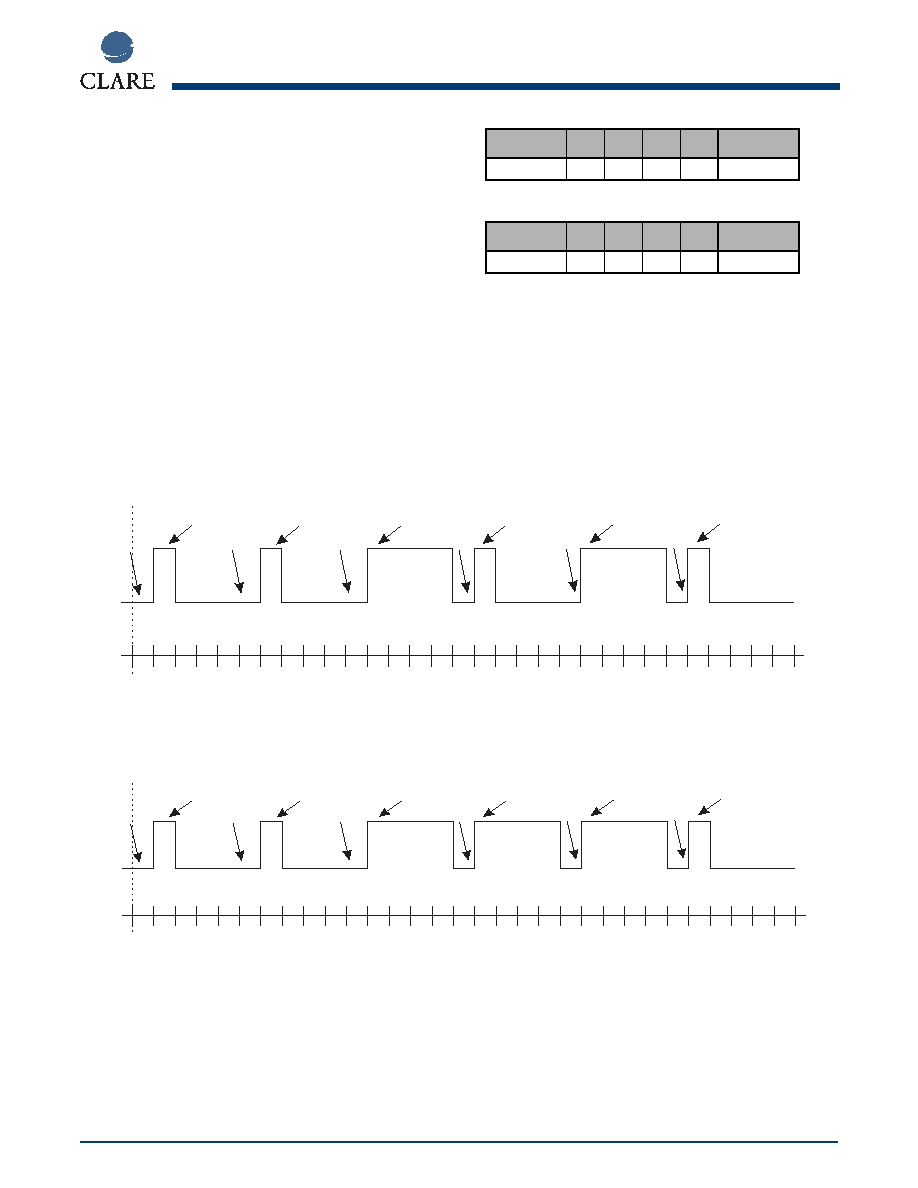
3.3 Programming Example
This programming example sets the following
CPC5601 output state, suitable for a European DAA:
3.3.1 LITELINK III
3.3.2 LITELINK II
1.
Hold the input low for 50
µ
S.
2.
Set the input high for 50
µ
S to trigger the timer.
3.
Set the input low for 150
µ
S to set output b1 to
off.
4.
Repeat the steps as shown in the programming
waveform below to program all six outputs to the
desired pattern.
Figure 8. LITELINK III European Programming Sample Input Waveform
Figure 9. LITELINK II European Programming Sample Input Waveform
4. Regulatory Information
CPC5601 can be used to build products that comply
with the requirements of TIA/EIA/IS-968 (formerly
FCC part 68), FCC part 15B, TBR-21, EN60950,
UL1950, EN55022B, IEC950/IEC60950, CISPR22B,
EN55024, and many other standards. CPC5601 com-
plies with the requirements of UL1577. CPC5601 pro-
vides supplementary isolation. Metallic surge
requirements are met through the inclusion of a Sidac-
tor in the application circuit. Longitudinal surge protec-
tion is provided by CPC5601's optical-across-the-
b1 (LSB)
b2
b3
b4
b5
b6 (MSB)
off
off
on
off
on
off
b1 (LSB)
b2
b3
b4
b5
b6 (MSB)
off
off
on
on
on
off
t0
50 S/div.
µ
setup
setup
setup
setup
setup
setup
timer
trigger
timer
trigger
timer
trigger
timer
trigger
timer
trigger
timer
trigger
bit 1
set off
bit 2
set off
bit 3
set on
bit 4
set off
bit 5
set on
bit 6
set off
t0
50 S/div.
µ
setup
setup
setup
setup
setup
setup
timer
trigger
timer
trigger
timer
trigger
timer
trigger
timer
trigger
timer
trigger
bit 1
set off
bit 2
set off
bit 3
set on
bit 4
set on
bit 5
set on
bit 6
set off

barrier technology and the use of high-voltage compo-
nents in the application circuit as needed.
The information provided in this document is intended
to inform the equipment designer but it is not sufficient
to assure proper system design or regulatory compli-
ance. Since it is the equipment manufacturer's respon-
sibility to have their equipment properly designed to
conform to all relevant regulations, designers using
CPC5601 are advised to carefully verify that their end-
product design complies with all applicable safety,
EMC, and other relevant standards and regulations.
Semiconductor components are not rated to withstand
electrical overstress or electro-static discharges result-
ing from inadequate protection measures at the board
or system level.
5. LITELINK Design Resources
5.1 Clare Design Resources
The Clare, Inc. web site has a wealth of information
useful for designing with LITELINK, including applica-
tion notes and reference designs that already meet all
applicable regulatory requirements. LITELINK data
sheets also contains additional application and design
information. See the following links:
LITELINK datasheets and reference designs
Application note AN-107
LOCxx Series - Isolated Ampli-
fier Design Principles
Application note AN-114
ITC117P
Application note AN-117
Customize Caller-ID Gain and
Ring Detect Voltage Threshold for CPC5610/11
Application note AN-140,
Understanding LITELINK
Application note AN-141,
Enhanced Pulse Dialing with
LITELINK
Application note AN-143,
Loop Reversal Detection with
LITELINK
Application note AN-146,
Guidelines for Effective
LITELINK Designs
Application note AN-147,
Worldwide Application of
LITELINK
Application note AN-149,
Increased LITELINK II Transmit
Power
Application note AN-150,
Ground-start Supervision Cir-
cuit Using IAA110
5.2 Third Party Design Resources
The following also contain information useful for
LITELINK designs. All of the books are available on
amazon.com
.
Understanding Telephone Electronics, Stephen J. Big-
elow, et. al., Butterworth-Heinenman; ISBN:
0750671750.
Newton's Telecom Dictionary, Harry Newton, CMP
Books; ISBN: 1578200695.
Photodiode Amplifiers: Op Amp Solutions, Jerald
Graeme, McGraw-Hill Professional Publishing; ISBN:
007024247X
Teccor, Inc.
Surge Protection Products
United States Code of Federal Regulations, CFR 47
Part 68.3.
For additional information please visit
www.clare.com
Clare, Inc. makes no representations or warranties with respect to the accuracy or completeness of the contents of this publication and reserves the right to make
changes to specifications and product descriptions at any time without notice. Neither circuit patent licenses or indemnity are expressed or implied. Except as set
forth in Clare's Standard Terms and Conditions of Sale, Clare, Inc. assumes no liability whatsoever, and disclaims any express or implied warranty relating to its
products, including, but not limited to, the implied warranty of merchantability, fitness for a particular purpose, or infringement of any intellectual property right.
The products described in this document are not designed, intended, authorized, or warranted for use as components in systems intended for surgical implant into
the body, or in other applications intended to support or sustain life, or where malfunction of Clare's product may result in direct physical harm, injury, or death to a
person or severe property or environmental damage. Clare, Inc. reserves the right to discontinue or make changes to its products at any time without notice.
Specifications: DS-CPC5601-R3.0
© Copyright 2002, Clare, Inc.
LITELINKTM is a trademark of Clare, Inc.
All rights reserved. Printed in USA.
6/5/2002