Preliminary Product Information
This document contains information for a new product.
Cirrus Logic reserves the right to modify this product without notice.
1
Copyright
©
Cirrus Logic, Inc. 2002
(All Rights Reserved)
P.O. Box 17847, Austin, Texas 78760
(512) 445 7222 FAX: (512) 445 7581
http://www.cirrus.com
CS5531/32/33/34
16-Bit and 24-Bit ADCs with Ultra Low Noise PGIA
Features
Chopper Stabilized PGIA (Programmable
Gain Instrumentation Amplifier, 1x to 64x)
6 nV/
Hz @ 0.1 Hz (No 1/f noise) at 64x
500 pA Input Current with Gains >1
Delta-Sigma Analog-to-Digital Converter
Linearity Error: 0.0007% FS
Noise Free Resolution: Up to 23 bits
Two or Four Channel Differential MUX
Scalable Input Span via Calibration
±5 mV to differential ±2.5V
Scalable V
REF
Input: Up to Analog Supply
Simple three-wire serial interface
SPI
®
and MicrowireTM Compatible
Schmitt Trigger on Serial Clock (SCLK)
R/W Calibration Registers Per Channel
Selectable Word Rates: 6.25 to 3,840 Sps
Selectable 50 or 60 Hz Rejection
Power Supply Configurations
VA+ = +5 V; VA- = 0 V; VD+ = +3 V to +5 V
VA+ = +2.5 V; VA- = -2.5 V; VD+ = +3 V to +5 V
VA+ = +3 V; VA- = -3 V; VD+ = +3 V
General Description
The CS5531/32/33/34 are highly integrated
Analog-
to-Digital Converters (ADCs) which use charge-balance
techniques to achieve 16-bit (CS5531/33) and 24-bit
(CS5532/34) performance. The ADCs are optimized for
measuring low-level unipolar or bipolar signals in weigh
scale,
process
control,
scientific,
and
medical
applications.
To accommodate these applications, the ADCs come as
either
two-channel
(CS5531/32)
or
four-channel
(CS5533/34) devices and include a very low noise chop-
per-stabilized instrumentation amplifier (6 nV/
Hz @ 0.1
Hz) with selectable gains of 1×, 2×, 4×, 8×, 16×, 32×, and
64×. These ADCs also include a fourth order
modu-
lator followed by a digital filter which provides twenty
selectable output word rates of 6.25, 7.5, 12.5, 15, 25, 30,
50, 60, 100, 120, 200, 240, 400, 480, 800, 960, 1600,
1920, 3200, and 3840 Sps (MCLK = 4.9152 MHz).
To ease communication between the ADCs and a micro-
controller, the converters include a simple three-wire se-
rial interface which is SPI and Microwire compatible with
a Schmitt Trigger input on the serial clock (SCLK).
High dynamic range, programmable output rates, and
flexible power supply options makes these ADCs ideal
solutions
for
weigh
scale
and
process
control
applications.
ORDERING INFORMATION
See page 48
VA+
C1
C2
VREF+
VREF-
VD+
DIFFERENTIAL
4
TH
ORDER
MODULATOR
PGIA
1,2,4,8,16
PROGRAMMABLE
SINC FIR FILTER
MUX
(CS5533/34
SHOWN)
AIN1+
AIN1-
AIN2+
AIN2-
AIN3+
AIN3-
AIN4+
AIN4-
SERIAL
INTERFACE
LATCH
CLOCK
GENERATOR
CALIBRATION
SRAM/CONTROL
LOGIC
DGND
CS
SDI
SDO
SCLK
OSC2
OSC1
A1
A0/GUARD
VA-
32,64
MAR `02
DS289PP5

CS5531/32/33/34
2
DS289PP5
TABLE OF CONTENTS
1.
CHARACTERISTICS AND SPECIFICATIONS ..........................................................5
ANALOG CHARACTERISTICS..........................................................................5
TYPICAL RMS NOISE (NV), CS5531/32/33/34-AS ...........................................8
TYPICAL NOISE FREE RESOLUTION(BITS), CS5532/34-AS .........................8
TYPICAL RMS NOISE (NV), CS5532/34-BS .....................................................9
TYPICAL NOISE FREE RESOLUTION(BITS), CS5532/34-BS .........................9
5 V DIGITAL CHARACTERISTICS ..................................................................10
3 V DIGITAL CHARACTERISTICS ..................................................................10
DYNAMIC CHARACTERISTICS ......................................................................11
ABSOLUTE MAXIMUM RATINGS ...................................................................11
SWITCHING CHARACTERISTICS ..................................................................12
2.
GENERAL DESCRIPTION .......................................................................................14
2.1.
Analog Input ....................................................................................................14
2.1.1. Analog Input Span .................................................................................... 15
2.1.2. Multiplexed Settling Limitations ............................................................15
2.1.3. Voltage Noise Density Performance .....................................................15
2.1.4. No Offset DAC ......................................................................................15
2.2.
Overview of ADC Register Structure and Operating Modes ............................16
2.2.1. System Initialization ..............................................................................17
2.2.2. Command Register Quick Reference ..................................................19
2.2.3. Command Register Descriptions ..........................................................20
2.2.4. Serial Port Interface ..............................................................................24
2.2.5. Reading/Writing On-Chip Registers ......................................................25
2.3.
Configuration Register .....................................................................................25
2.3.1. Power Consumption .............................................................................25
2.3.2. System Reset Sequence ......................................................................25
2.3.3. Input Short ............................................................................................26
2.3.4. Guard Signal .........................................................................................26
2.3.5. Voltage Reference Select .....................................................................26
2.3.6. Output Latch Pins .................................................................................26
2.3.7. Offset and Gain Select ..........................................................................27
Contacting Cirrus Logic Support
For a complete listing of Direct Sales, Distributor, and Sales Representative contacts, visit the Cirrus Logic web site at:
http://www.cirrus.com/corporate/contacts/sales.cfm
SPI is a registered trademark of International Business Machines Corporation.
Microwire is a trademark of National Semiconductor Corporation.
IMPORTANT NOTICE
"Preliminary" product information describes products that are in production, but for which full characterization data is not yet available. "Advance" product infor-
mation describes products that are in development and subject to development changes. Cirrus Logic, Inc. and its subsidiaries ("Cirrus") believe that the infor-
mation contained in this document is accurate and reliable. However, the information is subject to change without notice and is provided "AS IS" without warranty
of any kind (express or implied). Customers are advised to obtain the latest version of relevant information to verify, before placing orders, that information being
relied on is current and complete. All products are sold subject to the terms and conditions of sale supplied at the time of order acknowledgment, including those
pertaining to warranty, patent infringement, and limitation of liability. No responsibility is assumed by Cirrus for the use of this information, including use of this
information as the basis for manufacture or sale of any items, or for infringement of patents or other rights of third parties. This document is the property of Cirrus
and by furnishing this information, Cirrus grants no license, express or implied under any patents, mask work rights, copyrights, trademarks, trade secrets or
other intellectual property rights. Cirrus owns the copyrights of the information contained herein and gives consent for copies to be made of the information only
for use within your organization with respect to Cirrus integrated circuits or other parts of Cirrus. This consent does not extend to other copying such as copying
for general distribution, advertising or promotional purposes, or for creating any work for resale.
An export permit needs to be obtained from the competent authorities of the Japanese Government if any of the products or technologies described in this ma-
terial and controlled under the "Foreign Exchange and Foreign Trade Law" is to be exported or taken out of Japan. An export license and/or quota needs to be
obtained from the competent authorities of the Chinese Government if any of the products or technologies described in this material is subject to the PRC Foreign
Trade Law and is to be exported or taken out of the PRC.
CERTAIN APPLICATIONS USING SEMICONDUCTOR PRODUCTS MAY INVOLVE POTENTIAL RISKS OF DEATH, PERSONAL INJURY, OR SEVERE
PROPERTY OR ENVIRONMENTAL DAMAGE ("CRITICAL APPLICATIONS"). CIRRUS PRODUCTS ARE NOT DESIGNED, AUTHORIZED, OR WARRANT-
ED TO BE SUITABLE FOR USE IN LIFE-SUPPORT DEVICES OR SYSTEMS OR OTHER CRITICAL APPLICATIONS. INCLUSION OF CIRRUS PRODUCTS
IN SUCH APPLICATIONS IS UNDERSTOOD TO BE FULLY AT THE CUSTOMER'S RISK.
Cirrus Logic, Cirrus, and the Cirrus Logic logo designs are trademarks of Cirrus Logic, Inc. All other brand and product names in this document may be trade-
marks or service marks of their respective owners.

CS5531/32/33/34
DS289PP5
3
2.3.8. Filter Rate Select .................................................................................. 27
2.3.9. Configuration Register Descriptions ..................................................... 28
2.4.
Setting up the CSRs for a Measurement ......................................................... 29
2.4.1. Channel-Setup Register Descriptions ................................................. 30
2.5.
Calibration ....................................................................................................... 32
2.5.1. Calibration Registers ............................................................................ 32
2.5.2. Gain Register ...................................................................................... 32
2.5.3. Offset Register .................................................................................... 32
2.5.4. Performing Calibrations ........................................................................ 33
2.5.5. Self Calibration ..................................................................................... 33
2.5.6. System Calibration ............................................................................... 34
2.5.7. Calibration Tips .................................................................................... 34
2.5.8. Limitations in Calibration Range ........................................................... 35
2.6.
Performing Conversions .................................................................................. 35
2.6.1. Single Conversion Mode ...................................................................... 35
2.6.2. Continuous Conversion Mode .............................................................. 36
2.6.3. Examples of Using CSRs to Perform Conversions and Calibrations ... 37
2.7.
Using Multiple ADCs Synchronously ............................................................... 38
2.8.
Conversion Output Coding .............................................................................. 38
2.8.1. Conversion Data Output Descriptions .................................................. 39
2.9.
Digital Filter ..................................................................................................... 40
2.10. Clock Generator .............................................................................................. 41
2.11. Power Supply Arrangements ........................................................................... 41
2.12. Getting Started ................................................................................................ 45
2.13. PCB Layout ..................................................................................................... 45
3.
PIN DESCRIPTIONS ............................................................................................... 46
Clock Generator .............................................................................................. 46
Control Pins and Serial Data I/O ..................................................................... 46
Measurement and Reference Inputs ............................................................... 47
Power Supply Connections ............................................................................. 47
4.
SPECIFICATION DEFINITIONS ............................................................................... 48
5.
ORDERING GUIDE .................................................................................................. 48
6.
PACKAGE DRAWINGS ........................................................................................... 49

CS5531/32/33/34
4
DS289PP5
LIST OF FIGURES
Figure 1. SDI Write Timing (Not to Scale) ...............................................................................13
Figure 2. SDO Read Timing (Not to Scale) .............................................................................13
Figure 3. Multiplexer Configuration .........................................................................................14
Figure 4. Input models for AIN+ and AIN- pins .......................................................................15
Figure 5. Measured Voltage Noise Density .............................................................................15
Figure 6. CS5531/32/33/34 Register Diagram ........................................................................16
Figure 7. Command and Data Word Timing............................................................................24
Figure 8. Guard Signal Shielding Scheme ..............................................................................26
Figure 9. Input Reference Model when VRS = 1.....................................................................27
Figure 10. Input Reference Model when VRS = 0...................................................................27
Figure 11. Self Calibration of Offset ........................................................................................34
Figure 12. Self Calibration of Gain ..........................................................................................34
Figure 13. System Calibration of Offset ..................................................................................34
Figure 14. System Calibration of Gain ....................................................................................34
Figure 15. Synchronizing Multiple ADCs.................................................................................38
Figure 16. Digital Filter Response (Word Rate = 60 Sps) .......................................................40
Figure 17. 120 Sps Filter Magnitude Plot to 120 Hz................................................................40
Figure 18. 120 Sps Filter Phase Plot to 120 Hz ......................................................................40
Figure 19. Z-Transforms of Digital Filters ................................................................................40
Figure 20. On-chip Oscillator Model ........................................................................................41
Figure 21. CS5532 Configured with a Single +5 V Supply......................................................42
Figure 22. CS5532 Configured with ±2.5 V Analog Supplies..................................................43
Figure 23. CS5532 Configured with ±3 V Analog Supplies .....................................................43
Figure 24. CS5532 Configured for Thermocouple Measurement ...........................................44
Figure 25. Bridge with Series Resistors ..................................................................................44
LIST OF TABLES
Table 1. Conversion Timing for Single Mode ..........................................................................36
Table 2. Conversion Timing for Continuous Mode ..................................................................37
Table 3. Command Byte Pointer .............................................................................................37
Table 4. Output Coding for 16-bit CS5531 and CS5533 .........................................................39
Table 5. Output Coding for 24-bit CS5532 and CS5534 .........................................................39

CS5531/32/33/34
DS289PP5
5
1. CHARACTERISTICS AND SPECIFICATIONS
ANALOG CHARACTERISTICS
(VA+, VD+ = 5 V ±5%; VREF+ = 5 V; VA-, VREF-, DGND = 0 V;
MCLK = 4.9152 MHz; OWR (Output Word Rate) = 60 Sps; Bipolar Mode; Gain = 32)
(See Notes 1 and 2.)
Notes: 1. Applies after system calibration at any temperature within -40 °C ~ +85 °C.
2. Specifications guaranteed by design, characterization, and/or test. LSB is 16 bits for the CS5531/33 and
LSB is 24 bits for the CS5532/34.
3.
This specification applies to the device only and does not include any effects by external parasitic
thermocouples. The PGIA contributes 5 nV of offset drift, and the modulator contributes 640/G nV of
offset drift, where G is the amplifier gain setting.
4. Drift over specified temperature range after calibration at power-up at 25 °C.
Parameter
CS5531-AS/CS5533-AS
Unit
Min
Typ
Max
Accuracy
Linearity Error
-
±
0.0015
±
0.003
%FS
No Missing Codes
16
-
-
Bits
Bipolar Offset
-
±
1
±2
LSB
16
Unipolar Offset
-
±
2
±
4
LSB
16
Offset Drift
(Notes 3 and 4)
-
640/G + 5
-
nV/°C
Bipolar Full Scale Error
-
±
8
±
31
ppm
Unipolar Full Scale Error
-
±
16
±
62
ppm
Full Scale Drift
(Note 4)
-
2
-
ppm/°C
Parameter
CS5532-AS/CS5534-AS
CS5532-BS/CS5534-BS
Unit
Min
Typ
Max
Min
Typ
Max
Accuracy
Linearity Error
-
±
0.0015
±
0.003
-
±
0.0007
±
0.0015
%FS
No Missing Codes
24
-
-
24
-
-
Bits
Bipolar Offset
-
±
16
±32
-
±
16
±32
LSB
24
Unipolar Offset
-
±
32
±
64
-
±
32
±
64
LSB
24
Offset Drift
(Notes 3 and 4)
-
640/G + 5
-
-
640/G + 5
-
nV/°C
Bipolar Full Scale Error
-
±
8
±
31
-
±
8
±
31
ppm
Unipolar Full Scale Error
-
±
16
±
62
-
±
16
±
62
ppm
Full Scale Drift
(Note 4)
-
TBD
-
-
2
-
ppm/°C
CS5531/32/33/34
6
DS289PP5
ANALOG CHARACTERISTICS
(Continued) (See Notes 1 and 2.)
Notes: 5. The voltage on the analog inputs is amplified by the PGIA, and becomes V
CM
±
Gain*(AIN+ - AIN-)/2 at
the differential outputs of the amplifier. In addition to the input common mode + signal requirements for
the analog input pins, the differential outputs of the amplifier must remain between (VA- + 0.1 V) and
(VA+ - 0.1 V) to avoid saturation of the output stage.
6. See the section of the data sheet which discusses input models.
Parameter
Min
Typ
Max
Unit
Analog Input
Common Mode + Signal on AIN+ or AIN-Bipolar/Unipolar Mode
Gain = 1
Gain = 2, 4, 8, 16, 32, 64
(Note 5)
VA-
VA- + 0.7
-
-
VA+
VA+ - 1.7
V
V
CVF Current on AIN+ or AIN-
Gain = 1
(Note 6)
Gain = 2, 4, 8, 16, 32, 64
-
-
500
500
-
-
nA
pA
Input Current Noise
Gain = 1
Gain = 2, 4, 8, 16, 32, 64
-
-
200
1
-
-
pA/
Hz
pA/
Hz
Input Leakage for Mux when Off (at 25 °C)
-
10
-
pA
Off-Channel Mux Isolation
-
120
-
dB
Open Circuit Detect Current
100
300
-
nA
Common Mode Rejection
dc, Gain = 1
dc, Gain = 64
50, 60 Hz
-
-
-
90
130
120
-
-
-
dB
dB
dB
Input Capacitance
-
60
-
pF
Guard Drive Output
-
20
-
µA
Voltage Reference Input
Range
(VREF+) - (VREF-)
1
2.5
(VA+)-(VA-)
V
CVF Current
(Note 6)
-
500
-
nA
Common Mode Rejection
dc
50, 60 Hz
-
-
120
120
-
-
dB
dB
Input Capacitance
11
-
22
pF
System Calibration Specifications
Full Scale Calibration Range
Bipolar/Unipolar Mode
3
-
110
%FS
Offset Calibration Range
Bipolar Mode
-100
-
100
%FS
Offset Calibration Range
Unipolar Mode
-90
-
90
%FS

CS5531/32/33/34
DS289PP5
7
ANALOG CHARACTERISTICS
(Continued) (See Notes 1 and 2.)
7. All outputs unloaded. All input CMOS levels.
8. Power is specified when the instrumentation amplifier (Gain
2) is on. Analog supply current is reduced
by approximately 1/2 when the instrumentation amplifier is off (Gain = 1).
9. Tested with 100 mV change on VA+ or VA-.
Parameter
CS5531/32/33/34-AS
CS5532/34-BS
Min
Typ
Max
Min
Typ
Max
Unit
Power Supplies
DC Power Supply Currents (Normal Mode)
I
A+,
I
A-
I
D+
-
-
6
0.5
8
1
-
-
13
0.5
15
1
mA
mA
Power Consumption
Normal Mode (Notes 7 and 8)
Standby
Sleep
-
-
-
35
3
500
45
-
-
-
-
-
70
4
500
80
-
-
mW
mW
µW
Power Supply Rejection
(Note 9)
dc Positive Supplies
dc Negative Supply
-
-
115
115
-
-
-
-
115
115
-
-
dB
dB

CS5531/32/33/34
8
DS289PP5
TYPICAL RMS NOISE (nV), CS5531/32/33/34-AS
(See notes 10, 11 and 12)
Notes: 10. Wideband noise aliased into the baseband. Referred to the input. Typical values shown for 25 °C.
11. For Peak-to-Peak Noise multiply by 6.6 for all ranges and output rates.
12. Word rates and -3dB points with FRS = 0. When FRS = 1, word rates and -3dB points scale by 5/6.
TYPICAL NOISE FREE RESOLUTION(BITS), CS5532/34-AS
(See Notes 13 and 14)
13. Noise Free Resolution listed is for Bipolar operation, and is calculated as LOG((Input Span)/(6.6xRMS
Noise))/LOG(2) rounded to the nearest bit. For Unipolar operation, the input span is 1/2 as large, so one
bit is lost. The input span is calculated in the analog input span section of the data sheet. The Noise
Free Resolution table is computed with a value of 1.0 in the gain register. Values other than 1.0 will
scale the noise, and change the Noise Free Resolution accordingly.
14. "Noise Free Resolution" is not the same as "Effective Resolution". Effective Resolution is based on the
RMS noise value, while Noise Free Resolution is based on a peak-to-peak noise value specified as 6.6
times the RMS noise value. Effective Resolution is calculated as LOG((Input Span)/(RMS
Noise))/LOG(2).
Specifications are subject to change without notice.
Output Word
Rate (Sps)
-3 dB Filter
Frequency (Hz)
Instrumentation Amplifier Gain
x64
x32
x16
x8
x4
x2
x1
7.5
1.94
17
17
19
26
42
79
155
15
3.88
24
25
27
36
59
111
218
30
7.75
34
35
39
51
84
157
308
60
15.5
48
49
54
72
118
222
436
120
31
68
70
77
102
167
314
616
240
62
115
160
276
527
1040
2070
4150
480
122
163
230
392
748
1480
2950
5890
960
230
229
321
554
1060
2090
4170
8340
1,920
390
344
523
946
1840
3650
7290
14600
3,840
780
1390
2710
5390
10800
21500
43000
86100
Output Word
Rate (Sps)
-3 dB Filter
Frequency (Hz)
Instrumentation Amplifier Gain
x64
x32
x16
x8
x4
x2
x1
7.5
1.94
19
20
21
22
22
22
22
15
3.88
19
20
21
21
21
22
22
30
7.75
18
19
20
21
21
21
21
60
15.5
18
19
20
20
20
21
21
120
31
17
18
19
20
20
20
20
240
62
16
17
17
17
17
17
17
480
122
16
17
17
17
17
17
17
960
230
15
16
16
16
16
16
16
1,920
390
15
15
15
15
15
15
15
3,840
780
13
13
13
13
13
13
13
CS5531/32/33/34
DS289PP5
9
TYPICAL RMS NOISE (nV), CS5532/34-BS
(See notes 15, 16, 17 and 18)
Notes: 15. The -B devices provide the best noise specifications.
16. Wideband noise aliased into the baseband. Referred to the input. Typical values shown for 25 °C.
17. For Peak-to-Peak Noise multiply by 6.6 for all ranges and output rates.
18. Word rates and -3dB points with FRS = 0. When FRS = 1, word rates and -3dB points scale by 5/6.
TYPICAL NOISE FREE RESOLUTION(BITS), CS5532/34-BS
(See Notes 19 and 20)
19. Noise Free Resolution listed is for Bipolar operation, and is calculated as LOG((Input Span)/(6.6xRMS
Noise))/LOG(2) rounded to the nearest bit. For Unipolar operation, the input span is 1/2 as large, so one
bit is lost. The input span is calculated in the analog input span section of the data sheet. The Noise
Free Resolution table is computed with a value of 1.0 in the gain register. Values other than 1.0 will scale
the noise, and change the Noise Free Resolution accordingly.
20. "Noise Free Resolution" is not the same as "Effective Resolution". Effective Resolution is based on the
RMS noise value, while Noise Free Resolution is based on a peak-to-peak noise value specified as 6.6
times the RMS noise value. Effective Resolution is calculated as LOG((Input Span)/(RMS
Noise))/LOG(2).
Specifications are subject to change without notice.
Output Word
Rate (Sps)
-3 dB Filter
Frequency (Hz)
Instrumentation Amplifier Gain
x64
x32
x16
x8
x4
x2
x1
7.5
1.94
8.5
9
10
15
26
50
99
15
3.88
12
13
15
21
37
70
139
30
7.75
17
18
21
30
52
99
196
60
15.5
24
25
29
42
73
140
277
120
31
34
36
42
59
103
198
392
240
62
80
136
260
514
1020
2050
4090
480
122
113
194
369
730
1450
2900
5810
960
230
159
274
523
1030
2060
4110
8230
1,920
390
260
470
912
1810
3620
7230
14500
3,840
780
1360
2690
5380
10800
21500
43000
86000
Output Word
Rate (Sps)
-3 dB Filter
Frequency (Hz)
Instrumentation Amplifier Gain
x64
x32
x16
x8
x4
x2
x1
7.5
1.94
20
21
22
23
23
23
23
15
3.88
20
21
22
22
22
22
22
30
7.75
19
20
21
22
22
22
22
60
15.5
19
20
21
21
21
21
21
120
31
18
19
20
21
21
21
21
240
62
17
17
18
18
18
18
18
480
122
17
17
17
17
17
17
17
960
230
16
16
17
17
17
17
17
1,920
390
16
16
16
16
16
16
16
3,840
780
13
13
13
13
13
13
13

CS5531/32/33/34
10
DS289PP5
5 V DIGITAL CHARACTERISTICS
(VA+, VD+ = 5 V ±5%; VA-, DGND = 0 V;
See Notes 2 and 21.)
3 V DIGITAL CHARACTERISTICS
(T
A
= 25 °C; VA+ = 5V ±5%; VD+ = 3.0V±10%; VA-, DGND =
0V; See Notes 2 and 21.)
21. All measurements performed under static conditions.
Parameter
Symbol
Min
Typ
Max
Unit
High-Level Input Voltage
All Pins Except SCLK
SCLK
V
IH
0.6 VD+
(VD+) - 0.45
-
-
VD+
VD+
V
Low-Level Input Voltage
All Pins Except SCLK
SCLK
V
IL
0.0
0.0
-
0.8
0.6
V
High-Level Output Voltage
A0 and A1, I
out
= -1.0 mA
SDO, I
out
= -5.0 mA
V
OH
(VA+) - 1.0
(VD+) - 1.0
-
-
V
Low-Level Output Voltage
A0 and A1, I
out
= 1.0 mA
SDO, I
out
= 5.0 mA
V
OL
-
-
(VA-) + 0.4
0.4
V
Input Leakage Current
I
in
-
±1
±10
µA
SDO 3-State Leakage Current
I
OZ
-
-
±10
µA
Digital Output Pin Capacitance
C
out
-
9
-
pF
Parameter
Symbol
Min
Typ
Max
Unit
High-Level Input Voltage
All Pins Except SCLK
SCLK
V
IH
0.6 VD+
(VD+) - 0.45
-
VD+
VD+
V
Low-Level Input Voltage
All Pins Except SCLK
SCLK
V
IL
0.0
0.0
-
0.8
0.6
V
High-Level Output Voltage
A0 and A1, I
out
= -1.0 mA
SDO, I
out
= -5.0 mA
V
OH
(VA+) - 1.0
(VD+) - 1.0
-
-
V
Low-Level Output Voltage
A0 and A1, I
out
= 1.0 mA
SDO, I
out
= 5.0 mA
V
OL
-
-
(VA-) + 0.4
0.4
V
Input Leakage Current
I
in
-
±1
±10
µA
SDO 3-State Leakage Current
I
OZ
-
-
±10
µA
Digital Output Pin Capacitance
C
out
-
9
-
pF

CS5531/32/33/34
DS289PP5
11
DYNAMIC CHARACTERISTICS
22. The ADCs use a Sinc
5
filter for the 3200 Sps and 3840 Sps output word rate (OWR) and a Sinc
5
filter
followed by a Sinc
3
filter for the other OWRs. OWR
sinc5
refers to the 3200 Sps (FRS = 1) or 3840 Sps
(FRS = 0) word rate associated with the Sinc
5
filter.
23. The single conversion mode only outputs fully settled conversions. See Table 1 for more details about
single conversion mode timing. OWR
SC
is used here to designate the different conversion time
associated with single conversions.
24. The continuous conversion mode outputs every conversion. This means that the filter's settling time
with a full scale step input in the continuous conversion mode is dictated by the OWR.
ABSOLUTE MAXIMUM RATINGS
(DGND = 0 V; See Note 25.)
Notes: 25. All voltages with respect to ground.
26. VA+ and VA- must satisfy {(VA+) - (VA-)}
+6.6 V.
27. VD+ and VA- must satisfy {(VD+) - (VA-)}
+7.5 V.
28. Applies to all pins including continuous overvoltage conditions at the analog input (AIN) pins.
29. Transient current of up to 100 mA will not cause SCR latch-up. Maximum input current for a power
supply pin is ±50 mA.
30. Total power dissipation, including all input currents and output currents.
WARNING: Operation at or beyond these limits may result in permanent damage to the device.
Normal operation is not guaranteed at these extremes.
Parameter
Symbol
Ratio
Unit
Modulator Sampling Rate
f
s
MCLK/16
Sps
Filter Settling Time to 1/2 LSB (Full Scale Step Input)
Single Conversion mode
(Notes 22, 23, and 24)
Continuous Conversion mode, OWR < 3200 Sps
Continuous Conversion mode, OWR
3200 Sps
t
s
t
s
t
s
1/OWR
SC
5/OWR
sinc5
+ 3/OWR
5/OWR
s
s
s
Parameter
Symbol
Min
Typ
Max
Unit
DC Power Supplies
(Notes 26 and 27)
Positive Digital
Positive Analog
Negative Analog
VD+
VA+
VA-
-0.3
-0.3
+0.3
-
-
-
+6.0
+6.0
-3.75
V
V
V
Input Current, Any Pin Except Supplies
(Notes 28 and 29)
I
IN
-
-
±10
mA
Output Current
I
OUT
-
-
±25
mA
Power Dissipation
(Note 30)
PDN
-
-
500
mW
Analog Input Voltage
VREF pins
AIN Pins
V
INR
V
INA
(VA-) -0.3
(VA-) -0.3
-
-
(VA+) + 0.3
(VA+) + 0.3
V
V
Digital Input Voltage
V
IND
-0.3
-
(VD+) + 0.3
V
Ambient Operating Temperature
T
A
-40
-
85
°C
Storage Temperature
T
stg
-65
-
150
°C

CS5531/32/33/34
12
DS289PP5
SWITCHING CHARACTERISTICS
(VA+ = 2.5 V or 5 V ±5%; VA- = -2.5V±5% or 0 V; VD+ = 3.0 V
±10% or 5 V ±5%;DGND = 0 V; Levels: Logic 0 = 0 V, Logic 1 = VD+; C
L
= 50 pF;
See Figures 1 and 2.)
Notes: 31. Device parameters are specified with a 4.9152 MHz clock.
32. Specified using 10% and 90% points on waveform of interest. Output loaded with 50 pF.
33. Oscillator start-up time varies with crystal parameters. This specification does not apply when using an
external clock source.
Parameter
Symbol
Min
Typ
Max
Unit
Master Clock Frequency
(Note 31)
External Clock or Crystal Oscillator
MCLK
1
4.9152
5
MHz
Master Clock Duty Cycle
40
-
60
%
Rise Times
(Note 32)
Any Digital Input Except SCLK
SCLK
Any Digital Output
t
rise
-
-
-
-
-
50
1.0
100
-
µs
µs
ns
Fall Times
(Note 32)
Any Digital Input Except SCLK
SCLK
Any Digital Output
t
fall
-
-
-
-
-
50
1.0
100
-
µs
µs
ns
Start-up
Oscillator Start-up Time
XTAL = 4.9152 MHz
(Note 33)
t
ost
-
20
-
ms
Serial Port Timing
Serial Clock Frequency
SCLK
0
-
2
MHz
Serial Clock
Pulse Width High
Pulse Width Low
t
1
t
2
250
250
-
-
-
-
ns
ns
SDI Write Timing
CS Enable to Valid Latch Clock
t
3
50
-
-
ns
Data Set-up Time prior to SCLK rising
t
4
50
-
-
ns
Data Hold Time After SCLK Rising
t
5
100
-
-
ns
SCLK Falling Prior to CS Disable
t
6
100
-
-
ns
SDO Read Timing
CS to Data Valid
t
7
-
-
150
ns
SCLK Falling to New Data Bit
t
8
-
-
150
ns
CS Rising to SDO Hi-Z
t
9
-
-
150
ns

CS5531/32/33/34
DS289PP5
13
C S
S C L K
M S B
M S B -1
L S B
S D I
t3
t6
t4
t5
t1
t2
000
000
000
000
000
000
000
000
000
000
000
000
000
000
000
000
000
000
000
000
000
000
000
000
000
000
000
000
000
000
000
000
Figure 1. SDI Write Timing (Not to Scale)
C S
S C LK
M S B
M S B -1
LS B
S D O
t7
t9
t8
t1
t2
000
000
000
000
000
000
000
000
000
000
000
000
000
000
000
000
000
000
000
000
000
000
000
000
000
000
000
000
000
000
000
000
000
Figure 2. SDO Read Timing (Not to Scale)

CS5531/32/33/34
14
DS289PP5
2. GENERAL DESCRIPTION
The CS5531/32/33/34 are highly integrated
An-
alog-to-Digital Converters (ADCs) which use
charge-balance
techniques
to
achieve
16-bit
(CS5531/33) and 24-bit (CS5532/34) performance.
The ADCs are optimized for measuring low-level
unipolar or bipolar signals in weigh scale, process
control, scientific, and medical applications.
To accommodate these applications, the ADCs
come as either two-channel (CS5531/32) or four-
channel (CS5533/34) devices and include a very
low noise chopper-stabilized programmable gain
instrumentation amplifier (PGIA, 6 nV/
Hz @ 0.1
Hz) with selectable gains of 1×, 2×, 4×, 8×, 16×,
32×, and 64×. These ADCs also include a fourth or-
der
modulator followed by a digital filter which
provides twenty selectable output word rates of 6.25,
7.5, 12.5, 15, 25, 30, 50, 60, 100, 120, 200, 240, 400,
480, 800, 960, 1600, 1920, 3200, and 3840 Samples
per second (MCLK = 4.9152 MHz).
To ease communication between the ADCs and a
micro-controller, the converters include a simple
three-wire serial interface which is SPI and Mi-
crowire compatible with a Schmitt Trigger input on
the serial clock (SCLK).
2.1. Analog Input
Figure 3 illustrates a block diagram of the
CS5531/32/33/34. The front end consists of a multi-
plexer, a unity gain coarse/fine charge input buffer,
and a programmable gain chopper-stabilized instru-
mentation amplifier. The unity gain buffer is activat-
ed any time conversions are performed with a gain
of one and the instrumentation amplifier is activated
any time conversions are performed with gain set-
tings greater than one.
The unity gain buffer is designed to accommodate
rail to rail input signals. The common-mode plus
signal range for the unity gain buffer amplifier is
VA- to VA+. Typical CVF (sampling) current for
the unity gain buffer amplifier is about 500 nA
(MCLK = 4.9152 MHz, see Figure 4).
The instrumentation amplifier is chopper-stabi-
lized and operates with a chop clock frequency of
MCLK/128. The CVF (sampling) current into the
instrumentation amplifier is typically 500 pA over
VREF+
Sinc
Digital
Filter
XGAIN
M
U
X
AIN2+
AIN2-
AIN1+
AIN1-
CS5531/32 IN+
IN-
AIN4+
AIN4-
*
*
*
AIN1+
AIN1-
CS5533/34
M
U
X
IN+
IN-
IN+
IN-
GAIN is the gain setting of the PGIA (i.e. 2, 4, 8, 16, 32, 64)
X1
X1
X1
VREF-
X1
Differential
4
Order
Modulator
th
5
Programmable
Sinc
Digital Filter
3
Serial
Port
1000
1000
22 nF
C1 PIN
C2 PIN
Figure 3. Multiplexer Configuration
CS5531/32/33/34
DS289PP5
15
-40°C to +85°C (MCLK=4.9152 MHz). The com-
mon-mode plus signal range of the instrumentation
amplifier is (VA-) + 0.7 V to (VA+) - 1.7 V.
Figure 4 illustrates the input models for the ampli-
fiers. The dynamic input current for each of the
pins can be determined from the models shown.
Note:
The C=2.5pF and C = 16pF capacitors are for
input current modeling only. For physical
input capacitance see `Input Capacitance'
specification under Analog Characteristics.
2.1.1. Analog Input Span
The full scale input signal that the converter can dig-
itize is a function of the gain setting and the refer-
ence voltage connected between the VREF+ and
VREF- pins. The full scale input span of the convert-
er is ((VREF+) - (VREF-))/(GxA), where G is the
gain of the amplifier and A is 2 for VRS = 0, or A is
1 for VRS = 1. VRS is the Voltage Reference Select
bit, and must be set according to the differential volt-
age applied to the VREF+ and VREF- pins on the
part. See section 2.3.5 for more details.
After reset, the unity gain buffer is engaged. With a
2.5V reference this would make the full scale input
range default to 2.5 V. By activating the instrumen-
tation amplifier (i.e. a gain setting other than 1) and
using a gain setting of 32, the full scale input range
can quickly be set to 2.5/32 or about 78 mV. Note
that these input ranges assume the calibration regis-
ters are set to their default values (i.e. Gain = 1.0 and
Offset = 0.0).
2.1.2. Multiplexed Settling Limitations
The settling performance of the CS5531/32/33/34
in multiplexed applications is affected by the sin-
gle-pole low-pass filter which follows the instru-
mentation amplifier (see Figure 3). To achieve data
sheet settling and linearity specifications, it is rec-
ommended that a 22 nF C0G capacitor be used. Ca-
pacitors as low as 10 nF or X7R type capacitors can
also be used with some minor increase in distortion
for AC signals.
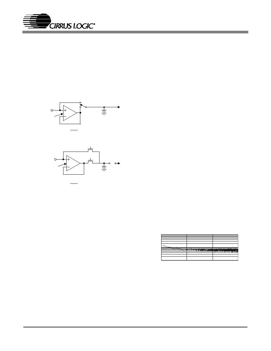
2.1.3. Voltage Noise Density Performance
Figure 5 illustrates the measured voltage noise den-
sity versus frequency from 0.01 Hz to 10 Hz of a
CS5532-BS. The device was powered with ±2.5 V
supplies, using 120 Sps OWR, the 64x gain range,
bipolar mode, and with the input short bit enabled.
2.1.4. No Offset DAC
An offset DAC was not included in the CS553X
family because the high dynamic range of the con-
verter eliminates the need for one. The offset regis-
AIN
Gain = 2, 4, 8, 16, 32, 64
C =12.5 pF
f =
Gain = 1
AIN
C = 80 pF
Coarse
1
Fine
1
V
20 mV
i = fV
C
os
os
n
V
1 mV
i = fV
C
os
os
n
MCLK
128
f =
MCLK
16
Figure 4. Input models for AIN+ and AIN- pins
1
10
100
0.01
0.1
1
10
Frequency (Hz)
nV
/
Hz
Gain = 64
Figure 5. Measured Voltage Noise Density

CS5531/32/33/34
16
DS289PP5
ter can be manipulated by the user to mimic the
function of a DAC if desired.
2.2. Overview of ADC Register Structure
and Operating Modes
The CS5531/32/33/34 ADCs have an on-chip con-
troller, which includes a number of user-accessible
registers. The registers are used to hold offset and
gain calibration results, configure the chip's operat-
ing modes, hold conversion instructions, and to
store conversion data words. Figure 6 depicts a
block diagram of the on-chip controller's internal
registers.
Each of the converters has 32-bit registers to func-
tion as offset and gain calibration registers for each
channel. The converters with two channels have
two offset and two gain calibration registers, the
converters with four channels have four offset and
four gain calibration registers. These registers hold
calibration results. The contents of these registers
can be read or written by the user. This allows cal-
ibration data to be off-loaded into an external EE-
PROM. The user can also manipulate the contents
of these registers to modify the offset or the gain
slope of the converter.
The converters include a 32-bit configuration reg-
ister which is used for setting options such as the
power down modes, resetting the converter, short-
ing the analog inputs, and enabling diagnostic test
bits like the guard signal.
A group of registers, called Channel Setup Regis-
ters, are used to hold pre-loaded conversion in-
structions. Each channel setup register is 32 bits
long, and holds two 16-bit conversion instructions
referred to as Setups. Upon power up, these regis-
ters can be initialized by the system microcontrol-
ler with conversion instructions. The user can then
instruct the converter to perform single or multiple
conversions or calibrations with the converter in
the mode defined by one of these Setups.
Offset 1 (1 x 32)
Offset 2 (1 x 32)
Offset 3 (1 x 32)
Offset 4 (1 x 32)
Gain 1 (1 x 32)
Gain 2 (1 x 32)
Gain 3 (1 x 32)
Gain 4 (1 x 32)
Setup 1
(1 x 16)
Setup 2
(1 x 16)
Setup 4
(1 x 16)
Setup 6
(1 x 16)
Setup 8
(1 x 16)
Setup 3
(1 x 16)
Setup 5
(1 x 16)
Setup 7
(1 x 16)
Offset Registers (4 x 32)
Gain R egisters (4 x 32)
Channel Setup
Registers (4 x 32)
Conversion Data
Register (1 x 32)
Con figuration Register (1 x 32)
Power S ave Select
Reset System
Input Short
Guard Signal
Voltage Reference Select
Output Latch
Output Latch Select
Channel Select
Gain
W ord Rate
Unipolar/Bipolar
Output Latch
Delay Time
Open Circuit Detect
CS
SDI
SDO
SCLK
R
ead
O
n
l
y
Com mand
Register (1 × 8)
Wr
i
t
e
O
n
l
y
Serial
Interface
Data (1 x 32)
Offset/Gain Select
Filter Rate Select
Offset/Gain Pointer
Figure 6. CS5531/32/33/34 Register Diagram

CS5531/32/33/34
DS289PP5
17
Using the single conversion mode, an 8-bit com-
mand word can be written into the serial port. The
command includes pointer bits which `point' to a
16-bit command in one of the Channel Setup Reg-
isters which is to be executed. The 16-bit Setups
can be programmed to perform a conversion on any
of the input channels of the converter. More than
one of the 16-bit Setups can be used for the same
analog input channel. This allows the user to con-
vert on the same signal with either a different con-
version speed, a different gain range, or any of the
other options available in the channel setup regis-
ters. Alternately, the user can set up the registers to
perform different conversion conditions on each of
the input channels.
The ADCs also include continuous conversion ca-
pability. The ADCs can be instructed to continu-
ously convert, referencing one 16-bit command
Setup. In the continuous conversions mode, the
conversion data words are loaded into a shift regis-
ter. The converter issues a flag on the SDO pin
when a conversion cycle is completed so the user
can read the register, if need be. See the section on
Performing Conversions for more details.
The following pages document how to initialize the
converter, perform offset and gain calibrations, and
how to configure the converter for the various con-
version modes. Each of the bits of the configuration
register and of the Channel Setup Registers is de-
scribed. A list of examples follows the description
section. Also the Command Register Quick Refer-
ence can be used to decode all valid commands (the
first 8-bits into the serial port).
2.2.1. System Initialization
The CS5531/32/33/34 provide no power-on-reset
function. To initialize the ADCs, the user must per-
form a software reset by resetting the ADC's serial
port with the Serial Port Initialization sequence.
This sequence resets the serial port to the command
mode and is accomplished by transmitting at least
15 SYNC1 command bytes (0xFF hexadecimal),
followed by one SYNC0 command (0xFE hexa-
decimal). Note that this sequence can be initiated at
anytime to reinitialize the serial port. To complete
the system initialization sequence, the user must
also perform a system reset sequence which is as
follows: Write a logic 1 into the RS bit of the con-
figuration register. This will reset the calibration
registers and other logic (but not the serial port). A
valid reset will set the RV bit in the configuration
register to a logic 1. After writing the RS bit to a
logic 1, wait 20 microseconds, then write the RS bit
back to logic 0. While this involves writing an en-
tire word into the configuration register, the RV bit
is a read only bit, therefore a write to the configu-
ration register will not overwrite the RV bit. After
clearing the RS bit back to logic 0, read the config-
uration register to check the state of the RV bit as
this indicates that a valid reset occurred. Reading
the configuration register clears the RV bit back to
logic 0.
Completing the reset cycle initializes the on-chip
registers to the following states:
Note:
Previous datasheets stated that the RS bit
would clear itself back to logic 0 and therefore
the user was not required to write the RS bit
back to logic 0. The current data sheet
instruction that requires the user to write into
the configuration register to clear the RS bit
has been added to insure that the RS bit is
cleared. Characterization across multiple lots
of silicon has indicated some chips do not
automatically reset the RS bit to logic 0 in the
configuration register, although the reset
function is completed. This occurs only on
small number of chips when the VA- supply is
negative with respect to DGND. This has not
caused an operational issue for customers
because their start-up sequence includes
writing a word (with RS=0) into the
configuration register after performing a
reset. The change in the reset sequence to
Configuration Register:
00000000(H)
Offset Registers:
00000000(H)
Gain Registers:
01000000(H)
Channel Setup Registers: 00000000(H)

CS5531/32/33/34
18
DS289PP5
include writing the RS bit back to 0 insures
the clearing of the RS bit in the event that a
user does not write into the configuration
register after the RS bit has been set.
The RV bit in the Configuration Register is set to
indicate a valid reset has occurred. The RS bit
should be written back to logic "0" to complete the
reset cycle. After a system initialization or reset,
the on-chip controller is initialized into command
mode where it waits for a valid command (the first
8-bits written into the serial port are shifted into the
command register). Once a valid command is re-
ceived and decoded, the byte instructs the converter
to either acquire data from or transfer data to an in-
ternal register(s), or perform a conversion or a cal-
ibration. The Command Register Descriptions
section can be used to decode all valid commands.

CS5531/32/33/34
DS289PP5
19
2.2.2. Command Register Quick Reference
D7(MSB)
D6
D5
D4
D3
D2
D1
D0
0
ARA
CS1
CS0
R/W
RSB2
RSB1
RSB0
BIT
NAME
VALUE FUNCTION
D7
Command Bit, C
0
1
Must be logic 0 for these commands.
These commands are invalid if this bit is logic 1.
D6
Access Registers as
Arrays, ARA
0
1
Ignore this function.
Access the respective registers, offset, gain, or channel-setup, as an array of regis-
ters. The particular registers accessed are determined by the RS bits. The registers
are accessed MSB first with physical channel 0 accessed first followed by physical
channel 1 next and so forth.
D5-D4
Channel Select Bits,
CS1-CS0
00
01
10
11
CS1-CS0 provide the address of one of the two (four for CS5533/34) physical input
channels. These bits are also used to access the calibration registers associated
with the respective physical input channel. Note that these bits are ignored when
reading data register.
D3
Read/Write, R/W
0
1
Write to selected register.
Read from selected register.
D2-D0
Register Select Bit,
RSB3-RSB0
000
001
010
011
101
110
111
Reserved
Offset Register
Gain Register
Configuration Register
Channel-Setup Registers
Reserved
Reserved
D7(MSB)
D6
D5
D4
D3
D2
D1
D0
1
MC
CSRP2
CSRP1
CSRP0
CC2
CC1
CC0
BIT
NAME
VALUE FUNCTION
D7
Command Bit, C
0
1
These commands are invalid if this bit is logic 0.
Must be logic 1 for these commands.
D6
Multiple Conver-
sions, MC
0
1
Perform fully settled single conversions.
Perform conversions continuously.
D5-D3
Channel-Setup Reg-
ister Pointer Bits,
CSRP
000
...
111
These bits are used as pointers to the Channel-Setup registers. Either a single con-
version or continuous conversions are performed on the channel setup register
pointed to by these bits.
D2-D0
Conversion/Calibra-
tion Bits, CC2-CC0
000
001
010
011
100
101
110
111
Normal Conversion
Self-Offset Calibration
Self-Gain Calibration
Reserved
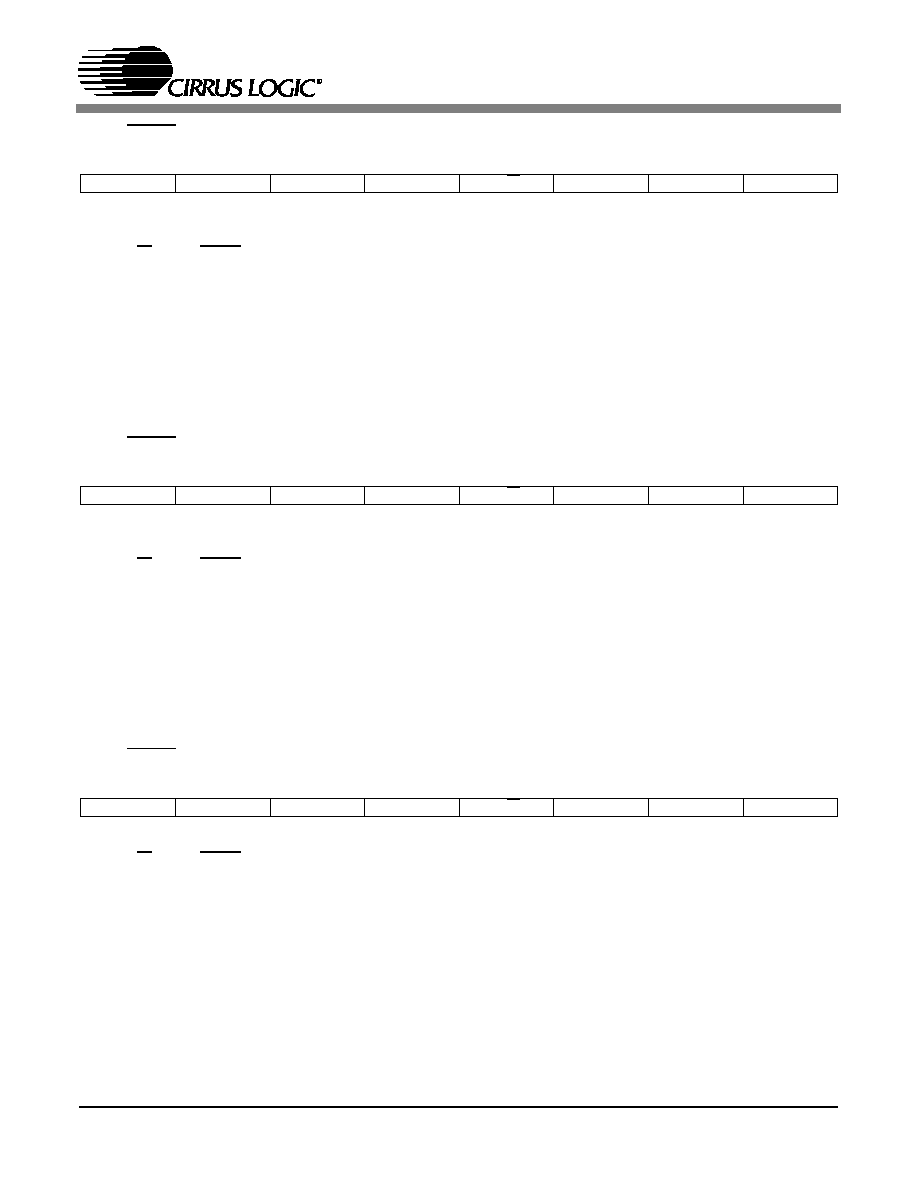
Reserved
System-Offset Calibration
System-Gain Calibration
Reserved
CS5531/32/33/34
20
DS289PP5
2.2.3. Command Register Descriptions
READ/WRITE ALL OFFSET CALIBRATION REGISTERS
Function:
These commands are used to access the offset registers as arrays.
R/W (Read/Write)
0
Write to selected registers.
1
Read from selected registers.
READ/WRITE ALL GAIN CALIBRATION REGISTERS
Function:
These commands are used to access the gain registers as arrays.
R/W (Read/Write)
0
Write to selected registers.
1
Read from selected registers.
READ/WRITE ALL CHANNEL-SETUP REGISTERS
Function:
These commands are used to access the channel-setup registers as arrays.
R/W (Read/Write)
0
Write to selected registers.
1
Read from selected registers.
READ/WRITE INDIVIDUAL OFFSET REGISTER
Function
:
These commands are used to access each offset register separately. CS1 - CS0 decode the
registers accessed.
R/W (Read/Write)
0
Write to selected register.
1
Read from selected register.
CS[1:0] (Channel Select Bits)
00
Offset Register 1 (All devices)
01
Offset Register 2 (All devices)
10
Offset Register 3 (CS5533/34 only)
11
Offset Register 4 (CS5533/34 only)
D7(MSB)
D6
D5
D4
D3
D2
D1
D0
0
1
0
0
R/W
0
0
1
D7(MSB)
D6
D5
D4
D3
D2
D1
D0
0
1
0
0
R/W
0
1
0
D7(MSB)
D6
D5
D4
D3
D2
D1
D0
0
1
0
0
R/W
1
0
1
D7(MSB)
D6
D5
D4
D3
D2
D1
D0
0
0
CS1
CS0
R/W
0
0
1
CS5531/32/33/34
DS289PP5
21
READ/WRITE INDIVIDUAL GAIN REGISTER
Function
:
These commands are used to access each gain register separately. CS1 - CS0 decode the reg-
isters accessed.
R/W (Read/Write)
0
Write to selected register.
1
Read from selected register.
CS[1:0] (Channel Select Bits)
00
Gain Register 1 (All devices)
01
Gain Register 2 (All devices)
10
Gain Register 3 (CS5533/34 only)
11
Gain Register 4 (CS5533/34 only)
READ/WRITE INDIVIDUAL CHANNEL-SETUP REGISTER
Function
:
These commands are used to access each channel-setup register separately. CS1 - CS0 de-
code the registers accessed.
R/W (Read/Write)
0
Write to selected register.
1
Read from selected register.
CS[1:0] (Channel Select Bits)
00
Channel-Setup Register 1 (All devices)
01
Channel-Setup Register 2 (All devices)
10
Channel-Setup Register 3 (All devices)
11
Channel-Setup Register 4 (All devices)
READ/WRITE CONFIGURATION REGISTER
Function:
These commands are used to read from or write to the configuration register.
R/W (Read/Write)
0
Write to selected register.
1
Read from selected register.
D7(MSB)
D6
D5
D4
D3
D2
D1
D0
0
0
CS1
CS0
R/W
0
1
0
D7(MSB)
D6
D5
D4
D3
D2
D1
D0
0
0
CS1
CS0
R/W
1
0
1
D7(MSB)
D6
D5
D4
D3
D2
D1
D0
0
0
0
0
R/W
0
1
1

CS5531/32/33/34
22
DS289PP5
PERFORM CONVERSION
Function:
These commands instruct the ADC to perform either a single, fully-settled conversion or con-
tinuous conversions on the physical input channel pointed to by the pointer bits (CSRP2 -
CRSP0) in the channel-setup register.
MC (Multiple Conversions)
0
Perform a single conversion.
1
Perform continuous conversions.
CSRP [2:0] (Channel Setup Register Pointer Bits)
000
Setup 1 (All devices)
001
Setup 2 (All devices)
010
Setup 3 (All devices)
011
Setup 4 (All devices)
100
Setup 5 (All devices)
101
Setup 6 (All devices)
110
Setup 7 (All devices)
111
Setup 8 (All devices)
D7(MSB)
D6
D5
D4
D3
D2
D1
D0
1
MC
CSRP2
CSRP1
CSRP0
0
0
0

CS5531/32/33/34
DS289PP5
23
PERFORM CALIBRATION
Function:
These commands instruct the ADC to perform a calibration on the physical input channel se-
lected by the setup register which is chosen by the command byte pointer bits (CSRP2 -
CSRP0).
CSRP [2:0] (Channel Setup Register Pointer Bits)
000
Setup 1 (All devices)
001
Setup 2 (All devices)
010
Setup 3 (All devices)
011
Setup 4 (All devices)
100
Setup 5 (All devices)
101
Setup 6 (All devices)
110
Setup 7 (All devices)
111
Setup 8 (All devices)
CC [2:0] (Calibration Control Bits)
000
Reserved
001
Self-Offset Calibration
010
Self-Gain Calibration
011
Reserved
100
Reserved
101
System-Offset Calibration
110
System-Gain Calibration
111
Reserved
SYNC1
Function:
Part of the serial port re-initialization sequence.
SYNC0
Function:
End of the serial port re-initialization sequence.
NULL
Function:
This command is used to clear a port flag and keep the converter in the continuous conversion mode.
D7(MSB)
D6
D5
D4
D3
D2
D1
D0
1
0
CSRP2
CSRP1
CSRP0
CC2
CC1
CC0
D7(MSB)
D6
D5
D4
D3
D2
D1
D0
1
1
1
1
1
1
1
1
D7(MSB)
D6
D5
D4
D3
D2
D1
D0
1
1
1
1
1
1
1
0
D7(MSB)
D6
D5
D4
D3
D2
D1
D0
0
0
0
0
0
0
0
0

CS5531/32/33/34
24
DS289PP5
2.2.4. Serial Port Interface
The CS5531/32/33/34's serial interface consists of
four control lines: CS, SDI, SDO, SCLK. Figure 7
details the command and data word timing.
CS, Chip Select, is the control line which enables
access to the serial port. If the CS pin is tied low,
the port can function as a three wire interface.
SDI, Serial Data In, is the data signal used to trans-
fer data to the converters.
SDO, Serial Data Out, is the data signal used to
transfer output data from the converters. The SDO
output will be held at high impedance any time CS
is at logic 1.
SCLK, Serial Clock, is the serial bit-clock which
controls the shifting of data to or from the ADC's
serial port. The CS pin must be held low (logic 0)
before SCLK transitions can be recognized by the
port logic. To accommodate optoisolators SCLK is
designed with a Schmitt-trigger input to allow an
optoisolator with slower rise and fall times to di-
rectly drive the pin. Additionally, SDO is capable
of sinking or sourcing up to 5 mA to directly drive
an optoisolator LED. SDO will have less than a 400
mV loss in the drive voltage when sinking or sourc-
ing 5 mA.
Command Time
8 SCLKs
Data Time 32 SCLKs
Write Cycle
CS
SCLK
SDI
MSB
Command Time
8 SCLKs
CS
SCLK
SDI
Read Cycle
SDO
MSB
LSB
Command Time
8 SCLKs
8 SCLKs Clear SDO Flag
SDO
SCLK
SDI
MSB
LSB
Clock Cycles
t *
d
CS
00
00
00
00
00
00
00
00
00
00
00
00
00
00
00
00
00
00
00
00
00
00
00
00
00
00
00
00
00
00
00
00
00
00
00
00
00
00
00
00
00
00
00
00
00
00
00
00
00
00
00
00
00
00
00
00
00
00
00
00
00
00
00
00
00
00
00
00
00
00
00
00
00
00
00
000
000
000
000
000
000
000
000
000
000
000
000
000
000
000
000
000
000
000
000
000
000
000
000
000
000
000
000
000
000
000
000
000
000
000
000
000
000
000
000
000
000
000
000
Data Time 32 SCLKs
Data Time 32 SCLKs
LSB
Data Conversion Cycle
/OWR
MCLK
* td is the time it takes the ADC to perform a conversion. See the Single
Conversion and Continuous Conversion sections of the data sheet for more
details about conversion timing.
Figure 7. Command and Data Word Timing

CS5531/32/33/34
DS289PP5
25
2.2.5. Reading/Writing On-Chip Registers
The CS5531/32/33/34's offset, gain, configuration,
and channel-setup registers are readable and writ-
able while the conversion data register is read only.
As shown in Figure 7, to write to a particular regis-
ter the user must transmit the appropriate write
command and then follow that command by 32 bits
of data. For example, to write 0x80000000 (hexa-
decimal) to physical channel one's gain register,
the user would first transmit the command byte
0x02
(hexadecimal)
followed
by
the
data
0x80000000 (hexadecimal). Similarly, to read a
particular register the user must transmit the appro-
priate read command and then acquire the 32 bits of
data. Once a register is written to or read from, the
serial port returns to the command mode.
In addition to accessing the internal registers one at
a time, the gain and offset registers as well as the
channel setup registers can be accessed as arrays
(i.e. the entire register set can be accessed with one
command). In the CS5531/32, there are two gain
and offset registers, and in the CS5533/34, there are
four gain and offset registers. There are four chan-
nel setup registers in all parts. As an example, to
write 0x80000000 (hexadecimal) to all four gain
registers in the CS5533, the user would transmit the
command 0x42 (hexadecimal) followed by four it-
erations of 0x80000000 (hexadecimal), (i.e. 0x42
followed
by
0x80000000,
0x80000000,
0x80000000, 0x80000000). The registers are writ-
ten to or read from in sequential order (i.e, 1, fol-
lowed by 2, 3, and 4). Once the registers are written
to or read from, the serial port returns to the com-
mand mode.
2.3. Configuration Register
To ease the architectural design and simplify the
serial interface, the configuration register is thirty-
two bits long, however, only eleven of the thirty
two bits are used. The following sections detail the
bits in the configuration register.
2.3.1. Power Consumption
The CS5531/32/33/34 accommodate three power
consumption modes: normal, standby, and sleep.
The default mode, "normal mode", is entered after
power
is
applied.
In
this
mode,
the
CS5531/32/33/34-AS versions typically consume
35 mW. The CS5532/34-BS versions typically
consume 70 mW. The other two modes are referred
to as the power save modes. They power down
most of the analog portion of the chip and stop filter
convolutions. The power save modes are entered
whenever the power down (PDW) bit of the config-
uration register is set to logic 1. The particular pow-
er save mode entered depends on state of the PSS
(Power Save Select) bit. If PSS is logic 0, the con-
verter enters the standby mode reducing the power
consumption to 4 mW. The standby mode leaves
the oscillator and the on-chip bias generator for the
analog portion of the chip active. This allows the
converter to quickly return to the normal mode
once PDW is set back to a logic 1. If PSS and PDW
are both set to logic 1, the sleep mode is entered re-
ducing the consumed power to around 500
µ
W.
Since this sleep mode disables the oscillator, ap-
proximately a 20 ms oscillator start-up delay period
is required before returning to the normal mode. If
an external clock is used, there will be no delay.
Further note that when the chips are used in the
Gain = 1 mode, the PGIA is powered down. With
the PGIA powered down, the power consumed in
the normal power mode is reduced by approximate-
ly 1/2. Power consumption in the sleep and standby
modes is not affected by the amplifier setting.
2.3.2. System Reset Sequence
The reset system (RS) bit permits the user to per-
form a system reset. A system reset can be initiated
at any time by writing a logic 1 to the RS bit in the
configuration register. After the RS bit has been
set, the internal logic of the chip will be initialized
to a reset state. The reset valid (RV) bit is set indi-
cating that the internal logic was properly reset.

CS5531/32/33/34
26
DS289PP5
The RV bit is cleared after the configuration regis-
ter is read. The on-chip registers are initialized to
the following default states:
After reset, the RS bit should be written back to
logic 0 to complete the reset cycle. The ADC will
return to the command mode where it waits for a
valid command. Also, the RS bit is the only bit in
the configuration register that can be set when ini-
tiating a reset (i.e. a second write command is need-
ed to set other bits in the Configuration Register
after the RS bit has been cleared).
2.3.3. Input Short
The input short bit allows the user to internally
ground all the inputs of the multiplexer. This is a
useful function because it allows the user to easily
test the grounded input performance of the ADC
and eliminate the noise effects due to the external
system components.
2.3.4. Guard Signal
The guard signal bit is a bit that modifies the func-
tion of A0. When set, this bit outputs the common
mode voltage of the instrumentation amplifier on
A0. This feature is useful when the user wants to
connect an external shield to the common mode po-
tential of the instrumentation amplifier to protect
against leakage. Figure 8 illustrates a typical con-
nection diagram for the guard signal.
2.3.5. Voltage Reference Select
The voltage reference select (VRS) bit selects the
size of the sampling capacitor used to sample the
voltage reference. The bit should be set based upon
the magnitude of the reference voltage to achieve
optimal performance. Figures 9 and 10 model the
effects on the reference's input impedance and in-
put current for each VRS setting. As the models
show, the reference includes a coarse/fine charge
buffer which reduces the dynamic current demand
of the external reference.
The reference's input buffer is designed to accom-
modate rail-to-rail (common-mode plus signal) in-
put voltages. The differential voltage between the
VREF+ and VREF- can be any voltage from 1.0 V
up to the analog supply (depending on how VRS is
configured), however, the VREF+ cannot go above
VA+ and the VREF- pin can not go below VA-.
Note that the power supplies to the chip should be
established before the reference voltage.
2.3.6. Output Latch Pins
The A1-A0 pins of the ADCs mimic the D21-
D20/D5-D4 bits of the channel-setup registers if
the output latch select (OLS) bit is logic 0 (default).
If the OLS bit is logic 1, A1-A0 mimic the output
latch bit settings in the configuration register.
These two options give the user a choice of allow-
ing the latch outputs to change anytime a different
CSR is selected for a conversion, or to allow the
latch bits to remain latched to a fixed state (deter-
mined by the configuration register bit) for all CSR
selections. In either case, A1-A0 can be used to
control external multiplexers and other logic func-
tions outside the converter. The A1-A0 outputs can
sink or source at least 1 mA, but it is recommended
Configuration Register:
00000000(H)
Offset Registers:
00000000(H)
Gain Registers:
01000000(H)
Channel Setup Registers: 00000000(H)
C o m m o n M o d e = 2 .5 V
o u t m
c e n te r
o u t p
x1
+ 5 V A +
V
+
IN
V
-
IN
C S 5 5 3 1 /3 2 /3 3 /3 4
A IN +
A IN -
A 0 /G U A R D
Figure 8. Guard Signal Shielding Scheme
CS5531/32/33/34
DS289PP5
27
to limit drive currents to less than 20
µ
A to reduce
self-heating of the chip. These outputs are powered
from VA+ and VA-. Their output voltage will be
limited to the VA+ voltage for a logic 1 and VA-
for a logic 0.
2.3.7. Offset and Gain Select
The Offset and Gain Select bit (OGS) is used to se-
lect the source of the calibration registers to use
when performing conversions and calibrations.
When the OGS bit is set to `0', the offset and gain
registers corresponding to the desired physical
channel (CS1-CS0 in the selected Setup) will be ac-
cessed. When the OGS bit is set to `1', the offset
and gain registers pointed to by the OG1-OG0 bits
in the selected Setup will be accessed. This feature
allows multiple calibration values (e.g. for different
gain settings) to be used on a single physical chan-
nel without having to re-calibrate or manipulate the
calibration registers.
2.3.8. Filter Rate Select
The Filter Rate Select bit (FRS) modifies the output
word rates of the converter to allow either 50 Hz or
60 Hz rejection when operating from a 4.9152
MHz crystal. If FRS is cleared to logic 0, the word
rates and corresponding filter characteristics can be
selected (using the Channel Setup Registers) from
7.5, 15, 30, 60, 120, 240, 480, 960, 1920, or 3840
Sps when using a 4.9152 MHz clock. If FRS is set
to logic 1, the word rates and corresponding filter
characteristics scale by a factor of 5/6, making the
selectable word rates 6.25, 12.5, 25, 50, 100, 200,
400, 800, 1600, and 3200 Sps when using a 4.9152
MHz clock. When using other clock frequencies,
these selectable word rates will scale linearly with
the clock frequency that is used.
V R E F
C = 22 p F
f =
2
F in e
1
V
1 5 m V
i = fV
C
os
os
n
C o a rs e
MCLK
16
VRS = 1; 1 V
V
2.5 V
REF
Figure 9. Input Reference Model when VRS = 1
V R E F
C = 1 1p F
f =
2
F in e
1
V
3 0 m V
i = fV
C
o s
os
n
C o a rs e
MCLK
16
VRS = 0; 2.5 V < V
VA+
REF
Figure 10. Input Reference Model when VRS = 0

CS5531/32/33/34
28
DS289PP5
2.3.9. Configuration Register Descriptions
PSS (Power Save Select)[31]
0
Standby Mode (Oscillator active, allows quick power-up).
1
Sleep Mode (Oscillator inactive).
PDW (Power Down Mode)[30]
0
Normal Mode
1
Activate the power save select mode.
RS (Reset System)[29]
0
Normal Operation.
1
Activate a Reset cycle. See System Reset Sequence in the datasheet text.
RV (Reset Valid)[28]
0
Normal Operation
1
System was reset. This bit is read only. Bit is cleared to logic zero after the configuration register is read.
IS (Input Short)[27]
0
Normal Input
1
All signal input pairs for each channel are disconnected from the pins and shorted internally.
GB (Guard Signal Bit)[26]
0
Normal Operation of A0 as an output latch.
1
A0's output is modified to output the common mode output voltage of the instrumentation amplifier (typically
2.5 V). The output latch select bit is ignored when the guard buffer is activated.
VRS (Voltage Reference Select)[25]
0
2.5 V < V
REF
[(VA+) - (VA-)]
1
1 V
V
REF
2.5V
A1-A0 (Output Latch bits)[24:23]
The latch bits (A0 and A1) will be set to the logic state of these bits upon command word execution if the output
latch select bit (OLS) is set. Note that these logic outputs are powered from VA+ and VA-.
00
A0 = 0, A1 = 0
01
A0 = 0, A1 = 1
10
A0 = 1, A1 = 0
11
A0 = 1, A1 = 1
Output Latch Select, OLS[22]
0
When low, uses the Channel-Setup Register as the source of A1 and A0.
1
When set, uses the Configuration Register as the source of A1 and A0.
NU (Not Used)[21]
0
Must always be logic 0. Reserved for future upgrades.
Offset and Gain Select OGS[20]
0
Calibration registers used are based on the CS1-CS0 bits of the referenced Setup.
1
Calibration registers used are based on the OG1-OG0 bits of the referenced Setup.
D31(MSB)
D30
D29
D28
D27
D26
D25
D24
D23
D22
D21
D20
D19
D18
D17
D16
PSS
PDW
RS
RV
IS
GB
VRS
A1
A0
OLS
NU
OGS
FRS
NU
NU
NU
D15
D14
D13
D12
D11
D10
D9
D8
D7
D6
D5
D4
D3
D2
D1
D0
NU
NU
NU
NU
NU
NU
NU
NU
NU
NU
NU
NU
NU
NU
NU
NU

CS5531/32/33/34
DS289PP5
29
Filter Rate Select, FRS[19]
0
Use the default output word rates.
1
Scale all output word rates and their corresponding filter characteristics by a factor of 5/6.
NU (Not Used)[18:0]
0
Must always be logic 0. Reserved for future upgrades.
2.4. Setting up the CSRs for a Measurement
The CS5531/32/33/34 have four Channel-Setup
Registers (CSRs). Each CSR contains two 16-bit
Setups which are programmed by the user to contain
data conversion information such as: 1) which phys-
ical channel will be converted, 2) at what gain will
the channel be converted, 3) at what word rate will
the channel be converted, 4) will the output conver-
sion be unipolar or bipolar, 5) what will be the state
of the output latch during the conversion, 6) will the
converter delay the start of a conversion to allow
time for the output latch to settle before the conver-
sion is begun, and 7) will the open circuit detect cur-
rent source be activated for that Setup. In addition,
when the OGS bit in the Configuration Register is
set, the Setup selects which set of offset and gain
registers to use when performing conversions or cal-
ibrations. Note that a particular physical input chan-
nel can be represented in more than one Setup with
different output rates, gain ranges, etc. (i.e. each
Setup is independently defined). Refer to section
2.4.1 for more details about the Channel Setup
Registers.
Each 32-bit CSR is individually accessible and
contains two 16-bit Setups. As an example, to con-
figure Setup 1 in the CS5531/32/33/34 with the
write individual channel-setup register command
(0x05 hexadecimal), bits 31 to 16 of CSR 1 con-
tains the information for Setup 1 and bits 15 to 0
contain the information for Setup 2. Note that while
reading/writing CSRs, two Setups are accessed in
pairs as a single 32-bit CSR register. Even if one of
the Setups isn't used, it must be written to or read.
Examples detailing the power of the CSRs are pro-
vided in section 2.6.3.

CS5531/32/33/34
30
DS289PP5
2.4.1. Channel-Setup Register Descriptions
CS1-CS0 (Channel Select Bits) [31:30] [15:14]
00
Select physical channel 1 (All devices)
01
Select physical channel 2 (All devices)
10
Select physical channel 3 (CS5533/34 only)
11
Select physical channel 4 (CS5533/34 only)
G2-G0 (Gain Bits) [29:27] [13:11]
For VRS = 0, A = 2; For VRS = 1, A = 1; Bipolar input span is twice the unipolar input span.
000
Gain = 1, (Input Span = [(VREF+)-(VREF-)]/1*A for unipolar).
001
Gain = 2, (Input Span = [(VREF+)-(VREF-)]/2*A for unipolar).
010
Gain = 4, (Input Span = [(VREF+)-(VREF-)]/4*A for unipolar).
011
Gain = 8, (Input Span = [(VREF+)-(VREF-)]/8*A for unipolar).
100
Gain = 16, (Input Span = [(VREF+)-(VREF-)]/16*A for unipolar).
101
Gain = 32, (Input Span = [(VREF+)-(VREF-)]/32*A for unipolar).
110
Gain = 64, (Input Span = [(VREF+)-(VREF-)]/64*A for unipolar).
WR3-WR0 (Word Rate) [26:23] [10:7]
The listed Word Rates are for continuous conversion mode using a 4.9152 MHz clock. All word rates will
scale linearly with the clock frequency used. The very first conversion using continuous conversion mode
will last longer, as will conversions done with the single conversion mode. See the section on Performing
Conversions and Tables 1 and 2 for more details.
Bit
WR (FRS = 0)
WR (FRS = 1)
0000
120 Sps
100 Sps
0001
60 Sps
50 Sps
0010
30 Sps
25 Sps
0011
15 Sps
12.5 Sps
0100
7.5 Sps
6.25 Sps
1000
3840 Sps
3200 Sps
1001
1920 Sps
1600 Sps
1010
960 Sps
800 Sps
1011
480 Sps
400 Sps
1100
240 Sps
200 Sps
All other combinations are not used.
D31(MSB)
D30
D29
D28
D27
D26
D25
D24
D23
D22
D21
D20
D19
D18
D17
D16
CS1
CS0
G2
G1
G0
WR3
WR2
WR1
WR0
U/B
OL1
OL0
DT
OCD
OG1
OG0
D15
D14
D13
D12
D11
D10
D9
D8
D7
D6
D5
D4
D3
D2
D1
D0
CS1
CS0
G2
G1
G0
WR3
WR2
WR1
WR0
U/B
OL1
OL0
DT
OCD
OG1
OG0
CSR
#1
Setup 1
Bits <127:112>
Setup 2
Bits <111:96>
#4
Setup 7
Bits <31:16>
Setup 8
Bits <15:0>

CS5531/32/33/34
DS289PP5
31
U/B (Unipolar / Bipolar) [22] [6]
0
Select Bipolar mode.
1
Select Unipolar mode.
OL1-OL0 (Output Latch Bits) [21:20] [5:4]
The latch bits will be set to the logic state of these bits upon command word execution when the output
latch select bit (OLS) in the configuration register is logic 0. Note that the logic outputs on the chip are
powered from VA+ and VA-.
00
A0 = 0, A1 = 0
01
A0 = 0, A1 = 1
10
A0 = 1, A1 = 0
11
A0 = 1, A1 = 1
DT (Delay Time Bit) [19] [3]
When set, the converter will wait for a delay time before starting a conversion. This allows settling time for
A0 and A1 outputs before a conversion begins. The delay time will be 1280 MCLK cycles when FRS = 0,
and 1536 MCLK cycles when FRS = 1.
0
Begin Conversions Immediately.
1
Wait 1280 MCLK cycles (FRS = 0) or 1536 MCLK cycles (FRS = 1) before starting conversion.
OCD (Open Circuit Detect Bit) [18] [2]
When set, this bit activates a 300 nA current source on the input channel (AIN+) selected by the channel
select bits. Note that the 300nA current source is rated at 25°C. At -55°C, the current source doubles to
approximately 600nA. This feature is particularly useful in thermocouple applications when the user wants
to drive a suspected open thermocouple lead to a supply rail.
0
Normal mode.
1
Activate current source.
OG1-OG0 (Offset / Gain Register Pointer Bits) [17:16] [1:0]
These bits are only used when OGS in the Configuration Register is set to `1'. They allow the user to select
the offset and gain register to use while performing a conversion or calibration. When the OGS bit in the
Configuration Register is set to `0', the offset and gain register for the referenced physical channel (CS1-
CS0 bits of the Setup) will be used.
00
Use offset and gain register from physical channel 1
01
Use offset and gain register from physical channel 2
10
Use offset and gain register from physical channel 3
11
Use offset and gain register from physical channel 4

CS5531/32/33/34
32
DS289PP5
2.5. Calibration
Calibration is used to set the zero and gain slope of
the ADC's transfer function. The CS5531/32/33/34
offer both self calibration and system calibration.
Note:
After the ADCs are reset, they are functional
and can perform measurements without
being calibrated (remember that the VRS bit
in the configuration register must be properly
configured). In this case, the converter will
utilize the initialized values of the on-chip
registers (Gain = 1.0, Offset = 0.0) to
calculate output words. Any initial offset and
gain errors in the internal circuitry of the chip
will remain.
2.5.1. Calibration Registers
The CS5531/32/33/34 converters have an individu-
al offset and gain register for each channel input.
The gain and offset registers, which are used during
both self and system calibration, are used to set the
zero and gain slope of the converter's transfer func-
tion. As shown in Offset Register section, one LSB
in the offset register is 1.83007966 X 2
-24
propor-
tion of the input span (bipolar span is 2 times the
unipolar span, gain register = 1.000...000 decimal).
The MSB in the offset register determines if the
offset to be trimmed is positive or negative (0 pos-
itive, 1 negative). Note that the magnitude of the
offset that is trimmed from the input is mapped
through the gain register. The converter can typi-
cally trim ±100 percent of the input span. As shown
in the Gain Register section, the gain register spans
from 0 to (64 - 2
-24
). The decimal equivalent mean-
ing of the gain register is
where the binary numbers have a value of either
zero or one (b
D29
is the binary value of bit D29).
While gain register settings of up to 64 - 2
-24
are
available, the gain register should never be set to
values above 40.
2.5.2. Gain Register
The gain register span is from 0 to (64-2
-24
). After Reset D24 is 1, all other bits are `0'.
2.5.3. Offset Register
One LSB represents 1.83007966 X 2
-24
proportion of the input span (bipolar span is 2 times unipolar span).
Offset and data word bits align by MSB. After reset, all bits are `0'.
The offset register is stored as a 32-bit, two's complement number, where the last 8 bits are all 0.
D
b
D 29
2
5
b
D28
2
4
b
D 27
2
3
...
b
D0
2
24
)
+
+
+
+
b
Di
2
24
i
+
(
)
i
0
=
29
=
=
MSB
D30
D29
D28
D27
D26
D25
D24
D23
D22
D21
D20
D19
D18
D17
D16
NU
NU
2
5
2
4
2
3
2
2
2
1
2
0
2
-1
2
-2
2
-3
2
-4
2
-5
2
-6
2
-7
2
-8
0
0
0
0
0
0
0
1
0
0
0
0
0
0
0
0
D15
D14
D13
D12
D11
D10
D9
D8
D7
D6
D5
D4
D3
D2
D1
LSB
2
-9
2
-10
2
-11
2
-12
2
-13
2
-14
2
-15
2
-16
2
-17
2
-18
2
-19
2
-20
2
-21
2
22
2
-23
2
-24
0
0
0
0
0
0
0
0
0
0
0
0
0
0
0
0
MSB
D30
D29
D28
D27
D26
D25
D24
D23
D22
D21
D20
D19
D18
D17
D16
Sign
2
-2
2
-3
2
-4
2
-5
2
-6
2
-7
2
-8
2
-9
2
-10
2
-11
2
-12
2
-13
2
-14
2
-15
2
-16
0
0
0
0
0
0
0
0
0
0
0
0
0
0
0
0
D15
D14
D13
D12
D11
D10
D9
D8
D7
D6
D5
D4
D3
D2
D1
LSB
2
-17
2
-18
2
-19
2
-20
2
-21
2
-22
2
-23
2
-24
NU
NU
NU
NU
NU
NU
NU
NU
0
0
0
0
0
0
0
0
0
0
0
0
0
0
0
0

CS5531/32/33/34
DS289PP5
33
2.5.4. Performing Calibrations
To perform a calibration, the user must send a com-
mand byte with its MSB=1, its pointer bits
(CSRP2-CSRP0) set to address the desired Setup to
calibrate, and the appropriate calibration bits (CC2-
CC0) set to choose the type of calibration to be per-
formed. Note that calibration assumes that the
CSRs have been previously initialized because the
information concerning the physical channel, its
filter rate, gain range, and polarity, comes from the
channel-setup register addressed by the pointer bits
in the command byte. Once the CSRs are initial-
ized, a calibration can be performed with one com-
mand byte.
The length of time it takes to do a calibration is
slightly less than the amount of time it takes to do
a single conversion (see Table 1 for single conver-
sion timing). Offset calibration takes 608 clock cy-
cles less than a single conversion when FRS = 0,
and 729 clock cycles less when FRS = 1. Gain cal-
ibration takes 128 clock cycles less than a single
conversion when FRS = 0, and 153 clock cycles
less when FRS = 1.
Once a calibration cycle is complete, SDO falls and
the results are automatically stored in either the
gain or offset register for the physical channel be-
ing calibrated when the OGS bit in the Configura-
tion Register is set to `0'. If the OGS bit is set to `1',
the results will be stored in the register specified by
the OG1-OG0 bits of the selected Setup. See the
OGS bit description for more details (Section
2.3.7). SDO will remain low until the next com-
mand word is begun. If additional calibrations are
performed while referencing the same calibration
registers, the last calibration results will replace the
effects from the previous calibration as only one
offset and gain register is available per physical
channel. Only one calibration is performed with
each command byte. To calibrate all the channels,
additional calibration commands are necessary.
2.5.5. Self Calibration
The CS5531/32/33/34 offer both self offset and self
gain calibrations. For the self-calibration of offset,
the converters internally tie the inputs of the 1X
amplifier together and routes them to the AIN- pin
as shown in Figure 11. For accurate self-calibration
of offset to occur, the AIN pins must be at the prop-
er common-mode-voltage as specified in the Analog
Characteristics section. Self offset calibration uses
the 1X gain amplifier, and is therefore not valid in
the 2X-64X gain ranges. A self offset calibration of
these gain ranges can be performed by setting the IS
bit in the configuration register to a `1', and perform-
ing a system offset calibration. The IS bit must be re-
turned to `0' afterwards for normal operation of the
device.
For self-calibration of gain, the differential inputs
of the modulator are connected to VREF+ and
VREF- as shown in Figure 12. Self-calibration of
gain will not work with (VREF+ - VREF-) > 2.5V.
Self-calibration of gain is performed in the GAIN =
1x mode without regard to the setup register's gain
setting. Gain errors in the PGIA gain steps 2x to
64x are not calibrated as this would require an ac-
curate low voltage source other than the reference
voltage. A system calibration of gain should be per-
formed if accurate gains are to be achieved on the
ranges other than 1X, or when (VREF+ - VREF-) >
2.5V.

CS5531/32/33/34
34
DS289PP5
2.5.6. System Calibration
For the system calibration functions, the user must
supply the converters calibration signals which repre-
sent ground and full scale. When a system offset cal-
ibration is performed, a ground referenced signal
must be applied to the converters. Figure 13 illus-
trates system offset calibration.
As shown in Figure 14, the user must input a signal
representing the positive full scale point to perform
a system gain calibration. In either case, the cali-
bration signals must be within the specified calibra-
tion limits for each specific calibration step (refer
to the System Calibration Specifications).
2.5.7. Calibration Tips
Calibration steps are performed at the output word
rate selected by the WR2-WR0 bits of the channel
setup registers. Due to limited register lengths in
the faster word-rate filters (240 Sps and higher),
channels that are used in these rates should also be
calibrated in one of these word rates, and channels
used in the lower word rates (120 Sps and lower)
should be calibrated at one of these lower rates.
Since higher word rates result in conversion words
with more peak-to-peak noise, calibration should
be performed at the lowest possible output word
rate for maximum accuracy. For the 7.5 Sps to 120
Sps word rate settings, calibrations can be per-
formed at 7.5 Sps, and for 240 Sps and higher, cal-
ibration can be performed at 240 Sps. To minimize
digital noise near the device, the user should wait
for each calibration step to be completed before
reading or writing to the serial port. Reading the
calibration registers and averaging multiple cali-
brations together can produce a more accurate cal-
ibration result. Note that accessing the ADC's
serial port before a calibration has finished may re-
AIN+
AIN-
S1
OPE N
S2
C LO SED
+
-
1X G AIN
+
-
Figure 11. Self Calibration of Offset
AIN+
AIN-
OPEN
+
-
XGAIN
+
-
OPEN
CLOSED
VREF+
CLOSED
VREF-
+
-
Reference
Figure 12. Self Calibration of Gain
+
-
XGAIN
+
-
External
Connections
0V
+
-
AIN+
AIN-
CM +
-
Figure 13. System Calibration of Offset
+
-
XGAIN
+
-
External
Connections
Full Scale +
-
AIN+
AIN-
CM +
-
Figure 14. System Calibration of Gain

CS5531/32/33/34
DS289PP5
35
sult in the loss of synchronization between the mi-
crocontroller and the ADC, and may prematurely
halt the calibration cycle.
For maximum accuracy, calibrations should be per-
formed for both offset and gain (selected by chang-
ing the G2-G0 bits of the channel-setup registers).
Note that only one gain range can be calibrated per
physical channel when the OGS bit in the Configu-
ration Register is set to `0'. Multiple gain ranges
can be calibrated for a single channel by manipulat-
ing the OGS bit and the OG1-OG0 bits of the se-
lected Setup (see Section 2.3.7 for more details). If
factory calibration of the user's system is per-
formed using the system calibration capabilities of
the CS5531/32/33/34, the offset and gain register
contents can be read by the system microcontroller
and recorded in non-volatile memory. These same
calibration words can then be uploaded into the off-
set and gain registers of the converter when power
is first applied to the system, or when the gain range
is changed.
When the device is used without calibration, the
uncalibrated gain accuracy is about ±1 percent and
the gain tracking from range (2X to 64X) to range
is approximately ±0.3 percent.
Note that the gain from the offset register to the
output is 1.83007966 decimal, not 1. If a user wants
to adjust the calibration coefficients externally,
they will need to divide the information to be writ-
ten to the offset register by the scale factor of
1.83007966. (This discussion assumes that the gain
register is 1.000...000 decimal. The offset register
is also multiplied by the gain register before being
applied to the output conversion words).
2.5.8. Limitations in Calibration Range
System calibration can be limited by signal head-
room in the analog signal path inside the chip as
discussed under the Analog Input section of this
data sheet. For gain calibration, the full scale input
signal can be reduced to 3% of the nominal full-
scale value. At this point, the gain register is ap-
proximately equal to 33.33 (decimal). While the
gain register can hold numbers all the way up to 64
- 2
-24
, gain register settings above a decimal value
of 40 should not be used. With the converter's in-
trinsic gain error, this minimum full scale input sig-
nal may be higher or lower. In defining the
minimum Full Scale Calibration Range (FSCR)
under Analog Characteristics, margin is retained to
accommodate the intrinsic gain error. Inversely, the
input full scale signal can be increased to a point in
which the modulator reaches its 1's density limit of
86 percent, which under nominal conditions occurs
when the full scale input signal is 1.1 times the
nominal full scale value. With the chip's intrinsic
gain error, this maximum full scale input signal
maybe higher or lower. In defining the maximum
FSCR, margin is again incorporated to accommo-
date the intrinsic gain error.
2.6. Performing Conversions
The CS5531/32/33/34 offers two distinctly differ-
ent conversion modes. The three sections that fol-
low detail the differences and provide examples
illustrating how to use the conversion modes with
the channel-setup registers.
2.6.1. Single Conversion Mode
Based on the information provided in the channel-
setup registers (CSRs), after the user transmits the
conversion command, a single, fully-settled con-
version is performed. The command byte includes
a pointer address to the Setup register to be used
during the conversion. Once transmitted, the serial
port enters data mode where it waits until the con-
version is complete. When the conversion data is
available, SDO falls to logic 0. Forty SCLKs are
then needed to read the conversion data word. The
first 8 SCLKs are used to clear the SDO flag. Dur-
ing the first 8 SCLKs, SDI must be logic 0. The last
32 SCLKs are needed to read the conversion result.
Note that the user is forced to read the conversion
in single conversion mode as SDO will remain low

CS5531/32/33/34
36
DS289PP5
(i.e. the serial port is in data mode) until SCLK
transitions 40 times. After reading the data, the se-
rial port returns to the command mode, where it
waits for a new command to be issued. The single
conversion mode will take longer than conversions
performed in the continuous conversion mode. The
number of clock cycles a single conversion takes
for each Output Word Rate (OWR) setting is listed
in Table 1. The
±
8 (FRS = 0) or
±
10 (FRS = 1)
clock ambiguity is due to internal synchronization
between the SCLK input and the oscillator.
Note:
In the single conversion mode, more than one
conversion is actually performed, but only the
final, fully settled result is output to the
conversion data register.
Table 1. Conversion Timing for Single Mode
2.6.2. Continuous Conversion Mode
Based on the information provided in the channel-
setup registers (CSRs), continuous conversions are
performed using the Setup register contents pointed
to by the conversion command. The command byte
includes a pointer address to the Setup register to
be used during the conversion. Once transmitted,
the serial port enters data mode where it waits until
a conversion is complete. After the conversion is
done, SDO falls to logic 0. Forty SCLKs are then
needed to read the conversion. The first 8 SCLKs
are used to clear the SDO flag. The last 32 SCLKs
are needed to read the conversion result. If
`00000000' is provided to SDI during the first 8
SCLKs when the SDO flag is cleared, the converter
remains in this conversion mode and continues to
convert the selected channel using the same CSR
Setup. In continuous conversion mode, not every
conversion word needs to be read. The user needs
only to read the conversion words required for the
application as SDO rises and falls to indicate the
availability of new conversion data. Note that if a
conversion is not read before the next conversion
data becomes available, it will be lost and replaced
by the new conversion data. To exit this conversion
mode, the user must provide `11111111' to the SDI
pin during the first 8 SCLKs after SDO falls. If the
user decides to exit, 32 SCLKs are required to
clock out the last conversion before the converter
returns to command mode. The number of clock
cycles a continuous conversion takes for each Out-
put Word Setting is listed in Table 2. The first con-
version from the part in continuous conversion
mode will be longer than the following conversions
due to start-up overhead. The
±
8 (FRS = 0) or
±
10
(FRS = 1) clock ambiguity is due to internal syn-
chronization between the SCLK input and the os-
cillator.
Note:
When changing channels, or after performing
calibrations and/or single conversions, the
user must ignore the first three (for OWRs
less than 3200 Sps, MCLK = 4.9152 MHz) or
first five (for OWR
3200 Sps) conversions in
continuous conversion mode, as residual
filter coefficients must be flushed from the
filter before accurate conversions are
performed.
(WR3-WR0)
Clock Cycles
FRS = 0
FRS = 1
0000
171448 ± 8
205738 ± 10
0001
335288 ± 8
402346 ± 10
0010
662968 ± 8
795562 ± 10
0011
1318328 ± 8
1581994 ± 10
0100
2629048 ± 8
3154858 ± 10
1000
7592 ± 8
9110 ± 10
1001
17848 ± 8
21418 ± 10
1010
28088 ± 8
33706 ± 10
1011
48568 ± 8
58282 ± 10
1100
89528 ± 8
107434 ± 10
FRS (WR3-WR0)
Clock Cycles
(First Conversion)
Clock Cycles
(All Other
Conversions)
0
0000
89528 ± 8
40960
0
0001
171448 ± 8
81920
0
0010
335288 ± 8
163840
0
0011
662968 ± 8
327680
0
0100
1318328 ± 8
655360
0
1000
2472 ± 8
1280
0
1001
12728 ± 8
2560
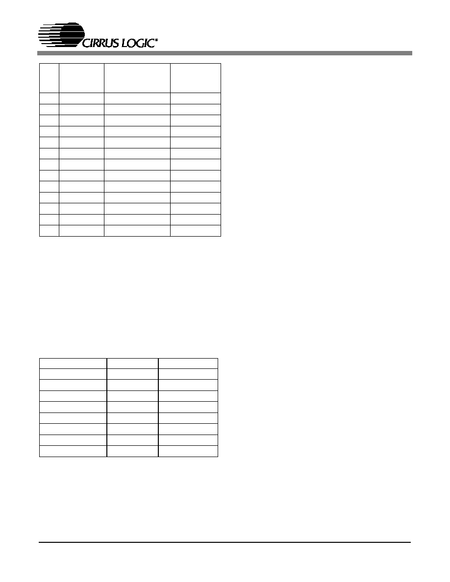
CS5531/32/33/34
DS289PP5
37
Table 2. Conversion Timing for Continuous Mode
2.6.3. Examples of Using CSRs to Perform
Conversions and Calibrations
Any time a calibration or conversion command is
issued (C, MC, and CC2-CC0 bits must be properly
set), the CSRP2-CSRP0 bits in the command byte
are used as pointers to address one of the Setups in
the channel-setup registers (CSRs). Table 3 details
the address decoding of the pointer the bits.
The examples that follow detail situations that a
user might encounter when acquiring a conversion
or calibrating the converter. These examples as-
sume that the CSRs are programmed with the fol-
lowing physical channel order: 4, 1, 1, 2, 4, 3, 4, 4.
A physical channel is defined as the actual input
channel (AIN1 to AIN4) to which an external sig-
nal is connected.
Example 1: Single conversion using Setup 1. The
command issued is `10000000'. This instructs the
converter to perform a single conversion referenc-
ing Setup 1 (CSRP2 - CSRP0 = `000') In this ex-
ample, Setup 1 points to physical channel 4. After
the command is received and decoded, the ADC
performs a conversion on physical channel 4 and
SDO falls to indicate that the conversion is com-
plete. To read the conversion, 40 SCLKs are then
required. Once the conversion data has been read,
the serial port returns to the command mode.
Example 2: Continuous conversions using Setup 3.
The command issued is `11010000'. This instructs
the converter to perform continuous conversions
referencing Setup 3 (CSRP2 - CSRP0 = `010'). In
this example, Setup 3 points to physical channel 1.
After the command is received and decoded, the
ADC performs a conversion on physical channel 1
and SDO falls to indicate that the conversion is
complete. The user now has three options. The user
can acquire the conversion and remain in this
mode, acquire the conversion and exit this mode, or
ignore the conversion and wait for a new conver-
sion at the next update interval, as detailed in the
continuous conversion section.
Example 3: Calibration using Setup 4. This exam-
ple assumes that the OGS bit in the Configuration
Register is set to `0'. The command issued is
`10011001'. This instructs the converter to perform
a self offset calibration referencing Setup 4
(CSRP2 - CSRP0 = `011'). In this example, Setup
4 points to physical channel 2. After the command
is received and decoded, the ADC performs a self
offset calibration on physical channel 2 and SDO
falls to indicate that the calibration is complete. To
perform additional calibrations, more commands
must be issued.
Note:
The CSRs need not be written. If they are not
0
1010
17848 ± 8
5120
0
1011
28088 ± 8
10240
0
1100
48568 ± 8
20480
1
0000
107434 ± 10
49152
1
0001
205738 ± 10
98304
1
0010
402346 ± 10
196608
1
0011
795562 ± 10
393216
1
0100
1581994 ± 10
786432
1
1000
2966 ± 10
1536
1
1001
15274 ± 10
3072
1
1010
21418 ± 10
6144
1
1011
33706 ± 10
12288
1
1100
58282 ± 10
24576
(CSRP2-CSRP0)
CSR Location
Setup
000
CSR #1
1
001
CSR #1
2
010
CSR #2
3
011
CSR #2
4
100
CSR #3
5
101
CSR #3
6
110
CSR#4
7
111
CSR #4
8
Table 3. Command Byte Pointer
FRS (WR3-WR0)
Clock Cycles
(First Conversion)
Clock Cycles
(All Other
Conversions)

CS5531/32/33/34
38
DS289PP5
initialized, all the Setups point to their default
settings irrespective of the conversion or
calibration mode (i.e conversions can be
performed, but only physical channel 1 will be
converted). Further note that filter
convolutions are reset (i.e. flushed) if
consecutive conversions are performed on
two different physical channels. If
consecutive conversions are performed on
the same physical channel, the filter is not
reset. This allows the ADCs to more quickly
settle full scale step inputs.
2.7. Using Multiple ADCs Synchronously
Some applications require synchronous data out-
puts from multiple ADCs converting different ana-
log channels. Multiple CS5531/32/33/34 parts can
be synchronized in a single system by using the fol-
lowing guidelines:
1) All of the ADCs in the system must be operated
from the same oscillator source.
2) All of the ADCs in the system must share com-
mon SCLK and SDI lines.
3) A software reset must be performed at the same
time for all of the ADCs after system power-up (by
selecting all of the ADCs using their respective CS
pins, and writing the reset sequence to all parts, us-
ing SDI and SCLK).
4) A start conversion command must be sent to all
of the ADCs in the system at the same time. The ±
8 clock cycles of ambiguity for the first conversion
(or for a single conversion) will be the same for all
ADCs, provided that they were all reset at the same
time.
5) Conversions can be obtained by monitoring
SDO on only one ADC, (bring CS high for all but
one part) and reading the data out of each part indi-
vidually, before the next conversion data words are
ready.
An example of a synchronous system using two
CS5532 parts is shown in Figure 15.
2.8. Conversion Output Coding
The CS5531/32/33/34 output 16-bit (CS5531/33)
and 24-bit (CS5532/34) data conversion words. To
read a conversion word the user must read the con-
version data register. The conversion data register
is 32 bits long and outputs the conversions MSB
first. The last byte of the conversion data register
contains data monitoring flags. The channel indica-
tor (CI) bits keep track of which physical channel
was converted and the overrange flag (OF) moni-
tors to determine if a valid conversion was per-
formed. Refer to the Conversion Data Output
Descriptions section for more details.
The CS5531/32/33/34 output data conversions in
binary format when operating in unipolar mode and
in two's complement when operating in bipolar
mode. Tables 4 and 5 show the code mapping for
both unipolar and bipolar mode. VFS in the tables
refers to the positive full-scale voltage range of the
converter in the specified gain range, and -VFS re-
fers to the negative full-scale voltage range of the
converter. The total differential input range (be-
tween AIN+ and AIN-) is from 0 to VFS in unipo-
lar mode, and from -VFS to VFS in bipolar mode.
CLOCK
SOURCE
CS5532
CS5532
SDO
SDI
SCLK
CS
OSC2
SDO
SDI
SCLK
CS
OSC2
µ
C
Figure 15. Synchronizing Multiple ADCs

CS5531/32/33/34
DS289PP5
39
2.8.1. Conversion Data Output Descriptions
CS5531/33 (16-BIT CONVERSIONS)
CS5532/34 (24-BIT CONVERSIONS)
Conversion Data Bits [31:16 for CS5531/33; 31:8 for CS5532/34]
These bits depict the latest output conversion.
NU (Not Used) [15:3 for CS5531/33; 7:3 for CS5532/34]
These bits are masked logic zero.
OF (Over-range Flag Bit) [2]
0
Bit is clear when over-range condition has not occurred.
1
Bit is set when input signal is more positive than the positive full scale, more negative than zero (unipolar
mode) or when the input is more negative than the negative full scale (bipolar mode).
CI (Channel Indicator Bits) [1:0]
These bits indicate which physical input channel was converted.
00
Physical Channel 1
01
Physical Channel 2
10
Physical Channel 3
11
Physical Channel 4
Unipolar Input
Voltage
Offset
Binary
Bipolar Input
Voltage
Two's
Complement
>(VFS-1.5 LSB)
FFFF
>(VFS-1.5 LSB)
7FFF
VFS-1.5 LSB
FFFF
------
FFFE
VFS-1.5 LSB
7FFF
------
7FFE
VFS/2-0.5 LSB
8000
------
7FFF
-0.5 LSB
0000
------
FFFF
+0.5 LSB
0001
------
0000
-VFS+0.5 LSB
8001
------
8000
<(+0.5 LSB)
0000
<(-VFS+0.5 LSB)
8000
Table 4. Output Coding for 16-bit CS5531 and CS5533
Unipolar Input
Voltage
Offset
Binary
Bipolar Input
Voltage
Two's
Complement
>(VFS-1.5 LSB) FFFFFF >(VFS-1.5 LSB)
7FFFFF
VFS-1.5 LSB
FFFFFF
------
FFFFFE
VFS-1.5 LSB
7FFFFF
------
7FFFFE
VFS/2-0.5 LSB
800000
------
7FFFFF
-0.5 LSB
000000
------
FFFFFF
+0.5 LSB
000001
------
000000
-VFS+0.5 LSB
800001
------
800000
<(+0.5 LSB)
000000 <(-VFS+0.5 LSB)
800000
Table 5. Output Coding for 24-bit CS5532 and CS5534
D31(MSB)
D30
D29
D28
D27
D26
D25
D24
D23
D22
D21
D20
D19
D18
D17
D16
MSB
14
13
12
11
10
9
8
7
6
5
4
3
2
1
LSB
D15
D14
D13
D12
D11
D10
D9
D8
D7
D6
D5
D4
D3
D2
D1
D0
0
0
0
0
0
0
0
0
0
0
0
0
0
OF
CI1
CI0
D31(MSB)
D30
D29
D28
D27
D26
D25
D24
D23
D22
D21
D20
D19
D18
D17
D16
MSB
22
21
20
19
18
17
16
15
14
13
12
11
10
9
8
D15
D14
D13
D12
D11
D10
D9
D8
D7
D6
D5
D4
D3
D2
D1
D0
7
6
5
4
3
2
1
LSB
0
0
0
0
0
OF
CI1
CI0

CS5531/32/33/34
40
DS289PP5
2.9. Digital Filter
The CS5531/32/33/34 have linear phase digital fil-
ters which are programmed to achieve a range of
output word rates (OWRs) as stated in the Channel-
Setup Register Descriptions section. The ADCs use
a Sinc
5
digital filter to output word rates at 3200
Sps and 3840 Sps (MCLK = 4.9152 MHz). Other
output word rates are achieved by using the Sinc
5
filter followed by a Sinc
3
filter with a programma-
ble decimation rate.Figure 16 shows the magnitude
response of the 60 Sps filter, while Figures 17 and
18 show the magnitude and phase response of the
filter at 120 Sps. The Sinc
3
is active for all output
word rates except for the 3200 Sps and 3840 Sps
(MCLK = 4.9152 MHz) rate. The Z-transforms of
the two filters are shown in Figure 19. For the Sinc
3
filter, "D" is the programmable decimation ratio,
which is equal to 3840/OWR when FRS = 0 and
3200/OWR when FRS = 1.
The converter's digital filters scale with MCLK.
For example, with an output word rate of 120 Sps,
the filter's corner frequency is at 31 Hz. If MCLK
is increased to 5.0 MHz, the OWR increases by
1.0175 percent and the filter's corner frequency
moves to 31.54 Hz. Note that the converter is not
specified to run at MCLK clock frequencies greater
than 5 MHz.
Figure 16. Digital Filter Response (Word Rate = 60 Sps)
-120
-80
-40
0
Ga
i
n
(
d
B
)
0
60
120
180
240
300
Frequency (Hz)
-120
-80
-40
0
0
40
80
120
Frequency (Hz)
Ga
i
n
(
d
B)
Flatness
Frequency
dB
2
-0.01
4
-0.05
6
-0.11
8
-0.19
10
-0.30
12
-0.43
14
-0.59
16
-0.77
19
-1.09
32
-3.13
Figure 17. 120 Sps Filter Magnitude Plot to 120 Hz
-180
-90
0
90
180
0
30
60
90
120
Frequency (Hz)
P
h
ase
(
D
egr
ees)
Figure 18. 120 Sps Filter Phase Plot to 120 Hz
Note:
See the text regarding the Sinc
3
filter's
decimation ratio "D".
Sinc
5
1
z
80
(
)
5
1
z
16
(
)
5
--------------------------
1
z
16
(
)
3
1
z
4
(
)
3
--------------------------
1
z
4
(
)
2
1
z
2
(
)
2
-----------------------
1
z
2
(
)
3
1
z
1
(
)
3
-----------------------
×
×
×
=
Sinc
3
1
z
D
(
)
3
1
z
1
(
)
3
-------------------------
=
Figure 19. Z-Transforms of Digital Filters

CS5531/32/33/34
DS289PP5
41
2.10. Clock Generator
The CS5531/32/33/34 include an on-chip inverting
amplifier which can be connected with an external
crystal to provide the master clock for the chip. Fig-
ure 20 illustrates the on-chip oscillator. It includes
loading capacitors and a feedback resistor to form
a Pierce oscillator configuration. The chips are de-
signed to operate using a 4.9152 MHz crystal; how-
ever, other crystals with frequencies between 1
MHz to 5 MHz can be used. One lead of the crystal
should be connected to OSC1 and the other to
OSC2. Lead lengths should be minimized to reduce
stray capacitance. Note that while using the on-chip
oscillator, neither OSC1 or OSC2 is capable of di-
rectly driving any off chip logic. When the on-chip
oscillator is used, the voltage on OSC2 is typically
1/2 V peak-to-peak. This signal is not compatible
with external logic unless additional external cir-
cuitry is added. The OSC2 output should be used if
the on-chip oscillator output is used to drive other
circuitry.
The designer can use an external CMOS compati-
ble oscillator to drive OSC2 with a 1 MHz to 5
MHz clock for the ADC. The external clock into
OSC2 must overdrive the 60 microampere output
of the on-chip amplifier. This will not harm the on-
chip circuitry. In this scheme, OSC1 should be left
unconnected.
2.11. Power Supply Arrangements
The CS5531/32/33/34 are designed to operate from
single or dual analog supplies and a single digital
supply. The following power supply connections
are possible:
VA+ = +5 V; VA- = 0 V; VD+ = +3 V to +5 V
VA+ = +2.5 V; VA- = -2.5 V; VD+ = +3 V to +5 V
VA+ = +3 V; VA- = -3 V; VD+ = +3 V
A VA+ supply of +2.5 V, +3.0 V, or +5.0 V should
be maintained at ±5% tolerance. A VA- supply of
-2.5 V or -3.0 V should be maintained at ±5% tol-
erance. VD+ can extend from +2.7 V to +5.5 V
with the additional restriction that [(VD+) - (VA-)
< 7.5 V].
Figure 21 illustrates the CS5532 connected with a
single +5.0 V supply to measure differential inputs
relative to a common mode of 2.5 V. Figure 22 il-
lustrates the CS5532 connected with ±2.5 V bipolar
analog supplies and a +3 V to +5 V digital supply
to measure ground referenced bipolar signals. Fig-
ures 23 and 24 illustrate the CS5532 connected
with ±3 V analog supplies and a +3 V digital supply
to measure ground referenced bipolar signals.
Figure 25 illustrates alternate bridge configurations
which can be measured with the converter. Voltage
V1 can be measured with the PGIA gain set to 1x
as the input amplifier on this gain setting can go
rail-to-rail. Voltage V2 should be measured with
the PGIA gain set at 2x or higher as the instrumen-
tation amplifier used on these gain ranges achieves
lower noise.
1 M
OSC1
OSC2
20 pF
20 pF
+
-
V
TH
MCLK
~
~ 60
µ
A
Figure 20. On-chip Oscillator Model
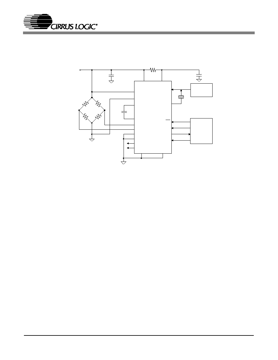
CS5531/32/33/34
42
DS289PP5
OSC2
VD+
VA+
VREF+
VREF-
DGND
VA -
AIN1+
SDI
SCLK
SDO
CS5532
OSC1
CS
10
+5 V
Analog
Supply
0.1 µF
0.1 µF
+
-
17
3
1
2
AIN1-
5
15
9
10
13
11
12
14
16
6
Optional
Clock
Source
Serial
Data
Interface
4.9152 MHz
20
AIN2+
19 AIN2-
7
A0
8
A1
C1
C2
4
22 nF
18
Figure 21. CS5532 Configured with a Single +5 V Supply

CS5531/32/33/34
DS289PP5
43
OSC2
VD+
VA+
VREF+
VREF-
DGND
VA -
AIN1+
SDI
SCLK
SDO
CS5532
OSC1
CS
+2.5 V
Analog
Supply
0.1 µF
0.1 µF
+
-
17
3
1
2
AIN1-
5
15
9
10
13
11
12
14
16
6
Optional
Clock
Source
Serial
Data
Interface
4.9152 MHz
20
AIN2+
19 AIN2-
7
A0
8
A1
C1
C2
4
22 nF
-2.5 V
Analog
Supply
18
+3 V ~ +5 V
Digital
Supply
Figure 22. CS5532 Configured with ±2.5 V Analog Supplies
OSC2
VD+
VA+
VREF+
VREF-
DGND
VA -
AIN1+
SDI
SCLK
SDO
CS5532
OSC1
CS
10
+3 V
Analog
Supply
0.1 µF
0.1 µF
+
-
17
3
1
2
AIN1-
5
15
9
10
13
11
12
14
16
6
Optional
Clock
Source
Serial
Data
Interface
4.9152 MHz
20
AIN2+
19 AIN2-
7
A0
8
A1
C1
C2
4
22 nF
-3 V
Analog
Supply
18
Figure 23. CS5532 Configured with ±3 V Analog Supplies

CS5531/32/33/34
44
DS289PP5
OSC2
VD+
VA+
VREF+
VREF-
DGND
VA -
AIN1+
SDI
SCLK
SDO
CS5532
OSC1
CS
10
+3 V
Analog
Supply
0.1 µF
0.1 µF
17
3
1
2
AIN1-
5
15
9
10
13
11
12
14
16
6
Optional
Clock
Source
Serial
Data
Interface
4.9152 MHz
20
AIN2+
19 AIN2-
7
A0
8
A1
C1
C2
4
22 nF
-3 V
Analog
Supply
18
2.5V
Cold
Junction
Figure 24. CS5532 Configured for Thermocouple Measurement
V+
V+
V
V
V
V
1
2
1
2
(a)
(b)
Figure 25. Bridge with Series Resistors
CS5531/32/33/34
DS289PP5
45
2.12. Getting Started
This A/D converter has several features. From a
software programmer's prospective, what should
be done first? To begin, a 4.9152 MHz or 4.096
MHz crystal takes approximately 20 ms to start. To
accommodate for this, it is recommended that a
software delay of approximately 20 ms start the
processor's ADC initialization code. Next, since
the CS5531/32/33/34 do not provide a power-on-
reset function, the user must first initialize the ADC
to a known state. This is accomplished by resetting
the ADC's serial port with the Serial Port Initializa-
tion sequence. This sequence resets the serial port
to the command mode and is accomplished by
transmitting 15 SYNC1 command bytes (0xFF
hexadecimal), followed by one SYNC0 command
(0xFE hexadecimal). Once the serial port of the
ADC is in the command mode, the user must reset
all the internal logic by performing a system reset
sequence (see 2.3.2 System Reset Sequence). The
next action is to initialize the voltage reference
mode. The voltage reference select (VRS) bit in the
configuration register must be set based upon the
magnitude of the reference voltage between the
VREF+ and the VREF- pins.
After this, the channel-setup registers (CSRs) should
be initialized, as these registers determine how cali-
brations and conversions will be performed. Once
the CSRs are initialized, the user has three options in
calibrating the ADC: 1) don't calibrate and use the
default settings; 2) perform self or system calibra-
tions; or 3) upload previously saved calibration re-
sults to the offset and gain registers. At this point,
the ADC is ready to perform conversions.
2.13. PCB Layout
For optimal performance, the CS5531/32/33/34
should be placed entirely over an analog ground
plane. All grounded pins on the ADC, including the
DGND pin, should be connected to the analog
ground plane that runs beneath the chip. In a split-
plane system, place the analog-digital plane split
immediately adjacent to the digital portion of the
chip.
Note:
See the CDB5531/32/33/34 data sheet for
suggested layout details and Applications
Note 18 for more detailed layout guidelines.
Before layout, please call for our Free
Schematic Review Service.

CS5531/32/33/34
46
DS289PP5
3. PIN DESCRIPTIONS
Clock Generator
OSC1; OSC2 - Master Clock.
An inverting amplifier inside the chip is connected between these pins and can be used with a
crystal to provide the master clock for the device. Alternatively, an external (CMOS
compatible) clock (powered relative to VD+) can be supplied into the OSC2 pin to provide the
master clock for the device.
Control Pins and Serial Data I/O
CS - Chip Select.
When active low, the port will recognize SCLK. When high the SDO pin will output a high
impedance state. CS should be changed when SCLK = 0.
1
2
3
4
5
6
7
8
17
18
19
20
21
22
23
24
9
10
11
12
13
14
15
16
CS5533/4
VREF+
VREF-
CS
DGND
SDO
SERIAL DATA INPUT
POSITIVE ANALOG POWER
AMPLIFIER CAPACITOR CONNECT
AMPLIFIER CAPACITOR CONNECT
DIFFERENTIAL ANALOG INPUT
CHIP SELECT
VOLTAGE REFERENCE INPUT
VOLTAGE REFERENCE INPUT
DIFFERENTIAL ANALOG INPUT
DIFFERENTIAL ANALOG INPUT
POSITIVE DIGITAL POWER
DIGITAL GROUND
SERIAL DATA OUT
MASTER CLOCK
DIFFERENTIAL ANALOG INPUT
AIN3+
AIN3-
SDI
VD+
NEGATIVE ANALOG POWER
DIFFERENTIAL ANALOG INPUT
DIFFERENTIAL ANALOG INPUT
DIFFERENTIAL ANALOG INPUT
DIFFERENTIAL ANALOG INPUT
AIN2-
AIN2+
A1
A0
VA-
VA+
C2
C1
AIN4-
AIN4+
OSC1
OSC2
AIN1-
AIN1+
SCLK
SERIAL CLOCK INPUT
LOGIC OUTPUT (ANALOG)/GUARD
LOGIC OUTPUT (ANALOG)
MASTER CLOCK
1
2
3
4
5
6
7
8
13
14
15
16
17
18
19
20
VREF+
VREF-
SCLK
CS
DGND
A1
A0
VA-
VA+
C2
C1
AIN1-
AIN1+
9
10
11
12
SDO
OSC1
OSC2
SERIAL DATA INPUT
LOGIC OUTPUT (ANALOG)/GUARD
POSITIVE ANALOG POWER
AMPLIFIER CAPACITOR CONNECT
AMPLIFIER CAPACITOR CONNECT
DIFFERENTIAL ANALOG INPUT
CHIP SELECT
VOLTAGE REFERENCE INPUT
VOLTAGE REFERENCE INPUT
DIFFERENTIAL ANALOG INPUT
DIFFERENTIAL ANALOG INPUT
SERIAL CLOCK INPUT
POSITIVE DIGITAL POWER
DIGITAL GROUND
SERIAL DATA OUT
MASTER CLOCK
CS5531/2
DIFFERENTIAL ANALOG INPUT
AIN2+
AIN2-
SDI
VD+
NEGATIVE ANALOG POWER
MASTER CLOCK
LOGIC OUTPUT (ANALOG)

CS5531/32/33/34
DS289PP5
47
SDI - Serial Data Input.
SDI is the input pin of the serial input port. Data will be input at a rate determined by SCLK.
SDO - Serial Data Output.
SDO is the serial data output. It will output a high impedance state if CS = 1.
SCLK - Serial Clock Input.
A clock signal on this pin determines the input/output rate of the data for the SDI/SDO pins
respectively. This input is a Schmitt trigger to allow for slow rise time signals. The SCLK pin
will recognize clocks only when CS is low.
A0 - Logic Output (Analog)/Guard, A1 - Logic Output (Analog).
The logic states of A1-A0 mimic the OL1-OL0 bits in the selected Setup, or the A1-A0 bits in
the Configuration Register, depending on the state of the OLS bit in the Configuration Register.
Logic Output 0 = VA-, and Logic Output 1 = VA+. Alternately, A0 can be used as a guard
drive for the instrumentation amplifier with proper setting of the GB bit in the Configuration
Register.
Measurement and Reference Inputs
AIN1+, AIN1-, AIN2+, AIN2- AIN3+, AIN3-, AIN4+, AIN4- - Differential Analog Input.
Differential input pins into the device.
VREF+, VREF- - Voltage Reference Input.
Fully differential inputs which establish the voltage reference for the on-chip modulator.
C1, C2 - Amplifier Capacitor Inputs.
Connections for the instrumentation amplifier's capacitor.
Power Supply Connections
VA+ - Positive Analog Power.
Positive analog supply voltage.
VD+ - Positive Digital Power.
Positive digital supply voltage (nominally +3.0 V or +5 V).
VA- - Negative Analog Power.
Negative analog supply voltage.
DGND - Digital Ground.
Digital Ground.

CS5531/32/33/34
48
DS289PP5
4. SPECIFICATION DEFINITIONS
Linearity Error
The deviation of a code from a straight line which connects the two endpoints of the ADC
transfer function. One endpoint is located 1/2 LSB below the first code transition and the other
endpoint is located 1/2 LSB beyond the code transition to all ones. Units in percent of full-
scale.
Differential Nonlinearity
The deviation of a code's width from the ideal width. Units in LSBs.
Full Scale Error
The deviation of the last code transition from the ideal [{(VREF+) - (VREF-)} - 3/2 LSB].
Units are in LSBs.
Unipolar Offset
The deviation of the first code transition from the ideal (1/2 LSB above the voltage on the
AIN- pin.). When in unipolar mode (U/B bit = 1). Units are in LSBs.
Bipolar Offset
The deviation of the mid-scale transition (111...111 to 000...000) from the ideal (1/2 LSB below
the voltage on the AIN- pin). When in bipolar mode (U/B bit = 0). Units are in LSBs.
5. ORDERING GUIDE
Model Number
Bits
Channels
Linearity Error (Max)
Temperature Range
Package
CS5531-AS
16
2
±
0.003%
-40
°
C to +85
°
C
20-pin 0.2" Plastic SSOP
CS5533-AS
16
4
±
0.003%
-40
°
C to +85
°
C
24-pin 0.2" Plastic SSOP
CS5532-AS
24
2
±
0.003%
-40
°
C to +85
°
C
20-pin 0.2" Plastic SSOP
CS5532-BS
24
2
±
0.0015%
-40
°
C to +85
°
C
20-pin 0.2" Plastic SSOP
CS5534-AS
24
4
±
0.003%
-40
°
C to +85
°
C
24-pin 0.2" Plastic SSOP
CS5534-BS
24
4
±
0.0015%
-40
°
C to +85
°
C
24-pin 0.2" Plastic SSOP
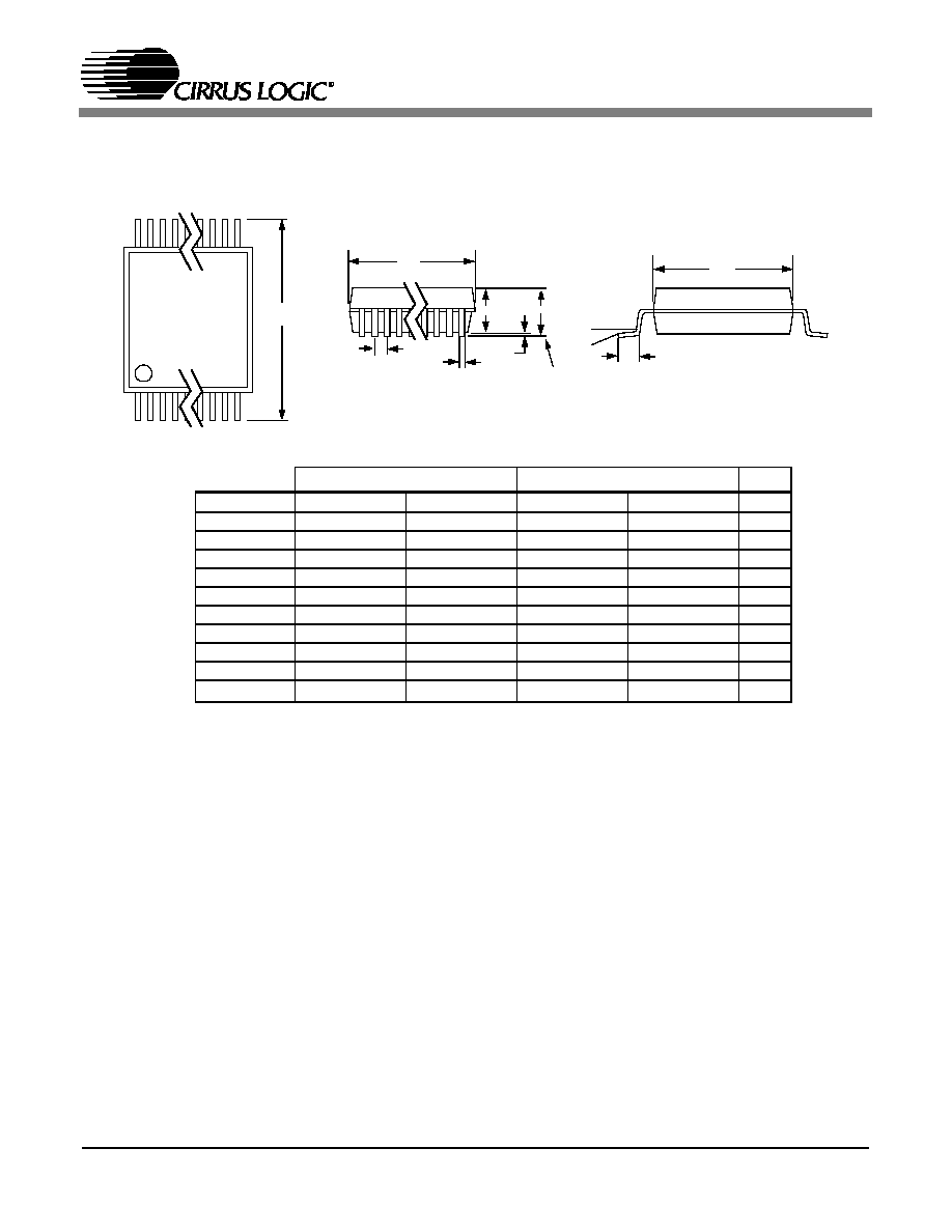
CS5531/32/33/34
DS289PP5
49
6. PACKAGE DRAWINGS
Notes: 1. "D" and "E1" are reference datums and do not included mold flash or protrusions, but do include mold
mismatch and are measured at the parting line, mold flash or protrusions shall not exceed 0.20 mm per
side.
2. Dimension "b" does not include dambar protrusion/intrusion. Allowable dambar protrusion shall be
0.13 mm total in excess of "b" dimension at maximum material condition. Dambar intrusion shall not
reduce dimension "b" by more than 0.07 mm at least material condition.
3. These dimensions apply to the flat section of the lead between 0.10 and 0.25 mm from lead tips.
INCHES
MILLIMETERS
NOTE
DIM
MIN
MAX
MIN
MAX
A
--
0.084
--
2.13
A1
0.002
0.010
0.05
0.25
A2
0.064
0.074
1.62
1.88
b
0.009
0.015
0.22
0.38
2,3
D
0.272
0.295
6.90
7.50
1
E
0.291
0.323
7.40
8.20
E1
0.197
0.220
5.00
5.60
1
e
0.024
0.027
0.61
0.69
L
0.025
0.040
0.63
1.03
0°
8°
0°
8°
20 PIN SSOP PACKAGE DRAWING
E
N
1 2 3
e
b
2
A1
A2
A
D
SEATING
PLANE
E1
1
L
SIDE VIEW
END VIEW
TOP VIEW

CS5531/32/33/34
50
DS289PP5
Notes: 1. "D" and "E1" are reference datums and do not included mold flash or protrusions, but do include mold
mismatch and are measured at the parting line, mold flash or protrusions shall not exceed 0.20 mm per
side.
2. Dimension "b" does not include dambar protrusion/intrusion. Allowable dambar protrusion shall be
0.13 mm total in excess of "b" dimension at maximum material condition. Dambar intrusion shall not
reduce dimension "b" by more than 0.07 mm at least material condition.
3. These dimensions apply to the flat section of the lead between 0.10 and 0.25 mm from lead tips.
INCHES
MILLIMETERS
NOTE
DIM
MIN
MAX
MIN
MAX
A
--
0.084
--
2.13
A1
0.002
0.010
0.05
0.25
A2
0.064
0.074
1.62
1.88
b
0.009
0.015
0.22
0.38
2,3
D
0.311
0.335
7.90
8.50
1
E
0.291
0.323
7.40
8.20
E1
0.197
0.220
5.00
5.60
1
e
0.024
0.027
0.61
0.69
L
0.025
0.040
0.63
1.03
0°
8°
0°
8°
24 PIN SSOP PACKAGE DRAWING
E
N
1 2 3
e
b
2
A1
A2
A
D
SEATING
PLANE
E1
1
L
SIDE VIEW
END VIEW
TOP VIEW

· Notes ·